JP7272969B2 - 固体撮像素子および撮像装置 - Google Patents
固体撮像素子および撮像装置 Download PDFInfo
- Publication number
- JP7272969B2 JP7272969B2 JP2019570639A JP2019570639A JP7272969B2 JP 7272969 B2 JP7272969 B2 JP 7272969B2 JP 2019570639 A JP2019570639 A JP 2019570639A JP 2019570639 A JP2019570639 A JP 2019570639A JP 7272969 B2 JP7272969 B2 JP 7272969B2
- Authority
- JP
- Japan
- Prior art keywords
- pixel
- transistor
- electrode
- potential
- imaging device
- Prior art date
- Legal status (The legal status is an assumption and is not a legal conclusion. Google has not performed a legal analysis and makes no representation as to the accuracy of the status listed.)
- Active
Links
- 238000003384 imaging method Methods 0.000 title claims description 173
- 238000006243 chemical reaction Methods 0.000 claims description 86
- 238000009825 accumulation Methods 0.000 claims description 40
- 239000004065 semiconductor Substances 0.000 claims description 40
- 150000001875 compounds Chemical class 0.000 claims description 9
- 239000002096 quantum dot Substances 0.000 claims description 3
- 239000010408 film Substances 0.000 description 59
- 238000012545 processing Methods 0.000 description 44
- 238000004891 communication Methods 0.000 description 27
- 239000010410 layer Substances 0.000 description 27
- 238000001514 detection method Methods 0.000 description 25
- 238000010586 diagram Methods 0.000 description 25
- 238000012546 transfer Methods 0.000 description 25
- 238000005516 engineering process Methods 0.000 description 23
- 230000006870 function Effects 0.000 description 18
- 238000000034 method Methods 0.000 description 18
- 238000012986 modification Methods 0.000 description 18
- 230000004048 modification Effects 0.000 description 18
- 238000009792 diffusion process Methods 0.000 description 17
- 238000001727 in vivo Methods 0.000 description 15
- 239000002775 capsule Substances 0.000 description 14
- 230000003287 optical effect Effects 0.000 description 14
- 238000002674 endoscopic surgery Methods 0.000 description 12
- 230000003321 amplification Effects 0.000 description 11
- 238000003199 nucleic acid amplification method Methods 0.000 description 11
- 239000000463 material Substances 0.000 description 10
- 230000005540 biological transmission Effects 0.000 description 7
- 230000000694 effects Effects 0.000 description 7
- 239000011229 interlayer Substances 0.000 description 7
- 238000002161 passivation Methods 0.000 description 7
- GPXJNWSHGFTCBW-UHFFFAOYSA-N Indium phosphide Chemical compound [In]#P GPXJNWSHGFTCBW-UHFFFAOYSA-N 0.000 description 6
- 230000008859 change Effects 0.000 description 5
- 239000011810 insulating material Substances 0.000 description 5
- 238000001356 surgical procedure Methods 0.000 description 5
- 229910052581 Si3N4 Inorganic materials 0.000 description 4
- 230000005284 excitation Effects 0.000 description 4
- 230000007246 mechanism Effects 0.000 description 4
- HQVNEWCFYHHQES-UHFFFAOYSA-N silicon nitride Chemical compound N12[Si]34N5[Si]62N3[Si]51N64 HQVNEWCFYHHQES-UHFFFAOYSA-N 0.000 description 4
- 229910000530 Gallium indium arsenide Inorganic materials 0.000 description 3
- 229910000673 Indium arsenide Inorganic materials 0.000 description 3
- PXHVJJICTQNCMI-UHFFFAOYSA-N Nickel Chemical compound [Ni] PXHVJJICTQNCMI-UHFFFAOYSA-N 0.000 description 3
- KDLHZDBZIXYQEI-UHFFFAOYSA-N Palladium Chemical compound [Pd] KDLHZDBZIXYQEI-UHFFFAOYSA-N 0.000 description 3
- 208000005646 Pneumoperitoneum Diseases 0.000 description 3
- 238000011161 development Methods 0.000 description 3
- 238000010336 energy treatment Methods 0.000 description 3
- 239000012535 impurity Substances 0.000 description 3
- RPQDHPTXJYYUPQ-UHFFFAOYSA-N indium arsenide Chemical compound [In]#[As] RPQDHPTXJYYUPQ-UHFFFAOYSA-N 0.000 description 3
- BASFCYQUMIYNBI-UHFFFAOYSA-N platinum Chemical compound [Pt] BASFCYQUMIYNBI-UHFFFAOYSA-N 0.000 description 3
- 239000010936 titanium Substances 0.000 description 3
- 229910018072 Al 2 O 3 Inorganic materials 0.000 description 2
- 229910000661 Mercury cadmium telluride Inorganic materials 0.000 description 2
- 229910004298 SiO 2 Inorganic materials 0.000 description 2
- VYPSYNLAJGMNEJ-UHFFFAOYSA-N Silicium dioxide Chemical compound O=[Si]=O VYPSYNLAJGMNEJ-UHFFFAOYSA-N 0.000 description 2
- RTAQQCXQSZGOHL-UHFFFAOYSA-N Titanium Chemical compound [Ti] RTAQQCXQSZGOHL-UHFFFAOYSA-N 0.000 description 2
- 229910052787 antimony Inorganic materials 0.000 description 2
- WATWJIUSRGPENY-UHFFFAOYSA-N antimony atom Chemical compound [Sb] WATWJIUSRGPENY-UHFFFAOYSA-N 0.000 description 2
- 210000004204 blood vessel Anatomy 0.000 description 2
- 239000003153 chemical reaction reagent Substances 0.000 description 2
- 230000008878 coupling Effects 0.000 description 2
- 238000010168 coupling process Methods 0.000 description 2
- 238000005859 coupling reaction Methods 0.000 description 2
- 239000010931 gold Substances 0.000 description 2
- CJNBYAVZURUTKZ-UHFFFAOYSA-N hafnium(iv) oxide Chemical compound O=[Hf]=O CJNBYAVZURUTKZ-UHFFFAOYSA-N 0.000 description 2
- WPYVAWXEWQSOGY-UHFFFAOYSA-N indium antimonide Chemical compound [Sb]#[In] WPYVAWXEWQSOGY-UHFFFAOYSA-N 0.000 description 2
- MOFVSTNWEDAEEK-UHFFFAOYSA-M indocyanine green Chemical compound [Na+].[O-]S(=O)(=O)CCCCN1C2=CC=C3C=CC=CC3=C2C(C)(C)C1=CC=CC=CC=CC1=[N+](CCCCS([O-])(=O)=O)C2=CC=C(C=CC=C3)C3=C2C1(C)C MOFVSTNWEDAEEK-UHFFFAOYSA-M 0.000 description 2
- 229960004657 indocyanine green Drugs 0.000 description 2
- 238000009434 installation Methods 0.000 description 2
- 230000033001 locomotion Effects 0.000 description 2
- 230000001151 other effect Effects 0.000 description 2
- TWNQGVIAIRXVLR-UHFFFAOYSA-N oxo(oxoalumanyloxy)alumane Chemical compound O=[Al]O[Al]=O TWNQGVIAIRXVLR-UHFFFAOYSA-N 0.000 description 2
- 230000002093 peripheral effect Effects 0.000 description 2
- 238000007639 printing Methods 0.000 description 2
- 229910052814 silicon oxide Inorganic materials 0.000 description 2
- 239000000758 substrate Substances 0.000 description 2
- 230000002194 synthesizing effect Effects 0.000 description 2
- 239000010409 thin film Substances 0.000 description 2
- 229910052719 titanium Inorganic materials 0.000 description 2
- WFKWXMTUELFFGS-UHFFFAOYSA-N tungsten Chemical compound [W] WFKWXMTUELFFGS-UHFFFAOYSA-N 0.000 description 2
- 229910052721 tungsten Inorganic materials 0.000 description 2
- 239000010937 tungsten Substances 0.000 description 2
- 230000000007 visual effect Effects 0.000 description 2
- 239000011701 zinc Substances 0.000 description 2
- JBRZTFJDHDCESZ-UHFFFAOYSA-N AsGa Chemical compound [As]#[Ga] JBRZTFJDHDCESZ-UHFFFAOYSA-N 0.000 description 1
- 229910001218 Gallium arsenide Inorganic materials 0.000 description 1
- 240000004050 Pentaglottis sempervirens Species 0.000 description 1
- 235000004522 Pentaglottis sempervirens Nutrition 0.000 description 1
- 229910010413 TiO 2 Inorganic materials 0.000 description 1
- NRTOMJZYCJJWKI-UHFFFAOYSA-N Titanium nitride Chemical compound [Ti]#N NRTOMJZYCJJWKI-UHFFFAOYSA-N 0.000 description 1
- HCHKCACWOHOZIP-UHFFFAOYSA-N Zinc Chemical compound [Zn] HCHKCACWOHOZIP-UHFFFAOYSA-N 0.000 description 1
- KXNLCSXBJCPWGL-UHFFFAOYSA-N [Ga].[As].[In] Chemical compound [Ga].[As].[In] KXNLCSXBJCPWGL-UHFFFAOYSA-N 0.000 description 1
- 230000001133 acceleration Effects 0.000 description 1
- 229910045601 alloy Inorganic materials 0.000 description 1
- 239000000956 alloy Substances 0.000 description 1
- 229910052782 aluminium Inorganic materials 0.000 description 1
- XAGFODPZIPBFFR-UHFFFAOYSA-N aluminium Chemical compound [Al] XAGFODPZIPBFFR-UHFFFAOYSA-N 0.000 description 1
- 230000000740 bleeding effect Effects 0.000 description 1
- MCMSPRNYOJJPIZ-UHFFFAOYSA-N cadmium;mercury;tellurium Chemical compound [Cd]=[Te]=[Hg] MCMSPRNYOJJPIZ-UHFFFAOYSA-N 0.000 description 1
- 238000002485 combustion reaction Methods 0.000 description 1
- 239000002131 composite material Substances 0.000 description 1
- 239000000470 constituent Substances 0.000 description 1
- 238000010276 construction Methods 0.000 description 1
- 238000012937 correction Methods 0.000 description 1
- 238000013461 design Methods 0.000 description 1
- 238000007599 discharging Methods 0.000 description 1
- 238000007667 floating Methods 0.000 description 1
- 238000002073 fluorescence micrograph Methods 0.000 description 1
- 229910052732 germanium Inorganic materials 0.000 description 1
- GNPVGFCGXDBREM-UHFFFAOYSA-N germanium atom Chemical compound [Ge] GNPVGFCGXDBREM-UHFFFAOYSA-N 0.000 description 1
- PCHJSUWPFVWCPO-UHFFFAOYSA-N gold Chemical compound [Au] PCHJSUWPFVWCPO-UHFFFAOYSA-N 0.000 description 1
- 229910052737 gold Inorganic materials 0.000 description 1
- 230000006872 improvement Effects 0.000 description 1
- AMGQUBHHOARCQH-UHFFFAOYSA-N indium;oxotin Chemical compound [In].[Sn]=O AMGQUBHHOARCQH-UHFFFAOYSA-N 0.000 description 1
- 210000000936 intestine Anatomy 0.000 description 1
- 230000001678 irradiating effect Effects 0.000 description 1
- 230000031700 light absorption Effects 0.000 description 1
- 238000012423 maintenance Methods 0.000 description 1
- 238000005259 measurement Methods 0.000 description 1
- 229910044991 metal oxide Inorganic materials 0.000 description 1
- 150000004706 metal oxides Chemical class 0.000 description 1
- 238000002406 microsurgery Methods 0.000 description 1
- 239000003595 mist Substances 0.000 description 1
- 230000000116 mitigating effect Effects 0.000 description 1
- 229910052759 nickel Inorganic materials 0.000 description 1
- 239000013307 optical fiber Substances 0.000 description 1
- 210000000056 organ Anatomy 0.000 description 1
- 229910052763 palladium Inorganic materials 0.000 description 1
- 230000002572 peristaltic effect Effects 0.000 description 1
- 229910052697 platinum Inorganic materials 0.000 description 1
- 238000011084 recovery Methods 0.000 description 1
- 230000009467 reduction Effects 0.000 description 1
- 230000004044 response Effects 0.000 description 1
- 238000007789 sealing Methods 0.000 description 1
- 230000035945 sensitivity Effects 0.000 description 1
- 230000035939 shock Effects 0.000 description 1
- 210000002784 stomach Anatomy 0.000 description 1
- 239000002344 surface layer Substances 0.000 description 1
- JBQYATWDVHIOAR-UHFFFAOYSA-N tellanylidenegermanium Chemical compound [Te]=[Ge] JBQYATWDVHIOAR-UHFFFAOYSA-N 0.000 description 1
- 229910052725 zinc Inorganic materials 0.000 description 1
Images


Classifications
-
- H—ELECTRICITY
- H04—ELECTRIC COMMUNICATION TECHNIQUE
- H04N—PICTORIAL COMMUNICATION, e.g. TELEVISION
- H04N25/00—Circuitry of solid-state image sensors [SSIS]; Control thereof
- H04N25/50—Control of the SSIS exposure
- H04N25/57—Control of the dynamic range
- H04N25/59—Control of the dynamic range by controlling the amount of charge storable in the pixel, e.g. modification of the charge conversion ratio of the floating node capacitance
-
- H—ELECTRICITY
- H01—ELECTRIC ELEMENTS
- H01L—SEMICONDUCTOR DEVICES NOT COVERED BY CLASS H10
- H01L27/00—Devices consisting of a plurality of semiconductor or other solid-state components formed in or on a common substrate
- H01L27/14—Devices consisting of a plurality of semiconductor or other solid-state components formed in or on a common substrate including semiconductor components sensitive to infrared radiation, light, electromagnetic radiation of shorter wavelength or corpuscular radiation and specially adapted either for the conversion of the energy of such radiation into electrical energy or for the control of electrical energy by such radiation
- H01L27/144—Devices controlled by radiation
- H01L27/146—Imager structures
- H01L27/14601—Structural or functional details thereof
- H01L27/14603—Special geometry or disposition of pixel-elements, address-lines or gate-electrodes
- H01L27/14605—Structural or functional details relating to the position of the pixel elements, e.g. smaller pixel elements in the center of the imager compared to pixel elements at the periphery
-
- H—ELECTRICITY
- H01—ELECTRIC ELEMENTS
- H01L—SEMICONDUCTOR DEVICES NOT COVERED BY CLASS H10
- H01L27/00—Devices consisting of a plurality of semiconductor or other solid-state components formed in or on a common substrate
- H01L27/14—Devices consisting of a plurality of semiconductor or other solid-state components formed in or on a common substrate including semiconductor components sensitive to infrared radiation, light, electromagnetic radiation of shorter wavelength or corpuscular radiation and specially adapted either for the conversion of the energy of such radiation into electrical energy or for the control of electrical energy by such radiation
- H01L27/144—Devices controlled by radiation
- H01L27/146—Imager structures
- H01L27/14601—Structural or functional details thereof
- H01L27/14603—Special geometry or disposition of pixel-elements, address-lines or gate-electrodes
- H01L27/14607—Geometry of the photosensitive area
-
- H—ELECTRICITY
- H01—ELECTRIC ELEMENTS
- H01L—SEMICONDUCTOR DEVICES NOT COVERED BY CLASS H10
- H01L27/00—Devices consisting of a plurality of semiconductor or other solid-state components formed in or on a common substrate
- H01L27/14—Devices consisting of a plurality of semiconductor or other solid-state components formed in or on a common substrate including semiconductor components sensitive to infrared radiation, light, electromagnetic radiation of shorter wavelength or corpuscular radiation and specially adapted either for the conversion of the energy of such radiation into electrical energy or for the control of electrical energy by such radiation
- H01L27/144—Devices controlled by radiation
- H01L27/146—Imager structures
- H01L27/14601—Structural or functional details thereof
- H01L27/14609—Pixel-elements with integrated switching, control, storage or amplification elements
- H01L27/14612—Pixel-elements with integrated switching, control, storage or amplification elements involving a transistor
-
- H—ELECTRICITY
- H01—ELECTRIC ELEMENTS
- H01L—SEMICONDUCTOR DEVICES NOT COVERED BY CLASS H10
- H01L27/00—Devices consisting of a plurality of semiconductor or other solid-state components formed in or on a common substrate
- H01L27/14—Devices consisting of a plurality of semiconductor or other solid-state components formed in or on a common substrate including semiconductor components sensitive to infrared radiation, light, electromagnetic radiation of shorter wavelength or corpuscular radiation and specially adapted either for the conversion of the energy of such radiation into electrical energy or for the control of electrical energy by such radiation
- H01L27/144—Devices controlled by radiation
- H01L27/146—Imager structures
- H01L27/14601—Structural or functional details thereof
- H01L27/14625—Optical elements or arrangements associated with the device
-
- H—ELECTRICITY
- H01—ELECTRIC ELEMENTS
- H01L—SEMICONDUCTOR DEVICES NOT COVERED BY CLASS H10
- H01L27/00—Devices consisting of a plurality of semiconductor or other solid-state components formed in or on a common substrate
- H01L27/14—Devices consisting of a plurality of semiconductor or other solid-state components formed in or on a common substrate including semiconductor components sensitive to infrared radiation, light, electromagnetic radiation of shorter wavelength or corpuscular radiation and specially adapted either for the conversion of the energy of such radiation into electrical energy or for the control of electrical energy by such radiation
- H01L27/144—Devices controlled by radiation
- H01L27/146—Imager structures
- H01L27/14601—Structural or functional details thereof
- H01L27/14636—Interconnect structures
-
- H—ELECTRICITY
- H01—ELECTRIC ELEMENTS
- H01L—SEMICONDUCTOR DEVICES NOT COVERED BY CLASS H10
- H01L27/00—Devices consisting of a plurality of semiconductor or other solid-state components formed in or on a common substrate
- H01L27/14—Devices consisting of a plurality of semiconductor or other solid-state components formed in or on a common substrate including semiconductor components sensitive to infrared radiation, light, electromagnetic radiation of shorter wavelength or corpuscular radiation and specially adapted either for the conversion of the energy of such radiation into electrical energy or for the control of electrical energy by such radiation
- H01L27/144—Devices controlled by radiation
- H01L27/146—Imager structures
- H01L27/14601—Structural or functional details thereof
- H01L27/14641—Electronic components shared by two or more pixel-elements, e.g. one amplifier shared by two pixel elements
-
- H—ELECTRICITY
- H01—ELECTRIC ELEMENTS
- H01L—SEMICONDUCTOR DEVICES NOT COVERED BY CLASS H10
- H01L27/00—Devices consisting of a plurality of semiconductor or other solid-state components formed in or on a common substrate
- H01L27/14—Devices consisting of a plurality of semiconductor or other solid-state components formed in or on a common substrate including semiconductor components sensitive to infrared radiation, light, electromagnetic radiation of shorter wavelength or corpuscular radiation and specially adapted either for the conversion of the energy of such radiation into electrical energy or for the control of electrical energy by such radiation
- H01L27/144—Devices controlled by radiation
- H01L27/146—Imager structures
- H01L27/14643—Photodiode arrays; MOS imagers
- H01L27/14649—Infrared imagers
- H01L27/14652—Multispectral infrared imagers, having a stacked pixel-element structure, e.g. npn, npnpn or MQW structures
-
- H—ELECTRICITY
- H04—ELECTRIC COMMUNICATION TECHNIQUE
- H04N—PICTORIAL COMMUNICATION, e.g. TELEVISION
- H04N25/00—Circuitry of solid-state image sensors [SSIS]; Control thereof
- H04N25/20—Circuitry of solid-state image sensors [SSIS]; Control thereof for transforming only infrared radiation into image signals
-
- H—ELECTRICITY
- H04—ELECTRIC COMMUNICATION TECHNIQUE
- H04N—PICTORIAL COMMUNICATION, e.g. TELEVISION
- H04N25/00—Circuitry of solid-state image sensors [SSIS]; Control thereof
- H04N25/40—Extracting pixel data from image sensors by controlling scanning circuits, e.g. by modifying the number of pixels sampled or to be sampled
- H04N25/46—Extracting pixel data from image sensors by controlling scanning circuits, e.g. by modifying the number of pixels sampled or to be sampled by combining or binning pixels
-
- H—ELECTRICITY
- H04—ELECTRIC COMMUNICATION TECHNIQUE
- H04N—PICTORIAL COMMUNICATION, e.g. TELEVISION
- H04N25/00—Circuitry of solid-state image sensors [SSIS]; Control thereof
- H04N25/50—Control of the SSIS exposure
- H04N25/53—Control of the integration time
-
- H—ELECTRICITY
- H04—ELECTRIC COMMUNICATION TECHNIQUE
- H04N—PICTORIAL COMMUNICATION, e.g. TELEVISION
- H04N25/00—Circuitry of solid-state image sensors [SSIS]; Control thereof
- H04N25/70—SSIS architectures; Circuits associated therewith
- H04N25/71—Charge-coupled device [CCD] sensors; Charge-transfer registers specially adapted for CCD sensors
- H04N25/75—Circuitry for providing, modifying or processing image signals from the pixel array
-
- H—ELECTRICITY
- H04—ELECTRIC COMMUNICATION TECHNIQUE
- H04N—PICTORIAL COMMUNICATION, e.g. TELEVISION
- H04N25/00—Circuitry of solid-state image sensors [SSIS]; Control thereof
- H04N25/70—SSIS architectures; Circuits associated therewith
- H04N25/76—Addressed sensors, e.g. MOS or CMOS sensors
-
- H—ELECTRICITY
- H04—ELECTRIC COMMUNICATION TECHNIQUE
- H04N—PICTORIAL COMMUNICATION, e.g. TELEVISION
- H04N25/00—Circuitry of solid-state image sensors [SSIS]; Control thereof
- H04N25/70—SSIS architectures; Circuits associated therewith
- H04N25/76—Addressed sensors, e.g. MOS or CMOS sensors
- H04N25/766—Addressed sensors, e.g. MOS or CMOS sensors comprising control or output lines used for a plurality of functions, e.g. for pixel output, driving, reset or power
-
- H—ELECTRICITY
- H04—ELECTRIC COMMUNICATION TECHNIQUE
- H04N—PICTORIAL COMMUNICATION, e.g. TELEVISION
- H04N25/00—Circuitry of solid-state image sensors [SSIS]; Control thereof
- H04N25/70—SSIS architectures; Circuits associated therewith
- H04N25/79—Arrangements of circuitry being divided between different or multiple substrates, chips or circuit boards, e.g. stacked image sensors
-
- H—ELECTRICITY
- H04—ELECTRIC COMMUNICATION TECHNIQUE
- H04N—PICTORIAL COMMUNICATION, e.g. TELEVISION
- H04N5/00—Details of television systems
- H04N5/30—Transforming light or analogous information into electric information
- H04N5/33—Transforming infrared radiation
Landscapes
- Engineering & Computer Science (AREA)
- Physics & Mathematics (AREA)
- Power Engineering (AREA)
- Computer Hardware Design (AREA)
- General Physics & Mathematics (AREA)
- Condensed Matter Physics & Semiconductors (AREA)
- Electromagnetism (AREA)
- Microelectronics & Electronic Packaging (AREA)
- Multimedia (AREA)
- Signal Processing (AREA)
- Spectroscopy & Molecular Physics (AREA)
- Solid State Image Pick-Up Elements (AREA)
- Transforming Light Signals Into Electric Signals (AREA)
Description
1.第1の実施の形態(リセットトランジスタに直列に接続された電位生成部を有する固体撮像素子の例)
2.第2の実施の形態(リセットトランジスタに並列に接続された電位生成部を有する固体撮像素子の例)
3.変形例1(容量切替用のトランジスタを有する例)
4.変形例2(グローバルシャッター機能を有する例)
5.第3の実施の形態(第1電荷蓄積部(FD)に直列に接続された電位生成部を有する固体撮像素子の例)
6.第4の実施の形態(転送トランジスタおよび第2電荷蓄積部を含む電位生成部を有する固体撮像素子の例)
7.変形例3(読出画素および非読出画素の配置例)
8.適用例(電子機器の例)
9.応用例
[撮像素子1の構成]
図1は、本開示の一実施の形態に係る固体撮像素子(撮像素子1)の機能構成の一例を模式的に表したものである。撮像素子1は、例えば赤外線イメージセンサであり、例えば波長800nm以上の光に対しても感度を有している。この撮像素子1には、例えば四角形状の画素領域10Pと、画素領域10Pの外側の画素外領域10Bとが設けられている。画素外領域10Bには、画素領域10Pを駆動するための周辺回路が設けられている。
図5を用いて撮像素子1の動作について説明する。撮像素子1では、第2電極15および第2半導体層14を介して、光電変換膜13へ光(例えば赤外領域の波長の光)が入射すると、この光は光電変換膜13において吸収される。これにより、各画素Pの光電変換膜13では正孔(ホール)および電子の対が発生する(光電変換される)。このとき、読出画素Prでは、例えば第1電極11に所定の電位(例えばリセット電位VRST)が印加されると、第1電極11と第2電極15との間に電位勾配が生じ、発生した電荷のうち一方の電荷(例えば正孔)が、信号電荷として拡散領域12Aに移動し、拡散領域12Aから画素P毎に第1電極11へ収集される。
本実施の形態の撮像素子1では、非読出画素Pnの画素回路20Pnに、電位生成部23が設けられているので、蓄積期間T10では、非読出画素Pnの第1電極11に、電位生成部23で生成された電位VPDが印加される。これにより、非読出画素Pnでは、第1電極11と第2電極15との間の電位差が小さくなり、この非読出画素Pnで発生した信号電荷は、近傍の読出画素Prの拡散領域12Aに移動する。したがって、読出画素Prの画素回路20Prからは、読出画素Prで発生した信号電荷と、非読出画素Pnで発生した信号電荷とが合算されて読み出される。
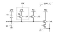
図7A,図7Bは、第2の実施の形態に係る撮像素子(撮像素子1A)の画素回路20Pr,20Pnの回路構成を表したものである。この画素回路20Pr,20Pnは、光電変換部10(第1電極11)とリセットトランジスタ22との間に、リセットトランジスタ22に並列に接続された電位生成部(電位生成部23A)を有している。この点を除き、第2の実施の形態に係る撮像素子1Aは、上記第1の実施の形態の撮像素子1と同様の構成を有し、その作用および効果も同様である。
上記第2の実施の形態では、読出画素Prの画素回路20Prと、非読出画素Pnの画素回路20Pnとが同じ構成を有している例について説明したが、これらは互いに異なる構成を有していてもよい。
図10は、上記第2の実施の形態の変形例(変形例2)に係る画素回路20Pr,20Pnの回路構成の一例を表している。この画素回路20Pr,20Pnは、光電変換部10に接続された電荷蓄積部31と、電荷蓄積部31とFD21との間に配置された転送トランジスタ32とを含むものである。このように、画素回路20Pr,20Pnに電荷蓄積部31および転送トランジスタ32を設けることにより、グローバルシャッター機能を有する撮像素子1Aを実現可能となる。
図11A,図11Bは、第3の実施の形態に係る撮像素子(撮像素子1B)の画素回路20Pr,20Pnの回路構成を表したものである。この画素回路20Pr,20Pnは、光電変換部10(第1電極11)とFD21との間に、光電変換部10に直列に接続された電位生成部(電位生成部23B)を有している。この点を除き、第3の実施の形態に係る撮像素子1Bは、上記第1の実施の形態の撮像素子1と同様の構成を有し、その作用および効果も同様である。
図14A,図14Bは、第4の実施の形態に係る撮像素子(撮像素子1C)の画素回路20Pr,20Pnの回路構成を表したものである。撮像素子1Cはグローバルシャッター機能を有する撮像素子であり、画素回路20Pr,20Pnの電位生成部(電位生成部23C)は、画素P毎に設けられた電荷蓄積部31(第2電荷蓄積部)と、電荷蓄積部31とFD21との間に設けられた転送トランジスタ32(第2トランジスタ)とを含んでいる。この点を除き、第4の実施の形態に係る撮像素子1Cは、上記第1の実施の形態の撮像素子1と同様の構成を有し、その作用および効果も同様である。
上述の図2では、読出画素Prおよび非読出画素Pnを画素P行毎に、交互に配置する例を示したが、読出画素Prおよび非読出画素Pnは自由に配置することが可能である。例えば、図示は省略するが、読出画素Prおよび非読出画素Pnを画素Pの列毎に、交互に配置するようにしてもよい。
上述の撮像素子1,1A,1B,1Cは、例えば赤外領域を撮像可能なカメラなど、様々なタイプの撮像装置(電子機器)に適用することができる。図22に、その一例として、電子機器3(カメラ)の概略構成を示す。この電子機器3は、例えば静止画または動画を撮影可能なカメラであり、撮像素子1,1A,1B,1Cと、光学系(光学レンズ)310と、シャッタ装置311と、撮像素子1,1A,1B,1Cおよびシャッタ装置311を駆動する駆動部313と、信号処理部312とを有する。
更に、本開示に係る技術(本技術)は、様々な製品へ応用することができる。例えば、本開示に係る技術は、内視鏡手術システムに適用されてもよい。
本開示に係る技術(本技術)は、様々な製品へ応用することができる。例えば、本開示に係る技術は、内視鏡手術システムに適用されてもよい。
本開示に係る技術は、様々な製品へ応用することができる。例えば、本開示に係る技術は、自動車、電気自動車、ハイブリッド電気自動車、自動二輪車、自転車、パーソナルモビリティ、飛行機、ドローン、船舶、ロボット、建設機械、農業機械(トラクター)などのいずれかの種類の移動体に搭載される装置として実現されてもよい。
(1)
複数の画素にわたって設けられた光電変換膜と、
前記光電変換膜に電気的に接続され、画素毎に設けられた第1電極と、
前記光電変換膜を間にして前記第1電極に対向する第2電極と、
前記光電変換膜で生成され、前記第1電極を介して移動した信号電荷を蓄積する第1電荷蓄積部と、
画素毎に設けられ、前記第1電荷蓄積部にリセット電位を印加するリセットトランジスタと、
前記第1電荷蓄積部に前記信号電荷が蓄積される期間、前記複数の画素の少なくとも一部の画素の前記第1電極に、前記リセット電位よりも前記第2電極との間の電位差を小さくする電位VPDを印加する電位生成部と
を備えた固体撮像素子。
(2)
前記電位生成部は、前記リセットトランジスタを介して前記第1電極に接続されている
前記(1)に記載の固体撮像素子。
(3)
前記電位生成部は、第1トランジスタを含む
前記(1)に記載の固体撮像素子。
(4)
前記第1トランジスタは、前記電位VPDに接続され、前記第1電極と前記リセットトランジスタとの間に、前記リセットトランジスタに並列に接続されている
前記(3)に記載の固体撮像素子。
(5)
前記第1トランジスタが、前記期間にオン状態になるように構成された
前記(4)に記載の固体撮像素子。
(6)
前記第1トランジスタは、前記第1電極と前記第1電荷蓄積部との間に、前記第1電荷蓄積部に直列に接続されている
前記(3)に記載の固体撮像素子。
(7)
前記第1トランジスタが、前記期間にオフ状態になるように構成された
前記(6)に記載の固体撮像素子。
(8)
前記電位生成部は、前記第1電極と前記第1電荷蓄積部との間に、画素毎に設けられた第2電荷蓄積部と、前記第2電荷蓄積部と前記第1電荷蓄積部との間に設けられた第2トランジスタとを含む
前記(1)に記載の固体撮像素子。
(9)
前記第2トランジスタが、前記期間にオフ状態になるように構成された
前記(8)に記載の固体撮像素子。
(10)
更に、前記第1電極に前記電位VPDが印加される前記画素を選択する制御線を含む
前記(1)ないし(9)のうちいずれか1つに記載の固体撮像素子。
(11)
前記複数の画素は、第1方向および前記第1方向に交差する第2方向に沿って配置され、
前記制御線は、前記第1方向および前記第2方向の少なくとも一方に沿って設けられている
前記(10)に記載の固体撮像素子。
(12)
更に、前記第1電極に前記電位VPDが印加される画素以外の画素の前記第1電荷蓄積部に接続された、容量切替用の第3トランジスタと、
前記第3トランジスタに接続された付加容量素子とを含む
前記(1)に記載の固体撮像素子。
(13)
前記光電変換膜は化合物半導体、有機半導体または量子ドットを含む
前記(1)ないし(12)のうちいずれか1つに記載の固体撮像素子。
(14)
前記第1電極に前記電位VPDが印加される画素の前記光電変換膜で生成された信号電荷は、それ以外の画素の前記第1電荷蓄積部に移動する
前記(1)ないし(13)のうちいずれか1つに記載の固体撮像素子。
(15)
複数の画素にわたって設けられた光電変換膜と、
前記光電変換膜に電気的に接続され、画素毎に設けられた第1電極と、
前記光電変換膜を間にして前記第1電極に対向する第2電極と、
前記光電変換膜で生成され、前記第1電極を介して移動した信号電荷を蓄積する第1電荷蓄積部と、
画素毎に設けられ、前記第1電荷蓄積部にリセット電位を印加するリセットトランジスタと、
前記第1電荷蓄積部に前記信号電荷が蓄積される期間、前記複数の画素の少なくとも一部の画素の前記第1電極に、前記リセット電位よりも前記第2電極との間の電位差を小さくする電位VPDを印加する電位生成部とを備えた
固体撮像素子を有する撮像装置。
Claims (15)
- 複数の画素にわたって設けられた光電変換膜と、
前記光電変換膜に電気的に接続され、画素毎に設けられた第1電極と、
前記光電変換膜を間にして前記第1電極に対向する第2電極と、
前記光電変換膜で生成され、前記第1電極を介して移動した信号電荷を蓄積する第1電荷蓄積部と、
画素毎に設けられ、前記第1電荷蓄積部にリセット電位を印加するリセットトランジスタと、
前記第1電荷蓄積部に前記信号電荷が蓄積される期間、前記複数の画素の少なくとも一部の画素の前記第1電極に、前記リセット電位よりも前記第2電極との間の電位差を小さくする電位VPDを印加する電位生成部と
を備えた固体撮像素子。 - 前記電位生成部は、前記リセットトランジスタを介して前記第1電極に接続されている
請求項1に記載の固体撮像素子。 - 前記電位生成部は、第1トランジスタを含む
請求項1に記載の固体撮像素子。 - 前記第1トランジスタは、前記電位VPDに接続され、前記第1電極と前記リセットトランジスタとの間に、前記リセットトランジスタに並列に接続されている
請求項3に記載の固体撮像素子。 - 前記第1トランジスタが、前記期間にオン状態になるように構成された
請求項4に記載の固体撮像素子。 - 前記第1トランジスタは、前記第1電極と前記第1電荷蓄積部との間に、前記第1電荷蓄積部に直列に接続されている
請求項3に記載の固体撮像素子。 - 前記第1トランジスタが、前記期間にオフ状態になるように構成された
請求項6に記載の固体撮像素子。 - 前記電位生成部は、前記第1電極と前記第1電荷蓄積部との間に、画素毎に設けられた第2電荷蓄積部と、前記第2電荷蓄積部と前記第1電荷蓄積部との間に設けられた第2トランジスタとを含む
請求項1に記載の固体撮像素子。 - 前記第2トランジスタが、前記期間にオフ状態になるように構成された
請求項8に記載の固体撮像素子。 - 更に、前記第1電極に前記電位VPDが印加される前記画素を選択する制御線を含む
請求項1に記載の固体撮像素子。 - 前記複数の画素は、第1方向および前記第1方向に交差する第2方向に沿って配置され、
前記制御線は、前記第1方向および前記第2方向の少なくとも一方に沿って設けられている
請求項10に記載の固体撮像素子。 - 更に、前記第1電極に前記電位VPDが印加される画素以外の画素の前記第1電荷蓄積部に接続された、容量切替用の第3トランジスタと、
前記第3トランジスタに接続された付加容量素子とを含む
請求項1に記載の固体撮像素子。 - 前記光電変換膜は化合物半導体、有機半導体または量子ドットを含む
請求項1に記載の固体撮像素子。 - 前記第1電極に前記電位VPDが印加される画素の前記光電変換膜で生成された信号電荷は、それ以外の画素の前記第1電荷蓄積部に移動する
請求項1に記載の固体撮像素子。 - 複数の画素にわたって設けられた光電変換膜と、
前記光電変換膜に電気的に接続され、画素毎に設けられた第1電極と、
前記光電変換膜を間にして前記第1電極に対向する第2電極と、
前記光電変換膜で生成され、前記第1電極を介して移動した信号電荷を蓄積する第1電荷蓄積部と、
画素毎に設けられ、前記第1電荷蓄積部にリセット電位を印加するリセットトランジスタと、
前記第1電荷蓄積部に前記信号電荷が蓄積される期間、前記複数の画素の少なくとも一部の画素の前記第1電極に、前記リセット電位よりも前記第2電極との間の電位差を小さくする電位VPDを印加する電位生成部とを備えた
固体撮像素子を有する撮像装置。
Priority Applications (1)
| Application Number | Priority Date | Filing Date | Title |
|---|---|---|---|
| JP2023071982A JP2023100745A (ja) | 2018-02-07 | 2023-04-26 | 固体撮像素子および撮像装置 |
Applications Claiming Priority (5)
| Application Number | Priority Date | Filing Date | Title |
|---|---|---|---|
| JP2018020098 | 2018-02-07 | ||
| JP2018020098 | 2018-02-07 | ||
| JP2018034466 | 2018-02-28 | ||
| JP2018034466 | 2018-02-28 | ||
| PCT/JP2019/001236 WO2019155841A1 (ja) | 2018-02-07 | 2019-01-17 | 固体撮像素子および撮像装置 |
Related Child Applications (1)
| Application Number | Title | Priority Date | Filing Date |
|---|---|---|---|
| JP2023071982A Division JP2023100745A (ja) | 2018-02-07 | 2023-04-26 | 固体撮像素子および撮像装置 |
Publications (3)
| Publication Number | Publication Date |
|---|---|
| JPWO2019155841A1 JPWO2019155841A1 (ja) | 2021-02-04 |
| JPWO2019155841A5 JPWO2019155841A5 (ja) | 2022-01-17 |
| JP7272969B2 true JP7272969B2 (ja) | 2023-05-12 |
Family
ID=67549599
Family Applications (2)
| Application Number | Title | Priority Date | Filing Date |
|---|---|---|---|
| JP2019570639A Active JP7272969B2 (ja) | 2018-02-07 | 2019-01-17 | 固体撮像素子および撮像装置 |
| JP2023071982A Pending JP2023100745A (ja) | 2018-02-07 | 2023-04-26 | 固体撮像素子および撮像装置 |
Family Applications After (1)
| Application Number | Title | Priority Date | Filing Date |
|---|---|---|---|
| JP2023071982A Pending JP2023100745A (ja) | 2018-02-07 | 2023-04-26 | 固体撮像素子および撮像装置 |
Country Status (6)
| Country | Link |
|---|---|
| US (2) | US11595596B2 (ja) |
| EP (1) | EP3751840B1 (ja) |
| JP (2) | JP7272969B2 (ja) |
| KR (1) | KR102609647B1 (ja) |
| CN (2) | CN111656769B (ja) |
| WO (1) | WO2019155841A1 (ja) |
Families Citing this family (7)
| Publication number | Priority date | Publication date | Assignee | Title |
|---|---|---|---|---|
| WO2019155841A1 (ja) | 2018-02-07 | 2019-08-15 | ソニーセミコンダクタソリューションズ株式会社 | 固体撮像素子および撮像装置 |
| US11769782B2 (en) * | 2018-05-02 | 2023-09-26 | Sony Semiconductor Solutions Corporation | Solid-state imaging element and imaging apparatus |
| JP7486929B2 (ja) * | 2019-08-22 | 2024-05-20 | ソニーセミコンダクタソリューションズ株式会社 | 撮像素子、測距装置 |
| JP7414569B2 (ja) | 2020-02-12 | 2024-01-16 | ソニーセミコンダクタソリューションズ株式会社 | 固体撮像素子 |
| US20230187469A1 (en) * | 2020-05-26 | 2023-06-15 | Sony Semiconductor Solutions Corporation | Solid-state imaging element |
| US20240163585A1 (en) * | 2021-03-22 | 2024-05-16 | Sony Semiconductor Solutions Corporation | Imaging device |
| JPWO2022208949A1 (ja) * | 2021-03-31 | 2022-10-06 |
Citations (3)
| Publication number | Priority date | Publication date | Assignee | Title |
|---|---|---|---|---|
| JP2014216978A (ja) | 2013-04-30 | 2014-11-17 | 富士フイルム株式会社 | 固体撮像素子および撮像装置 |
| JP2016086407A (ja) | 2014-10-23 | 2016-05-19 | パナソニックIpマネジメント株式会社 | 撮像装置および画像取得装置 |
| WO2017150167A1 (ja) | 2016-02-29 | 2017-09-08 | ソニー株式会社 | 固体撮像素子 |
Family Cites Families (19)
| Publication number | Priority date | Publication date | Assignee | Title |
|---|---|---|---|---|
| JP5124369B2 (ja) * | 2008-07-03 | 2013-01-23 | 富士フイルム株式会社 | 撮像装置及び固体撮像素子の駆動方法 |
| US20120211642A1 (en) * | 2009-10-27 | 2012-08-23 | Konica Minolta Opto, Inc. | Solid-State Imaging Device |
| JPWO2012164829A1 (ja) * | 2011-05-31 | 2015-02-23 | パナソニック株式会社 | 撮像装置 |
| JP5935293B2 (ja) * | 2011-11-02 | 2016-06-15 | ソニー株式会社 | 撮像装置および撮像表示システム |
| JP6233718B2 (ja) * | 2012-12-27 | 2017-11-22 | パナソニックIpマネジメント株式会社 | 撮像装置及びその駆動方法 |
| JP6171997B2 (ja) * | 2014-03-14 | 2017-08-02 | ソニー株式会社 | 固体撮像素子およびその駆動方法、並びに電子機器 |
| JP6385187B2 (ja) * | 2014-07-31 | 2018-09-05 | キヤノン株式会社 | 光電変換装置、光電変換システム |
| DE102014220921A1 (de) * | 2014-10-15 | 2016-04-21 | Henkel Ag & Co. Kgaa | Verfahren zum gleichzeitigen permanenten Umformen und Färben keratinischer Fasern I |
| US10141354B2 (en) | 2014-10-23 | 2018-11-27 | Panasonic Intellectual Property Management Co., Ltd. | Imaging device and image acquisition device |
| US10212372B2 (en) * | 2014-12-26 | 2019-02-19 | Panasonic Intellectual Property Management Co., Ltd. | Imaging device including signal line and unit pixel cell including charge storage region |
| KR101773103B1 (ko) | 2015-01-09 | 2017-08-30 | 주식회사 엘지화학 | 전극, 이의 제조방법, 이에 의해 제조된 전극 및 이를 포함하는 이차전지 |
| CN107018289B (zh) * | 2016-01-22 | 2021-01-19 | 松下知识产权经营株式会社 | 摄像装置 |
| US10313609B2 (en) * | 2016-04-14 | 2019-06-04 | Qualcomm Incorporated | Image sensors having pixel-binning with configurable shared floating diffusion |
| EP3284410B1 (en) | 2016-06-13 | 2020-06-03 | Shanghai United Imaging Healthcare Co., Ltd. | Systems for x-ray scanner positioning |
| JP2018034466A (ja) | 2016-09-01 | 2018-03-08 | 独立行政法人 国立印刷局 | 潜像凹版模様を有する印刷物 |
| JP6920652B2 (ja) * | 2017-02-03 | 2021-08-18 | パナソニックIpマネジメント株式会社 | 撮像装置 |
| CN110945865B (zh) * | 2017-12-28 | 2023-06-13 | 松下知识产权经营株式会社 | 摄像装置 |
| WO2019155841A1 (ja) | 2018-02-07 | 2019-08-15 | ソニーセミコンダクタソリューションズ株式会社 | 固体撮像素子および撮像装置 |
| WO2020217783A1 (ja) * | 2019-04-25 | 2020-10-29 | パナソニックIpマネジメント株式会社 | 撮像装置 |
-
2019
- 2019-01-17 WO PCT/JP2019/001236 patent/WO2019155841A1/ja unknown
- 2019-01-17 KR KR1020207018290A patent/KR102609647B1/ko active IP Right Grant
- 2019-01-17 EP EP19750263.6A patent/EP3751840B1/en active Active
- 2019-01-17 JP JP2019570639A patent/JP7272969B2/ja active Active
- 2019-01-17 CN CN201980010831.8A patent/CN111656769B/zh active Active
- 2019-01-17 US US16/966,130 patent/US11595596B2/en active Active
- 2019-01-17 CN CN202310531452.1A patent/CN116744130A/zh active Pending
-
2023
- 2023-01-12 US US18/096,518 patent/US11895415B2/en active Active
- 2023-04-26 JP JP2023071982A patent/JP2023100745A/ja active Pending
Patent Citations (3)
| Publication number | Priority date | Publication date | Assignee | Title |
|---|---|---|---|---|
| JP2014216978A (ja) | 2013-04-30 | 2014-11-17 | 富士フイルム株式会社 | 固体撮像素子および撮像装置 |
| JP2016086407A (ja) | 2014-10-23 | 2016-05-19 | パナソニックIpマネジメント株式会社 | 撮像装置および画像取得装置 |
| WO2017150167A1 (ja) | 2016-02-29 | 2017-09-08 | ソニー株式会社 | 固体撮像素子 |
Also Published As
| Publication number | Publication date |
|---|---|
| WO2019155841A1 (ja) | 2019-08-15 |
| KR102609647B1 (ko) | 2023-12-05 |
| US11895415B2 (en) | 2024-02-06 |
| CN116744130A (zh) | 2023-09-12 |
| JP2023100745A (ja) | 2023-07-19 |
| EP3751840B1 (en) | 2023-11-01 |
| US20210029309A1 (en) | 2021-01-28 |
| JPWO2019155841A1 (ja) | 2021-02-04 |
| EP3751840A4 (en) | 2020-12-16 |
| US11595596B2 (en) | 2023-02-28 |
| CN111656769B (zh) | 2023-05-12 |
| KR20200118793A (ko) | 2020-10-16 |
| CN111656769A (zh) | 2020-09-11 |
| US20230145375A1 (en) | 2023-05-11 |
| EP3751840A1 (en) | 2020-12-16 |
Similar Documents
| Publication | Publication Date | Title |
|---|---|---|
| JP7272969B2 (ja) | 固体撮像素子および撮像装置 | |
| JP7270616B2 (ja) | 固体撮像素子および固体撮像装置 | |
| JP7312115B2 (ja) | 受光素子および電子機器 | |
| JP7284171B2 (ja) | 固体撮像装置 | |
| US11942502B2 (en) | Solid-state imaging device, method for manufacturing the same, and electronic apparatus | |
| CN112534579A (zh) | 摄像装置和电子设备 | |
| JP7187440B2 (ja) | 固体撮像素子、電子機器、並びに製造方法 | |
| US20230411432A1 (en) | Solid-state imaging element and imaging apparatus | |
| US20220185659A1 (en) | Imaging device | |
| CN113906566A (zh) | 摄像装置 | |
| US10893224B2 (en) | Imaging element and electronic device | |
| JP7291082B2 (ja) | 撮像装置 | |
| WO2021060098A1 (ja) | 撮像素子 | |
| US11069739B2 (en) | Imaging device and electronic apparatus | |
| WO2022201874A1 (ja) | 撮像装置 | |
| JP2022172951A (ja) | 固体撮像素子 | |
| JP2023055062A (ja) | 固体撮像装置 | |
| JPWO2020059495A1 (ja) | 撮像素子、半導体素子および電子機器 |
Legal Events
| Date | Code | Title | Description |
|---|---|---|---|
| A521 | Request for written amendment filed |
Free format text: JAPANESE INTERMEDIATE CODE: A523 Effective date: 20220106 |
|
| A621 | Written request for application examination |
Free format text: JAPANESE INTERMEDIATE CODE: A621 Effective date: 20220106 |
|
| TRDD | Decision of grant or rejection written | ||
| A01 | Written decision to grant a patent or to grant a registration (utility model) |
Free format text: JAPANESE INTERMEDIATE CODE: A01 Effective date: 20230328 |
|
| A61 | First payment of annual fees (during grant procedure) |
Free format text: JAPANESE INTERMEDIATE CODE: A61 Effective date: 20230427 |
|
| R150 | Certificate of patent or registration of utility model |
Ref document number: 7272969 Country of ref document: JP Free format text: JAPANESE INTERMEDIATE CODE: R150 |