JP7272969B2 - Solid-state imaging device and imaging device - Google Patents
Solid-state imaging device and imaging device Download PDFInfo
- Publication number
- JP7272969B2 JP7272969B2 JP2019570639A JP2019570639A JP7272969B2 JP 7272969 B2 JP7272969 B2 JP 7272969B2 JP 2019570639 A JP2019570639 A JP 2019570639A JP 2019570639 A JP2019570639 A JP 2019570639A JP 7272969 B2 JP7272969 B2 JP 7272969B2
- Authority
- JP
- Japan
- Prior art keywords
- pixel
- transistor
- electrode
- potential
- imaging device
- Prior art date
- Legal status (The legal status is an assumption and is not a legal conclusion. Google has not performed a legal analysis and makes no representation as to the accuracy of the status listed.)
- Active
Links
- 238000003384 imaging method Methods 0.000 title claims description 173
- 238000006243 chemical reaction Methods 0.000 claims description 86
- 238000009825 accumulation Methods 0.000 claims description 40
- 239000004065 semiconductor Substances 0.000 claims description 40
- 150000001875 compounds Chemical class 0.000 claims description 9
- 239000002096 quantum dot Substances 0.000 claims description 3
- 239000010408 film Substances 0.000 description 59
- 238000012545 processing Methods 0.000 description 44
- 238000004891 communication Methods 0.000 description 27
- 239000010410 layer Substances 0.000 description 27
- 238000001514 detection method Methods 0.000 description 25
- 238000010586 diagram Methods 0.000 description 25
- 238000012546 transfer Methods 0.000 description 25
- 238000005516 engineering process Methods 0.000 description 23
- 230000006870 function Effects 0.000 description 18
- 238000000034 method Methods 0.000 description 18
- 238000012986 modification Methods 0.000 description 18
- 230000004048 modification Effects 0.000 description 18
- 238000009792 diffusion process Methods 0.000 description 17
- 238000001727 in vivo Methods 0.000 description 15
- 239000002775 capsule Substances 0.000 description 14
- 230000003287 optical effect Effects 0.000 description 14
- 238000002674 endoscopic surgery Methods 0.000 description 12
- 230000003321 amplification Effects 0.000 description 11
- 238000003199 nucleic acid amplification method Methods 0.000 description 11
- 239000000463 material Substances 0.000 description 10
- 230000005540 biological transmission Effects 0.000 description 7
- 230000000694 effects Effects 0.000 description 7
- 239000011229 interlayer Substances 0.000 description 7
- 238000002161 passivation Methods 0.000 description 7
- GPXJNWSHGFTCBW-UHFFFAOYSA-N Indium phosphide Chemical compound [In]#P GPXJNWSHGFTCBW-UHFFFAOYSA-N 0.000 description 6
- 230000008859 change Effects 0.000 description 5
- 239000011810 insulating material Substances 0.000 description 5
- 238000001356 surgical procedure Methods 0.000 description 5
- 229910052581 Si3N4 Inorganic materials 0.000 description 4
- 230000005284 excitation Effects 0.000 description 4
- 230000007246 mechanism Effects 0.000 description 4
- HQVNEWCFYHHQES-UHFFFAOYSA-N silicon nitride Chemical compound N12[Si]34N5[Si]62N3[Si]51N64 HQVNEWCFYHHQES-UHFFFAOYSA-N 0.000 description 4
- 229910000530 Gallium indium arsenide Inorganic materials 0.000 description 3
- 229910000673 Indium arsenide Inorganic materials 0.000 description 3
- PXHVJJICTQNCMI-UHFFFAOYSA-N Nickel Chemical compound [Ni] PXHVJJICTQNCMI-UHFFFAOYSA-N 0.000 description 3
- KDLHZDBZIXYQEI-UHFFFAOYSA-N Palladium Chemical compound [Pd] KDLHZDBZIXYQEI-UHFFFAOYSA-N 0.000 description 3
- 208000005646 Pneumoperitoneum Diseases 0.000 description 3
- 238000011161 development Methods 0.000 description 3
- 238000010336 energy treatment Methods 0.000 description 3
- 239000012535 impurity Substances 0.000 description 3
- RPQDHPTXJYYUPQ-UHFFFAOYSA-N indium arsenide Chemical compound [In]#[As] RPQDHPTXJYYUPQ-UHFFFAOYSA-N 0.000 description 3
- BASFCYQUMIYNBI-UHFFFAOYSA-N platinum Chemical compound [Pt] BASFCYQUMIYNBI-UHFFFAOYSA-N 0.000 description 3
- 239000010936 titanium Substances 0.000 description 3
- 229910018072 Al 2 O 3 Inorganic materials 0.000 description 2
- 229910000661 Mercury cadmium telluride Inorganic materials 0.000 description 2
- 229910004298 SiO 2 Inorganic materials 0.000 description 2
- VYPSYNLAJGMNEJ-UHFFFAOYSA-N Silicium dioxide Chemical compound O=[Si]=O VYPSYNLAJGMNEJ-UHFFFAOYSA-N 0.000 description 2
- RTAQQCXQSZGOHL-UHFFFAOYSA-N Titanium Chemical compound [Ti] RTAQQCXQSZGOHL-UHFFFAOYSA-N 0.000 description 2
- 229910052787 antimony Inorganic materials 0.000 description 2
- WATWJIUSRGPENY-UHFFFAOYSA-N antimony atom Chemical compound [Sb] WATWJIUSRGPENY-UHFFFAOYSA-N 0.000 description 2
- 210000004204 blood vessel Anatomy 0.000 description 2
- 239000003153 chemical reaction reagent Substances 0.000 description 2
- 230000008878 coupling Effects 0.000 description 2
- 238000010168 coupling process Methods 0.000 description 2
- 238000005859 coupling reaction Methods 0.000 description 2
- 239000010931 gold Substances 0.000 description 2
- CJNBYAVZURUTKZ-UHFFFAOYSA-N hafnium(iv) oxide Chemical compound O=[Hf]=O CJNBYAVZURUTKZ-UHFFFAOYSA-N 0.000 description 2
- WPYVAWXEWQSOGY-UHFFFAOYSA-N indium antimonide Chemical compound [Sb]#[In] WPYVAWXEWQSOGY-UHFFFAOYSA-N 0.000 description 2
- MOFVSTNWEDAEEK-UHFFFAOYSA-M indocyanine green Chemical compound [Na+].[O-]S(=O)(=O)CCCCN1C2=CC=C3C=CC=CC3=C2C(C)(C)C1=CC=CC=CC=CC1=[N+](CCCCS([O-])(=O)=O)C2=CC=C(C=CC=C3)C3=C2C1(C)C MOFVSTNWEDAEEK-UHFFFAOYSA-M 0.000 description 2
- 229960004657 indocyanine green Drugs 0.000 description 2
- 238000009434 installation Methods 0.000 description 2
- 230000033001 locomotion Effects 0.000 description 2
- 230000001151 other effect Effects 0.000 description 2
- TWNQGVIAIRXVLR-UHFFFAOYSA-N oxo(oxoalumanyloxy)alumane Chemical compound O=[Al]O[Al]=O TWNQGVIAIRXVLR-UHFFFAOYSA-N 0.000 description 2
- 230000002093 peripheral effect Effects 0.000 description 2
- 238000007639 printing Methods 0.000 description 2
- 229910052814 silicon oxide Inorganic materials 0.000 description 2
- 239000000758 substrate Substances 0.000 description 2
- 230000002194 synthesizing effect Effects 0.000 description 2
- 239000010409 thin film Substances 0.000 description 2
- 229910052719 titanium Inorganic materials 0.000 description 2
- WFKWXMTUELFFGS-UHFFFAOYSA-N tungsten Chemical compound [W] WFKWXMTUELFFGS-UHFFFAOYSA-N 0.000 description 2
- 229910052721 tungsten Inorganic materials 0.000 description 2
- 239000010937 tungsten Substances 0.000 description 2
- 230000000007 visual effect Effects 0.000 description 2
- 239000011701 zinc Substances 0.000 description 2
- JBRZTFJDHDCESZ-UHFFFAOYSA-N AsGa Chemical compound [As]#[Ga] JBRZTFJDHDCESZ-UHFFFAOYSA-N 0.000 description 1
- 229910001218 Gallium arsenide Inorganic materials 0.000 description 1
- 240000004050 Pentaglottis sempervirens Species 0.000 description 1
- 235000004522 Pentaglottis sempervirens Nutrition 0.000 description 1
- 229910010413 TiO 2 Inorganic materials 0.000 description 1
- NRTOMJZYCJJWKI-UHFFFAOYSA-N Titanium nitride Chemical compound [Ti]#N NRTOMJZYCJJWKI-UHFFFAOYSA-N 0.000 description 1
- HCHKCACWOHOZIP-UHFFFAOYSA-N Zinc Chemical compound [Zn] HCHKCACWOHOZIP-UHFFFAOYSA-N 0.000 description 1
- KXNLCSXBJCPWGL-UHFFFAOYSA-N [Ga].[As].[In] Chemical compound [Ga].[As].[In] KXNLCSXBJCPWGL-UHFFFAOYSA-N 0.000 description 1
- 230000001133 acceleration Effects 0.000 description 1
- 229910045601 alloy Inorganic materials 0.000 description 1
- 239000000956 alloy Substances 0.000 description 1
- 229910052782 aluminium Inorganic materials 0.000 description 1
- XAGFODPZIPBFFR-UHFFFAOYSA-N aluminium Chemical compound [Al] XAGFODPZIPBFFR-UHFFFAOYSA-N 0.000 description 1
- 230000000740 bleeding effect Effects 0.000 description 1
- MCMSPRNYOJJPIZ-UHFFFAOYSA-N cadmium;mercury;tellurium Chemical compound [Cd]=[Te]=[Hg] MCMSPRNYOJJPIZ-UHFFFAOYSA-N 0.000 description 1
- 238000002485 combustion reaction Methods 0.000 description 1
- 239000002131 composite material Substances 0.000 description 1
- 239000000470 constituent Substances 0.000 description 1
- 238000010276 construction Methods 0.000 description 1
- 238000012937 correction Methods 0.000 description 1
- 238000013461 design Methods 0.000 description 1
- 238000007599 discharging Methods 0.000 description 1
- 238000007667 floating Methods 0.000 description 1
- 238000002073 fluorescence micrograph Methods 0.000 description 1
- 229910052732 germanium Inorganic materials 0.000 description 1
- GNPVGFCGXDBREM-UHFFFAOYSA-N germanium atom Chemical compound [Ge] GNPVGFCGXDBREM-UHFFFAOYSA-N 0.000 description 1
- PCHJSUWPFVWCPO-UHFFFAOYSA-N gold Chemical compound [Au] PCHJSUWPFVWCPO-UHFFFAOYSA-N 0.000 description 1
- 229910052737 gold Inorganic materials 0.000 description 1
- 230000006872 improvement Effects 0.000 description 1
- AMGQUBHHOARCQH-UHFFFAOYSA-N indium;oxotin Chemical compound [In].[Sn]=O AMGQUBHHOARCQH-UHFFFAOYSA-N 0.000 description 1
- 210000000936 intestine Anatomy 0.000 description 1
- 230000001678 irradiating effect Effects 0.000 description 1
- 230000031700 light absorption Effects 0.000 description 1
- 238000012423 maintenance Methods 0.000 description 1
- 238000005259 measurement Methods 0.000 description 1
- 229910044991 metal oxide Inorganic materials 0.000 description 1
- 150000004706 metal oxides Chemical class 0.000 description 1
- 238000002406 microsurgery Methods 0.000 description 1
- 239000003595 mist Substances 0.000 description 1
- 230000000116 mitigating effect Effects 0.000 description 1
- 229910052759 nickel Inorganic materials 0.000 description 1
- 239000013307 optical fiber Substances 0.000 description 1
- 210000000056 organ Anatomy 0.000 description 1
- 229910052763 palladium Inorganic materials 0.000 description 1
- 230000002572 peristaltic effect Effects 0.000 description 1
- 229910052697 platinum Inorganic materials 0.000 description 1
- 238000011084 recovery Methods 0.000 description 1
- 230000009467 reduction Effects 0.000 description 1
- 230000004044 response Effects 0.000 description 1
- 238000007789 sealing Methods 0.000 description 1
- 230000035945 sensitivity Effects 0.000 description 1
- 230000035939 shock Effects 0.000 description 1
- 210000002784 stomach Anatomy 0.000 description 1
- 239000002344 surface layer Substances 0.000 description 1
- JBQYATWDVHIOAR-UHFFFAOYSA-N tellanylidenegermanium Chemical compound [Te]=[Ge] JBQYATWDVHIOAR-UHFFFAOYSA-N 0.000 description 1
- 229910052725 zinc Inorganic materials 0.000 description 1
Images


Classifications
-
- H—ELECTRICITY
- H04—ELECTRIC COMMUNICATION TECHNIQUE
- H04N—PICTORIAL COMMUNICATION, e.g. TELEVISION
- H04N25/00—Circuitry of solid-state image sensors [SSIS]; Control thereof
- H04N25/50—Control of the SSIS exposure
- H04N25/57—Control of the dynamic range
- H04N25/59—Control of the dynamic range by controlling the amount of charge storable in the pixel, e.g. modification of the charge conversion ratio of the floating node capacitance
-
- H—ELECTRICITY
- H01—ELECTRIC ELEMENTS
- H01L—SEMICONDUCTOR DEVICES NOT COVERED BY CLASS H10
- H01L27/00—Devices consisting of a plurality of semiconductor or other solid-state components formed in or on a common substrate
- H01L27/14—Devices consisting of a plurality of semiconductor or other solid-state components formed in or on a common substrate including semiconductor components sensitive to infrared radiation, light, electromagnetic radiation of shorter wavelength or corpuscular radiation and specially adapted either for the conversion of the energy of such radiation into electrical energy or for the control of electrical energy by such radiation
- H01L27/144—Devices controlled by radiation
- H01L27/146—Imager structures
- H01L27/14601—Structural or functional details thereof
- H01L27/14603—Special geometry or disposition of pixel-elements, address-lines or gate-electrodes
- H01L27/14605—Structural or functional details relating to the position of the pixel elements, e.g. smaller pixel elements in the center of the imager compared to pixel elements at the periphery
-
- H—ELECTRICITY
- H01—ELECTRIC ELEMENTS
- H01L—SEMICONDUCTOR DEVICES NOT COVERED BY CLASS H10
- H01L27/00—Devices consisting of a plurality of semiconductor or other solid-state components formed in or on a common substrate
- H01L27/14—Devices consisting of a plurality of semiconductor or other solid-state components formed in or on a common substrate including semiconductor components sensitive to infrared radiation, light, electromagnetic radiation of shorter wavelength or corpuscular radiation and specially adapted either for the conversion of the energy of such radiation into electrical energy or for the control of electrical energy by such radiation
- H01L27/144—Devices controlled by radiation
- H01L27/146—Imager structures
- H01L27/14601—Structural or functional details thereof
- H01L27/14603—Special geometry or disposition of pixel-elements, address-lines or gate-electrodes
- H01L27/14607—Geometry of the photosensitive area
-
- H—ELECTRICITY
- H01—ELECTRIC ELEMENTS
- H01L—SEMICONDUCTOR DEVICES NOT COVERED BY CLASS H10
- H01L27/00—Devices consisting of a plurality of semiconductor or other solid-state components formed in or on a common substrate
- H01L27/14—Devices consisting of a plurality of semiconductor or other solid-state components formed in or on a common substrate including semiconductor components sensitive to infrared radiation, light, electromagnetic radiation of shorter wavelength or corpuscular radiation and specially adapted either for the conversion of the energy of such radiation into electrical energy or for the control of electrical energy by such radiation
- H01L27/144—Devices controlled by radiation
- H01L27/146—Imager structures
- H01L27/14601—Structural or functional details thereof
- H01L27/14609—Pixel-elements with integrated switching, control, storage or amplification elements
- H01L27/14612—Pixel-elements with integrated switching, control, storage or amplification elements involving a transistor
-
- H—ELECTRICITY
- H01—ELECTRIC ELEMENTS
- H01L—SEMICONDUCTOR DEVICES NOT COVERED BY CLASS H10
- H01L27/00—Devices consisting of a plurality of semiconductor or other solid-state components formed in or on a common substrate
- H01L27/14—Devices consisting of a plurality of semiconductor or other solid-state components formed in or on a common substrate including semiconductor components sensitive to infrared radiation, light, electromagnetic radiation of shorter wavelength or corpuscular radiation and specially adapted either for the conversion of the energy of such radiation into electrical energy or for the control of electrical energy by such radiation
- H01L27/144—Devices controlled by radiation
- H01L27/146—Imager structures
- H01L27/14601—Structural or functional details thereof
- H01L27/14625—Optical elements or arrangements associated with the device
-
- H—ELECTRICITY
- H01—ELECTRIC ELEMENTS
- H01L—SEMICONDUCTOR DEVICES NOT COVERED BY CLASS H10
- H01L27/00—Devices consisting of a plurality of semiconductor or other solid-state components formed in or on a common substrate
- H01L27/14—Devices consisting of a plurality of semiconductor or other solid-state components formed in or on a common substrate including semiconductor components sensitive to infrared radiation, light, electromagnetic radiation of shorter wavelength or corpuscular radiation and specially adapted either for the conversion of the energy of such radiation into electrical energy or for the control of electrical energy by such radiation
- H01L27/144—Devices controlled by radiation
- H01L27/146—Imager structures
- H01L27/14601—Structural or functional details thereof
- H01L27/14636—Interconnect structures
-
- H—ELECTRICITY
- H01—ELECTRIC ELEMENTS
- H01L—SEMICONDUCTOR DEVICES NOT COVERED BY CLASS H10
- H01L27/00—Devices consisting of a plurality of semiconductor or other solid-state components formed in or on a common substrate
- H01L27/14—Devices consisting of a plurality of semiconductor or other solid-state components formed in or on a common substrate including semiconductor components sensitive to infrared radiation, light, electromagnetic radiation of shorter wavelength or corpuscular radiation and specially adapted either for the conversion of the energy of such radiation into electrical energy or for the control of electrical energy by such radiation
- H01L27/144—Devices controlled by radiation
- H01L27/146—Imager structures
- H01L27/14601—Structural or functional details thereof
- H01L27/14641—Electronic components shared by two or more pixel-elements, e.g. one amplifier shared by two pixel elements
-
- H—ELECTRICITY
- H01—ELECTRIC ELEMENTS
- H01L—SEMICONDUCTOR DEVICES NOT COVERED BY CLASS H10
- H01L27/00—Devices consisting of a plurality of semiconductor or other solid-state components formed in or on a common substrate
- H01L27/14—Devices consisting of a plurality of semiconductor or other solid-state components formed in or on a common substrate including semiconductor components sensitive to infrared radiation, light, electromagnetic radiation of shorter wavelength or corpuscular radiation and specially adapted either for the conversion of the energy of such radiation into electrical energy or for the control of electrical energy by such radiation
- H01L27/144—Devices controlled by radiation
- H01L27/146—Imager structures
- H01L27/14643—Photodiode arrays; MOS imagers
- H01L27/14649—Infrared imagers
- H01L27/14652—Multispectral infrared imagers, having a stacked pixel-element structure, e.g. npn, npnpn or MQW structures
-
- H—ELECTRICITY
- H04—ELECTRIC COMMUNICATION TECHNIQUE
- H04N—PICTORIAL COMMUNICATION, e.g. TELEVISION
- H04N25/00—Circuitry of solid-state image sensors [SSIS]; Control thereof
- H04N25/20—Circuitry of solid-state image sensors [SSIS]; Control thereof for transforming only infrared radiation into image signals
-
- H—ELECTRICITY
- H04—ELECTRIC COMMUNICATION TECHNIQUE
- H04N—PICTORIAL COMMUNICATION, e.g. TELEVISION
- H04N25/00—Circuitry of solid-state image sensors [SSIS]; Control thereof
- H04N25/40—Extracting pixel data from image sensors by controlling scanning circuits, e.g. by modifying the number of pixels sampled or to be sampled
- H04N25/46—Extracting pixel data from image sensors by controlling scanning circuits, e.g. by modifying the number of pixels sampled or to be sampled by combining or binning pixels
-
- H—ELECTRICITY
- H04—ELECTRIC COMMUNICATION TECHNIQUE
- H04N—PICTORIAL COMMUNICATION, e.g. TELEVISION
- H04N25/00—Circuitry of solid-state image sensors [SSIS]; Control thereof
- H04N25/50—Control of the SSIS exposure
- H04N25/53—Control of the integration time
-
- H—ELECTRICITY
- H04—ELECTRIC COMMUNICATION TECHNIQUE
- H04N—PICTORIAL COMMUNICATION, e.g. TELEVISION
- H04N25/00—Circuitry of solid-state image sensors [SSIS]; Control thereof
- H04N25/70—SSIS architectures; Circuits associated therewith
- H04N25/71—Charge-coupled device [CCD] sensors; Charge-transfer registers specially adapted for CCD sensors
- H04N25/75—Circuitry for providing, modifying or processing image signals from the pixel array
-
- H—ELECTRICITY
- H04—ELECTRIC COMMUNICATION TECHNIQUE
- H04N—PICTORIAL COMMUNICATION, e.g. TELEVISION
- H04N25/00—Circuitry of solid-state image sensors [SSIS]; Control thereof
- H04N25/70—SSIS architectures; Circuits associated therewith
- H04N25/76—Addressed sensors, e.g. MOS or CMOS sensors
-
- H—ELECTRICITY
- H04—ELECTRIC COMMUNICATION TECHNIQUE
- H04N—PICTORIAL COMMUNICATION, e.g. TELEVISION
- H04N25/00—Circuitry of solid-state image sensors [SSIS]; Control thereof
- H04N25/70—SSIS architectures; Circuits associated therewith
- H04N25/76—Addressed sensors, e.g. MOS or CMOS sensors
- H04N25/766—Addressed sensors, e.g. MOS or CMOS sensors comprising control or output lines used for a plurality of functions, e.g. for pixel output, driving, reset or power
-
- H—ELECTRICITY
- H04—ELECTRIC COMMUNICATION TECHNIQUE
- H04N—PICTORIAL COMMUNICATION, e.g. TELEVISION
- H04N25/00—Circuitry of solid-state image sensors [SSIS]; Control thereof
- H04N25/70—SSIS architectures; Circuits associated therewith
- H04N25/79—Arrangements of circuitry being divided between different or multiple substrates, chips or circuit boards, e.g. stacked image sensors
-
- H—ELECTRICITY
- H04—ELECTRIC COMMUNICATION TECHNIQUE
- H04N—PICTORIAL COMMUNICATION, e.g. TELEVISION
- H04N5/00—Details of television systems
- H04N5/30—Transforming light or analogous information into electric information
- H04N5/33—Transforming infrared radiation
Landscapes
- Engineering & Computer Science (AREA)
- Physics & Mathematics (AREA)
- Power Engineering (AREA)
- General Physics & Mathematics (AREA)
- Electromagnetism (AREA)
- Condensed Matter Physics & Semiconductors (AREA)
- Signal Processing (AREA)
- Multimedia (AREA)
- Computer Hardware Design (AREA)
- Microelectronics & Electronic Packaging (AREA)
- Spectroscopy & Molecular Physics (AREA)
- Solid State Image Pick-Up Elements (AREA)
- Transforming Light Signals Into Electric Signals (AREA)
Description
本技術は、複数の画素にわたって設けられた光電変換膜を有する固体撮像素子および撮像装置に関する。 The present technology relates to a solid-state imaging device and an imaging device having a photoelectric conversion film provided over a plurality of pixels.
光電変換膜に、例えばInGaAs等の化合物半導体を用いた固体撮像素子の開発が進められている(例えば、特許文献1参照)。光電変換膜で発生した信号電荷は、画素毎に画素回路に送られるようになっている。 Development of a solid-state imaging device using a compound semiconductor such as InGaAs for a photoelectric conversion film is underway (see, for example, Patent Document 1). A signal charge generated in the photoelectric conversion film is sent to a pixel circuit for each pixel.
このような固体撮像素子では、複数の画素の信号電荷を加算可能にすることが望まれている。 In such a solid-state imaging device, it is desired to be able to add signal charges of a plurality of pixels.
したがって、複数の画素の信号電荷を加算可能な固体撮像素子および撮像装置を提供することが望ましい。 Therefore, it is desirable to provide a solid-state imaging device and imaging apparatus capable of adding signal charges of a plurality of pixels.
本開示の一実施の形態に係る固体撮像素子は、複数の画素にわたって設けられた光電変換膜と、光電変換膜に電気的に接続され、画素毎に設けられた第1電極と、光電変換膜を間にして第1電極に対向する第2電極と、光電変換膜で生成され、第1電極を介して移動した信号電荷を蓄積する第1電荷蓄積部と、画素毎に設けられ、第1電荷蓄積部にリセット電位を印加するリセットトランジスタと、第1電荷蓄積部に信号電荷が蓄積される期間、複数の画素の少なくとも一部の画素の第1電極に、リセット電位よりも第2電極との間の電位差を小さくする電位VPDを印加する電位生成部とを備えたものである。 A solid-state imaging device according to an embodiment of the present disclosure includes a photoelectric conversion film provided over a plurality of pixels; a first electrode electrically connected to the photoelectric conversion film and provided for each pixel; a second electrode facing the first electrode with the interposition of the first a reset transistor that applies a reset potential to the charge storage unit; and a first electrode of at least some of the plurality of pixels that is connected to the second electrode rather than the reset potential during a period in which the signal charge is stored in the first charge storage unit. and a potential generator for applying a potential VPD that reduces the potential difference between the two.
本開示の一実施の形態に係る撮像装置は、上記本開示の一実施の形態に係る固体撮像素子を備えたものである。 An imaging device according to an embodiment of the present disclosure includes the solid-state imaging device according to the embodiment of the present disclosure.
本開示の一実施の形態に係る固体撮像素子および撮像装置では、電位生成部が設けられているので、第1電荷蓄積部に信号電荷が蓄積される期間、複数の画素の少なくとも一部の画素(非読出画素)の第1電極に、電位VPDが印加される。この非読出画素で発生した信号電荷は、電位VPDが印加されない画素(読出画素)の第1電極に移動する。 In the solid-state imaging device and the imaging device according to the embodiment of the present disclosure, since the potential generator is provided, during the period in which the signal charge is accumulated in the first charge accumulation unit, at least some of the pixels A potential VPD is applied to the first electrode of (non-readout pixel). The signal charge generated in this non-readout pixel moves to the first electrode of the pixel (readout pixel) to which the potential VPD is not applied.
本開示の一実施の形態に係る固体撮像素子および撮像装置によれば、電位生成部を設けるようにしたので、非読出画素で発生した信号電荷は、読出画素で発生した信号電荷とともに、読出画素の画素回路で読みだされる。よって、複数の画素の信号電荷を加算可能となる。なお、ここに記載された効果は必ずしも限定されるものではなく、本開示中に記載されたいずれの効果であってもよい。 According to the solid-state imaging device and the imaging device according to the embodiment of the present disclosure, since the potential generation unit is provided, the signal charges generated in the non-read pixels are generated in the read pixels together with the signal charges generated in the read pixels. is read out by the pixel circuit of Therefore, signal charges of a plurality of pixels can be added. Note that the effects described here are not necessarily limited, and may be any of the effects described in the present disclosure.
以下、本技術の実施の形態について、図面を参照して詳細に説明する。なお、説明は以下の順序で行う。
1.第1の実施の形態(リセットトランジスタに直列に接続された電位生成部を有する固体撮像素子の例)
2.第2の実施の形態(リセットトランジスタに並列に接続された電位生成部を有する固体撮像素子の例)
3.変形例1(容量切替用のトランジスタを有する例)
4.変形例2(グローバルシャッター機能を有する例)
5.第3の実施の形態(第1電荷蓄積部(FD)に直列に接続された電位生成部を有する固体撮像素子の例)
6.第4の実施の形態(転送トランジスタおよび第2電荷蓄積部を含む電位生成部を有する固体撮像素子の例)
7.変形例3(読出画素および非読出画素の配置例)
8.適用例(電子機器の例)
9.応用例Hereinafter, embodiments of the present technology will be described in detail with reference to the drawings. The description will be given in the following order.
1. First Embodiment (Example of Solid-State Image Sensor Having a Potential Generation Unit Connected in Series to a Reset Transistor)
2. Second Embodiment (Example of Solid-State Image Sensor Having a Potential Generation Unit Connected in Parallel to a Reset Transistor)
3. Modification 1 (example with a transistor for switching capacitance)
4. Modification 2 (example with global shutter function)
5. Third Embodiment (Example of Solid-State Image Sensor Having a Potential Generation Unit Connected in Series to a First Charge Storage Unit (FD))
6. Fourth Embodiment (Example of Solid-State Imaging Device Having a Potential Generation Section Containing a Transfer Transistor and a Second Charge Storage Section)
7. Modification 3 (Arrangement Example of Readout Pixels and Non-Readout Pixels)
8. Application example (example of electronic equipment)
9. Application example
<1.第1の実施の形態>
[撮像素子1の構成]
図1は、本開示の一実施の形態に係る固体撮像素子(撮像素子1)の機能構成の一例を模式的に表したものである。撮像素子1は、例えば赤外線イメージセンサであり、例えば波長800nm以上の光に対しても感度を有している。この撮像素子1には、例えば四角形状の画素領域10Pと、画素領域10Pの外側の画素外領域10Bとが設けられている。画素外領域10Bには、画素領域10Pを駆動するための周辺回路が設けられている。<1. First Embodiment>
[Configuration of image sensor 1]
FIG. 1 schematically illustrates an example of a functional configuration of a solid-state imaging device (imaging device 1) according to an embodiment of the present disclosure. The
撮像素子1の画素領域10Pには、例えば2次元配置された複数の受光単位領域(画素P)が設けられている。画素外領域10Bに設けられた周辺回路は、例えば行走査部201、水平選択部203、列走査部204およびシステム制御部202を含んでいる。
In the
図2は、画素領域10Pのより具体的な構成を表したものである。画素領域10Pに設けられた画素Pは、読出画素Prおよび非読出画素Pnを含んでいる。読出画素Prおよび非読出画素Pnは、例えば、画素行毎に設けられており、読出画素Prが配置された行と、非読出画素Pnが配置された行とが交互に設けられている。後述するように、非読出画素Pnで発生した信号電荷は、同じ画素列に配置された隣り合う読出画素Prの画素回路(後述の画素回路20Pr)で読み出される。即ち、図2に示した例では、2つの画素Pの信号電荷が加算される。
FIG. 2 shows a more specific configuration of the
図3は、読出画素Prおよび非読出画素Pnを選択する制御線Lpsを表している。制御線Lpsは、例えば、画素行毎に、行方向(図3のX方向)に沿って延在している。換言すれば、画素P(読出画素Pr,非読出画素Pn)には、画素行毎に、制御線Lpsが配線されている。 FIG. 3 shows control lines Lps for selecting readout pixels Pr and non-readout pixels Pn. The control line Lps extends, for example, along the row direction (the X direction in FIG. 3) for each pixel row. In other words, the control line Lps is wired to the pixels P (readout pixels Pr, non-readout pixels Pn) for each pixel row.
また、画素Pには、例えば画素行ごとに画素駆動線Lread(例えば、行選択線およびリセット制御線)が配線され、画素列ごとに垂直信号線Lsigが配線されている(図1)。画素駆動線Lreadは、画素Pからの信号読み出しのための駆動信号を伝送するものである。画素駆動線Lreadの一端は、行走査部201の各行に対応した出力端に接続されている。
In the pixels P, for example, a pixel drive line Lread (for example, a row selection line and a reset control line) is wired for each pixel row, and a vertical signal line Lsig is wired for each pixel column (FIG. 1). The pixel drive line Lread transmits a drive signal for reading out signals from the pixels P. As shown in FIG. One end of the pixel drive line Lread is connected to an output terminal corresponding to each row of the
行走査部201は、シフトレジスタやアドレスデコーダ等によって構成され、画素領域10Pの各画素Pを、例えば行単位で駆動する画素駆動部である。行走査部201によって選択走査された画素行の各画素Pから出力される信号は、垂直信号線Lsigの各々を通して水平選択部203に供給される。水平選択部203は、垂直信号線Lsigごとに設けられたアンプや水平選択スイッチ等によって構成されている。
The
列走査部204は、シフトレジスタやアドレスデコーダ等によって構成され、水平選択部203の各水平選択スイッチを走査しつつ順番に駆動するものである。この列走査部204による選択走査により、垂直信号線Lsigの各々を通して伝送される各画素の信号が順番に水平信号線205に出力され、当該水平信号線205を通して図示しない信号処理部等へ入力される。
The
システム制御部202は、外部から与えられるクロックや、動作モードを指令するデータなどを受け取り、また、撮像素子1の内部情報などのデータを出力するものである。システム制御部202はさらに、各種のタイミング信号を生成するタイミングジェネレータを有し、当該タイミングジェネレータで生成された各種のタイミング信号を基に行走査部201、水平選択部203および列走査部204などの駆動制御を行う。
A
以下では、撮像素子1の読出画素Prおよび非読出画素Pnの具体的な構成について説明する。
Specific configurations of the readout pixel Pr and the non-readout pixel Pn of the
図4は、撮像素子1の画素領域10Pの模式的な断面構成を、読出画素Prおよび非読出画素Pnの画素回路20Pr,20Pnとともに表したものである。撮像素子1は、例えば、光電変換部10を有する半導体基板と、画素回路20Pr,20Pnを有する回路基板20との積層構造を有している。光電変換部10は、例えば赤外領域の波長の光等の入射光を画素P毎に光電変換するためのものであり、回路基板20に近い位置から順に、第1電極11、第1半導体層12、光電変換膜13、第2半導体層14および第2電極15を有している。回路基板20に設けられた画素回路20Pr,20Pnは、光電変換部10で発生した信号電荷の読み出し回路(ROIC:Readout Integrated Circuit)であり、画素P毎に、光電変換部10の第1電極11に接続されている。第1電極11と画素回路20Pr,20Pnとは、例えば、バンプ電極17EBおよびコンタクト電極17ECを介して接続されている。第1電極11は、パッシベーション膜16中に、バンプ電極17EBおよびコンタクト電極17ECは、層間絶縁膜17中に、各々設けられている。
FIG. 4 shows a schematic cross-sectional configuration of a
層間絶縁膜17は、例えば、回路基板20に接して設けられている。この層間絶縁膜17中に、画素P毎にバンプ電極17EBおよびコンタクト電極17ECが設けられている。回路基板20に近い位置から、コンタクト電極17ECおよびバンプ電極17EBの順に設けられている。第1電極11とバンプ電極17EBとが接しており、バンプ電極17EBとコンタクト電極17ECとが接している。このように、光電変換部10と回路基板20とはバンプ接合されている。バンプ接合に代えて、光電変換部10と回路基板20とをCuCu接合させるようにしてもよい。層間絶縁膜17は、例えば、無機絶縁材料により構成されている。この無機絶縁材料としては、例えば、窒化シリコン(SiN),酸化アルミニウム(Al2O3),酸化ケイ素(SiO2)および酸化ハフニウム(HfO2)等が挙げられる。The
パッシベーション膜16は、例えば、層間絶縁膜17と第1半導体層12との間に設けられている。このパッシベーション膜16中に、画素P毎に第1電極11が設けられている。第1電極11の一部は、層間絶縁膜17中に設けられていてもよい。パッシベーション膜16は、例えば、無機絶縁材料により構成されている。この無機絶縁材料としては、例えば、窒化シリコン(SiN),酸化アルミニウム(Al2O3),酸化ケイ素(SiO2)および酸化ハフニウム(HfO2)等が挙げられる。パッシベーション膜16を、層間絶縁膜17と同一の無機絶縁材料により構成するようにしてもよい。The
第1電極11は、第1半導体層12を介して光電変換膜13に電気的に接続されている。第1電極11は、光電変換膜13で発生した信号電荷(正孔または電子、以下便宜上、信号電荷が正孔であるとして説明する。)を読みだすための電圧が供給される電極であり、画素P毎に分離して設けられている。第1電極11の一方の端部は、第1半導体層12に接しており、第1電極11は、第1半導体層12を介して光電変換膜13に電気的に接続されている。第1電極11の他方の端部は、バンプ電極17EBに接している。隣り合う第1電極11は、パッシベーション膜16により電気的に分離されている。
The
第1電極11は、例えば、チタン(Ti),タングステン(W),窒化チタン(TiN),白金(Pt),金(Au),パラジウム(Pd),亜鉛(Zn),ニッケル(Ni)およびアルミニウム(Al)のうちのいずれかの単体、またはそれらのうちの少なくとも1種を含む合金により構成されている。第1電極11は、このような構成材料の単膜であってもよく、あるいは、2種以上を組み合わせた積層膜であってもよい。例えば、第1電極11は、チタンおよびタングステンの積層膜により構成されている。
The
パッシベーション膜16と光電変換膜13との間に設けられた第1半導体層12は、例えば、全ての画素Pに共通して設けられている。この第1半導体層12は、隣り合う画素Pを電気的に分離するためのものであり、第1半導体層12には、例えば複数の拡散領域12Aが設けられている。第1半導体層12に、光電変換膜13を構成する化合物半導体材料のバンドギャップよりも大きなバンドギャップの化合物半導体材料を用いることにより、暗電流を抑えることも可能となる。第1半導体層12には、例えばn型のInP(インジウムリン)を用いることができる。
The
第1半導体層12に設けられた拡散領域12Aは、互いに離間して配置されている。拡散領域12Aは、画素P毎に配置され、それぞれの拡散領域12Aに第1電極11が接続されている。拡散領域12Aは、光電変換膜13で発生した信号電荷を画素P毎に読み出すためのものであり、例えば、p型不純物を含んでいる。p型不純物としては、例えばZn(亜鉛)等が挙げられる。このように、拡散領域12Aと、拡散領域12A以外の第1半導体層12との間にpn接合界面が形成され、隣り合う画素Pが電気的に分離されるようになっている。拡散領域12Aは、例えば第1半導体層12の厚み方向に設けられ、光電変換膜13の厚み方向の一部にも設けられている。
The
第1半導体層12と第2半導体層14との間に設けられた光電変換膜13は、例えば、全ての画素Pにわたって設けられている。換言すれば、全ての画素Pに共通して、光電変換膜13が設けられている。この光電変換膜13は、所定の波長の光を吸収して、信号電荷を発生させるものであり、例えば、III-V族半導体などの化合物半導体材料により構成されている。光電変換膜13を構成する化合物半導体材料としては、例えば、InGaAs(インジウムガリウム砒素),InAsSb(インジウム砒素アンチモン),GaAsSb(ガリウム砒素アンチモン),InAs(インジウム砒素),InSb(インジムアンチモン)およびHgCdTe(水銀カドミウムテルル)等が挙げられる。Ge(ゲルマニウム)により光電変換膜13を構成するようにしてもよい。TypeII構造を有する半導体材料により、光電変換膜13を構成するようにしてもよい。光電変換膜13では、例えば、可視領域から短赤外領域の波長の光の光電変換がなされるようになっている。
The
第2半導体層14は、例えば、全ての画素Pに共通して設けられている。この第2半導体層14は、光電変換膜13と第2電極15との間に設けられ、これらに接している。第2半導体層14は、第2電極15から排出される電荷が移動する領域であり、例えば、n型の不純物を含む化合物半導体により構成されている。第2半導体層14には、例えば、n型のInP(インジウムリン)を用いることができる。
The
第2半導体層14、光電変換膜13および第1半導体層12を間にして、第2電極15は第1電極11に対向している。この第2電極15は、例えば各画素Pに共通の電極として、第2半導体層14上(光入射側)に、第2半導体層14に接するように設けられている。第2電極15は、光電変換膜13で発生した電荷のうち、信号電荷として用いられない電荷を排出するためのものである(カソード)。例えば、正孔が、信号電荷として第1電極11から読み出される場合には、この第2電極15を通じて例えば電子を排出することができる。この第2電極15には、例えば、所定の電位V15が印加されるようになっている。第2電極15は、例えば赤外線などの入射光を透過可能な導電膜により構成されている。第2電極15には、例えば、ITO(Indium Tin Oxide)またはITiO(In2O3-TiO2)等を用いることができる。InP(インジウムリン)により第2電極15を構成するようにしてもよい。The
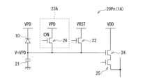
回路基板20に設けられた読出画素Prの画素回路20Prと、非読出画素Pnの画素回路20Pnとは、例えば、同じ構成を有している。画素回路20Pr,20Pnは各々、例えば、光電変換部10に接続されたFD(フローティングディフュージョン)21(第1電荷蓄積部)、リセットトランジスタ(RST)22、電位生成部23、増幅トランジスタ(AMP)24および選択トランジスタ(SEL)25を有している。本実施の形態では、光電変換部10で発生した信号電荷がFD21に蓄積される期間(後述の図6の蓄積期間T10)、画素Pのうちの一部の画素(非読出画素Pn)の画素回路20Pnでは、リセットトランジスタ22がオンされ、電位生成部23から電位VPDが第1電極11に印加される。一方、読出画素Prの画素回路20Prでは、リセットトランジスタ22がオフ状態となっている。例えば、このような、リセットトランジスタ22の動作の違いにより、読出画素Prと非読出画素Pnとが区別される。
The pixel circuit 20Pr of the readout pixel Pr provided on the
FD21では、光電変換部10(光電変換膜13)で発生した信号電荷が蓄積されるようになっている。FD21は、光電変換部10の第1電極11とともに、リセットトランジスタ22のソースおよび増幅トランジスタ24のゲートに接続されている。
The
リセットトランジスタ22は、オンされたとき、FD21にリセット電位VRSTを印加するためのものである。このリセット電位VRSTが印加されたFD21は、初期状態(リセット状態)となる。ここでは、このリセットトランジスタ22のドレインが、電位生成部23に接続されている。非読出画素Pnでは、光電変換部10で発生した信号電荷がFD21に蓄積される期間、このリセットトランジスタ22がオン状態となり、電位生成部23から第1電極11に電位VPDが印加される。リセットトランジスタ22のゲートは、制御線Lps(図3)に接続されており、リセットトランジスタ22のオンおよびオフは、制御線Lpsに制御される。
The
電位生成部23は、リセットトランジスタ22を介して光電変換部10(第1電極11)に接続されている。リセットトランジスタ22のドレインに直列に接続された電位生成部23は、リセット電位VRSTと、リセット電位VRSTとは異なる所定の電位VPDとを生成するものである。電位VPDは、例えば、光電変換部10の第2電極15に印加される電位V15と略同じ電位であり(電位VPD≒電位V15)、この電位VPDが、オン状態のリセットトランジスタ22を介して第1電極11に印加されることにより、第1電極11と第2電極15との間の電位差が略ゼロ(0)となる。電位VPDを第1電極11に印加したときの第1電極11と第2電極15との間の電位差は、第1電極11にリセット電位VRSTを印加したときの、第1電極11と第2電極15との間の電位差よりも小さくなっている(|VPD-V15|<|VRST-V15|)。The
増幅トランジスタ24のゲートはFD21に接続され、増幅トランジスタ24のドレインは電源電圧VDDに接続され、増幅トランジスタ24のソースは選択トランジスタ25のドレインに接続されている。この増幅トランジスタ24は、垂直信号線Lsigを介して接続された、定電流源としての負荷MOS(Metal Oxide Semiconductor)とソースフォロア回路を構成している。FD21の電位に応じた画素信号が、この増幅トランジスタ24から選択トランジスタ25を介して水平選択部203に出力されるようになっている。
The gate of the
選択トランジスタ25のソースは、垂直信号線Lsigに接続されている。選択トランジスタ25がオンされると、オンされた画素Pの画素信号が、垂直信号線Lsigを介して水平選択部203に出力されるようになっている。
The source of the
[撮像素子1の動作]
図5を用いて撮像素子1の動作について説明する。撮像素子1では、第2電極15および第2半導体層14を介して、光電変換膜13へ光(例えば赤外領域の波長の光)が入射すると、この光は光電変換膜13において吸収される。これにより、各画素Pの光電変換膜13では正孔(ホール)および電子の対が発生する(光電変換される)。このとき、読出画素Prでは、例えば第1電極11に所定の電位(例えばリセット電位VRST)が印加されると、第1電極11と第2電極15との間に電位勾配が生じ、発生した電荷のうち一方の電荷(例えば正孔)が、信号電荷として拡散領域12Aに移動し、拡散領域12Aから画素P毎に第1電極11へ収集される。[Operation of image sensor 1]
The operation of the
一方、非読出画素Pnでは、第1電極11に電位VPDが印加され、第1電極11と第2電極15との間の電位差が略ゼロとなる。このため、非読出画素Pnの光電変換膜13で発生した信号電荷は、近傍の読出画素Prの拡散領域12Aに移動する。この非読出画素Pnから読出画素Prに移動した信号電荷は、読出画素Prで発生した信号電荷と合算され、読出画素Prの画素回路20Prで読み出される。
On the other hand, in the non-reading pixel Pn, the potential VPD is applied to the
図6は、読出画素PrのFD21に信号電荷が蓄積される期間(蓄積期間T10)のリセットトランジスタ22、選択トランジスタ25および電位生成部23のタイミングチャートである。
FIG. 6 is a timing chart of the
まず、画素回路20Pr,20Pnの電位生成部23では、リセット電位VRSTが生成される。読出画素Prの画素回路20Prでは、リセットトランジスタ22がオンされる。これにより、FD21の電位がリセット電位VRSTとなり、FD21が初期状態となる。その後、画素回路20Prのリセットトランジスタ22は、オフ状態となる。一方、非読出画素Pnの画素回路20Pnでは、リセットトランジスタ22がオンされた後、オン状態が維持される。
First, the reset potential VRST is generated in the
続いて、画素回路20Pr,20Pnの電位生成部23は、電位VPDを生成する。その後、読出画素Prの画素回路20Prでは、選択トランジスタ25が時刻t1でオンされた後、時刻t2でオフされる。この時刻t2から信号電荷の蓄積期間T10が開始される。蓄積期間T10にわたって、画素回路20Prでは、リセットトランジスタ22のオフ状態が維持される。一方、非読出画素Pnの画素回路20Pnでは、時刻t1,t2で、リセットトランジスタ22のオン状態および選択トランジスタ25のオフ状態が維持される。これにより、蓄積期間T10では、非読出画素Pnの第1電極11に電位VPDが印加される。
Subsequently, the
蓄積期間T10の経過後、読出画素Prの画素回路20Prでは、時刻t3で選択トランジスタ25がオンされる。これにより、画素回路20PrのFD21の電位が垂直信号線Lsigを介して水平選択部203に出力され、蓄積期間T10が終了する(時刻t3)。その後、画素回路20Prの選択トランジスタ25は、時刻t4でオフされる。一方、非読出画素Pnの画素回路20Pnでは、時刻t3,t4で選択トランジスタ25のオフ状態が維持される。時刻t4の後、画素回路20Pnでは、リセットトランジスタ22がオフされる。画素回路20Pnのリセットトランジスタ22がオフされた後、画素回路20Pr,20Pnの電位生成部23は、リセット電位VRSTを生成する。
After the accumulation period T10 has elapsed, the
[撮像素子1の作用・効果]
本実施の形態の撮像素子1では、非読出画素Pnの画素回路20Pnに、電位生成部23が設けられているので、蓄積期間T10では、非読出画素Pnの第1電極11に、電位生成部23で生成された電位VPDが印加される。これにより、非読出画素Pnでは、第1電極11と第2電極15との間の電位差が小さくなり、この非読出画素Pnで発生した信号電荷は、近傍の読出画素Prの拡散領域12Aに移動する。したがって、読出画素Prの画素回路20Prからは、読出画素Prで発生した信号電荷と、非読出画素Pnで発生した信号電荷とが合算されて読み出される。[Actions and effects of the imaging device 1]
In the
複数の画素の信号電荷を加算する方法として、画素信号を読み出した後に外部で加算する方法を考え得る。しかし、この方法では、読み出しノイズも加算されてしまう。また、垂直信号線を用いる方法や、複数の画素に共通して設けられたFDを用いる方法も考え得る。しかし、これらの方法では、非読出画素および読出画素の配置の自由度が低い。また、複数の画素に共通して設けられたFDを用いる方法では、光電変換の変換効率が落ちやすい。 As a method of adding signal charges of a plurality of pixels, a method of reading pixel signals and then adding them externally can be considered. However, this method also adds read noise. A method using a vertical signal line and a method using an FD provided in common for a plurality of pixels can also be considered. However, these methods have a low degree of freedom in arranging non-readout pixels and readout pixels. Further, in the method of using an FD provided in common for a plurality of pixels, the conversion efficiency of photoelectric conversion tends to decrease.
撮像素子に、FDとは別に、加算用の信号電荷の蓄積部を設ける方法も考え得る。しかし、この方法も、非読出画素および読出画素の配置の自由度が低い。更に、加算される画素の数を大きくすると、レイアウトが複雑になる。加えて、カップリングに起因したノイズも発生しやすくなる。 It is also conceivable to provide the imaging device with a signal charge accumulation section for addition, in addition to the FD. However, this method also has a low degree of freedom in arranging non-readout pixels and readout pixels. Furthermore, increasing the number of pixels to be added complicates the layout. In addition, noise due to coupling is likely to occur.
これに対し、本実施の形態では、読出画素Prの拡散領域12Aに、非読出画素Pnの信号電荷が移動し、光電変換部10で信号電荷が加算される。したがって、ノイズは加算されにくい。また、読出画素Prおよび非読出画素Pnの配置は、制御線Lpsによって調整可能であり、読出画素Prおよび非読出画素Pnの配置は、自由に設定できる。例えば、制御線Lpsを行方向および列方向に設けることにより(後述の図17等参照)、2方向(行方向および列方向)にわたって、読出画素Prおよび非読出画素Pnを自由に配置することができる。また、加算される画素Pの数も自由に調整できる。更に、撮像素子1では、加算用の信号電荷の蓄積部が不要となるので、光電変換の変換効率も維持できる。加えて、カップリングに起因したノイズの発生も抑えられる。
In contrast, in the present embodiment, the signal charge of the non-readout pixel Pn moves to the
以上説明したように、本実施の形態では、非読出画素Pnの画素回路20Pnに、電位VPDを生成する電位生成部23を設けるようにしたので、非読出画素Pnで発生した信号電荷は、読出画素Prで発生した信号電荷とともに、読出画素Prの画素回路20Prで読みだされる。よって、複数の画素Pの信号電荷を加算可能となる。
As described above, in the present embodiment, the pixel circuit 20Pn of the non-readout pixel Pn is provided with the
また、撮像素子1では、非読出画素Pnを除き、読出画素Prのみから信号電荷が読み出されるので、高速での読み出しが可能となる。
In addition, in the
以下、他の実施の形態および変形例およびについて説明するが、以降の説明において上記第1の実施の形態と同一構成部分については同一符号を付してその説明は適宜省略する。 Other embodiments and modifications will be described below, but in the following description, the same reference numerals will be given to the same components as in the first embodiment, and the description thereof will be omitted as appropriate.
<第2の実施の形態>
図7A,図7Bは、第2の実施の形態に係る撮像素子(撮像素子1A)の画素回路20Pr,20Pnの回路構成を表したものである。この画素回路20Pr,20Pnは、光電変換部10(第1電極11)とリセットトランジスタ22との間に、リセットトランジスタ22に並列に接続された電位生成部(電位生成部23A)を有している。この点を除き、第2の実施の形態に係る撮像素子1Aは、上記第1の実施の形態の撮像素子1と同様の構成を有し、その作用および効果も同様である。<Second Embodiment>
7A and 7B show circuit configurations of pixel circuits 20Pr and 20Pn of an imaging device (
読出画素Prの画素回路20Prと、非読出画素Pnの画素回路20Pnとは、例えば、同じ構成を有している。この画素回路20Pr,20Pnの電位生成部23Aは、ドレインが電位VPDに接続されたトランジスタ26(第1トランジスタ)を含んでいる。この電位VPDが、オン状態のトランジスタ26を介して第1電極11に印加されることにより、第1電極11と第2電極15との間の電位差が略ゼロ(0)となる。本実施の形態では、光電変換部10で発生した信号電荷がFD21に蓄積される期間(後述の図8の蓄積期間T10)、非読出画素Pnの画素回路20Pnでは、トランジスタ26がオンされ、電位生成部23Aから電位VPDが第1電極11に印加される。一方、読出画素Prの画素回路20Prでは、トランジスタ26がオフされる。このような、トランジスタ26の動作の違いにより、読出画素Prと非読出画素Pnとが区別される。
The pixel circuit 20Pr of the readout pixel Pr and the pixel circuit 20Pn of the non-readout pixel Pn have, for example, the same configuration. The
トランジスタ26のソースは、FD21、リセットトランジスタ22のソースおよび増幅トランジスタ24のゲートに接続されている。トランジスタ26のゲートは、制御線Lps(図3)に接続されており、トランジスタ26のオンおよびオフは、制御線Lpsに制御される。このトランジスタ26は、蓄積期間T10以外の期間、オーバーフロートランジスタとして機能してもよい。トランジスタ26は、例えば薄膜トランジスタ(Thin Film Transistor)により構成されている。
The source of the
リセットトランジスタ22は、トランジスタ26のソースと増幅トランジスタ24のゲートとの間に、トランジスタ26に並列に接続されている。このリセットトランジスタ22のドレインは、リセット電位VRSTに接続されている。
The
図8は、読出画素PrのFD21に信号電荷が蓄積される期間(蓄積期間T10)のリセットトランジスタ22、選択トランジスタ25およびトランジスタ26(電位生成部23A)のタイミングチャートである。
FIG. 8 is a timing chart of the
まず、読出画素Prの画素回路20Prでは、リセットトランジスタ22がオンされる。これにより、FD21の電位がリセット電位VRSTとなり、FD21が初期状態となる。その後、画素回路20Prのリセットトランジスタ22は、オフ状態となる。この間、画素回路20Prのトランジスタ26は、オフ状態が維持される。一方、非読出画素Pnの画素回路20Pnでは、リセットトランジスタ22のオフ状態およびトランジスタ26のオン状態が維持される。
First, in the pixel circuit 20Pr of the readout pixel Pr, the
その後、読出画素Prの画素回路20Prでは、選択トランジスタ25が時刻t1でオンされた後、時刻t2でオフされる。この時刻t2から信号電荷の蓄積期間T10が開始される。蓄積期間T10にわたって、画素回路20Prでは、リセットトランジスタ22のオフ状態、選択トランジスタ25のオフ状態およびトランジスタ26のオフ状態が維持される。一方、非読出画素Pnの画素回路20Pnでは、時刻t1,t2で、リセットトランジスタ22のオフ状態、選択トランジスタ25のオフ状態およびトランジスタ26のオン状態が維持される。これにより、蓄積期間T10では、非読出画素Pnの第1電極11に、トランジスタ26を介して電位VPDが印加される。
Thereafter, in the pixel circuit 20Pr of the readout pixel Pr, the
蓄積期間T10の経過後、読出画素Prの画素回路20Prでは、時刻t3で選択トランジスタ25がオンされる。これにより、画素回路20PrのFD21の電位が垂直信号線Lsigを介して水平選択部203に出力され、蓄積期間T10が終了する(時刻t3)。その後、画素回路20Prの選択トランジスタ25は、時刻t4でオフされる。一方、非読出画素Pnの画素回路20Pnでは、時刻t3,t4でリセットトランジスタ22のオフ状態、選択トランジスタ25のオフ状態およびトランジスタ26のオン状態が維持される。
After the accumulation period T10 has elapsed, the
このような撮像素子1Aも、上記撮像素子1で説明したのと同様に、非読出画素Pnの画素回路20Pnに、電位生成部23Aが設けられているので、非読出画素Pnでは、第1電極11と第2電極15との間の電位差が小さくなり、この非読出画素Pnで発生した信号電荷は、近傍の読出画素Prの拡散領域12Aに移動する。したがって、読出画素Prの画素回路20Prからは、読出画素Prで発生した信号電荷と、非読出画素Pnで発生した信号電荷とが合算されて読み出される。
In such an
<変形例1>
上記第2の実施の形態では、読出画素Prの画素回路20Prと、非読出画素Pnの画素回路20Pnとが同じ構成を有している例について説明したが、これらは互いに異なる構成を有していてもよい。<
In the second embodiment described above, the pixel circuit 20Pr of the readout pixel Pr and the pixel circuit 20Pn of the non-readout pixel Pn have the same configuration, but they have different configurations. may
例えば、読出画素Pr,非読出画素Pnの配置が固定されているとき、読出画素Prの画素回路20Prの電位生成部23A(トランジスタ26)を省略するようにしてもよい。
For example, when the arrangement of the readout pixel Pr and the non-readout pixel Pn is fixed, the
図9は、電位生成部23A(トランジスタ26)を有しない画素回路20Prの構成の一例を表している。このように、電位生成部23Aに代えて、画素回路20Prが、容量切替用のトランジスタ27(第3トランジスタ)および付加容量素子28を有していてもよい。
FIG. 9 shows an example of the configuration of a pixel circuit 20Pr that does not have the
トランジスタ27は、FD21の容量を切り替えるためのものである。トランジスタ27は、例えば、光電変換部10とリセットトランジスタ22との間に、リセットトランジスタ22に並列に接続されている。トランジスタ27のソースはFD21に接続され、トランジスタ27のドレインは付加容量素子28の一端に接続されている。付加容量素子28の他端は、例えば、接地電位(GND)に接続されている。
The
トランジスタ27がオン状態となると、FD21に付加容量素子28が接続され、多量の信号電荷を蓄積可能な状態(高容量選択状態)となる。トランジスタ27がオフ状態となると、FD21と付加容量素子28とが非接続となり、少量の信号電荷を蓄積可能な状態(低容量選択状態)となる。このように、複数の画素Pの信号電荷を加算する際に、ダイナミックレンジが切り替えられるようにしてもよい。
When the
<変形例2>
図10は、上記第2の実施の形態の変形例(変形例2)に係る画素回路20Pr,20Pnの回路構成の一例を表している。この画素回路20Pr,20Pnは、光電変換部10に接続された電荷蓄積部31と、電荷蓄積部31とFD21との間に配置された転送トランジスタ32とを含むものである。このように、画素回路20Pr,20Pnに電荷蓄積部31および転送トランジスタ32を設けることにより、グローバルシャッター機能を有する撮像素子1Aを実現可能となる。<Modification 2>
FIG. 10 shows an example of the circuit configuration of pixel circuits 20Pr and 20Pn according to a modification (modification 2) of the second embodiment. The pixel circuits 20Pr and 20Pn include a
電荷蓄積部31の一端は、光電変換部10(第1電極11)および転送トランジスタ32のソースに接続されている。この電荷蓄積部31は、光電変換部10で生成された信号電荷を、一旦保持するための電荷保持部である。
One end of the
転送トランジスタ32のドレインは、FD21に接続されている。転送トランジスタ32がオンされると、電荷蓄積部31に一旦保持された信号電荷が読み出され、FD21に転送される。例えば、電位生成部23A(トランジスタ26)は、電荷蓄積部31と転送トランジスタ32との間に配置されている。
A drain of the
<第3の実施の形態>
図11A,図11Bは、第3の実施の形態に係る撮像素子(撮像素子1B)の画素回路20Pr,20Pnの回路構成を表したものである。この画素回路20Pr,20Pnは、光電変換部10(第1電極11)とFD21との間に、光電変換部10に直列に接続された電位生成部(電位生成部23B)を有している。この点を除き、第3の実施の形態に係る撮像素子1Bは、上記第1の実施の形態の撮像素子1と同様の構成を有し、その作用および効果も同様である。<Third Embodiment>
11A and 11B show circuit configurations of pixel circuits 20Pr and 20Pn of an imaging device (
読出画素Prの画素回路20Prと、非読出画素Pnの画素回路20Pnとは、例えば、同じ構成を有している。この画素回路20Pr,20Pnの電位生成部23Bは、トランジスタ29(第1トランジスタ)を含んでいる。本実施の形態では、光電変換部10で発生した信号電荷がFD21に蓄積される期間(後述の図12の蓄積期間T10)、非読出画素Pnの画素回路20Pnでは、トランジスタ29がオフされ、光電変換部10とFD21とが非接続となる。これにより、第1電極11と第2電極15との間の電位差が略ゼロ(0)となる。一方、読出画素Prの画素回路20Prでは、トランジスタ29がオン状態となり、光電変換部10とFD21とが接続される。このような、トランジスタ29の動作の違いにより、読出画素Prと非読出画素Pnとが区別される。
The pixel circuit 20Pr of the readout pixel Pr and the pixel circuit 20Pn of the non-readout pixel Pn have, for example, the same configuration. The
例えば、トランジスタ29のドレインは光電変換部10に接続され、トランジスタ29のソースはFD21に接続されている。トランジスタ29のゲートは、制御線Lps(図3)に接続されており、トランジスタ29のオンおよびオフは、制御線Lpsに制御される。トランジスタ29は、例えば薄膜トランジスタにより構成されている。
For example, the drain of the
リセットトランジスタ22は、トランジスタ29のソースと増幅トランジスタ24のゲートとの間に配置されている。このリセットトランジスタ22のドレインは、リセット電位VRSTに接続されている。
The
図12は、読出画素PrのFD21に信号電荷が蓄積される期間(蓄積期間T10)のリセットトランジスタ22、選択トランジスタ25およびトランジスタ29(電位生成部23B)のタイミングチャートである。
FIG. 12 is a timing chart of the
まず、読出画素Prの画素回路20Prでは、リセットトランジスタ22がオンされる。これにより、FD21の電位がリセット電位VRSTとなり、FD21が初期状態となる。その後、画素回路20Prのリセットトランジスタ22は、オフ状態となる。この間、画素回路20Prのトランジスタ29は、オン状態が維持される。一方、非読出画素Pnの画素回路20Pnでは、リセットトランジスタ22のオフ状態およびトランジスタ29のオフ状態が維持される。
First, in the pixel circuit 20Pr of the readout pixel Pr, the
その後、読出画素Prの画素回路20Prでは、選択トランジスタ25が時刻t1でオンされた後、時刻t2でオフされる。この時刻t2から信号電荷の蓄積期間T10が開始される。蓄積期間T10にわたって、画素回路20Prでは、リセットトランジスタ22のオフ状態、選択トランジスタ25のオフ状態およびトランジスタ29のオン状態が維持される。一方、非読出画素Pnの画素回路20Pnでは、時刻t1,t2および蓄積期間T10で、リセットトランジスタ22のオフ状態、選択トランジスタ25のオフ状態およびトランジスタ29のオフ状態が維持される。これにより、蓄積期間T10では、非読出画素Pnの第1電極11は、第2電極15と略同じ電位となる。換言すれば、非読出画素Pnの第1電極11に、電位VPDが印加される。
Thereafter, in the pixel circuit 20Pr of the readout pixel Pr, the
蓄積期間T10の経過後、読出画素Prの画素回路20Prでは、時刻t3で選択トランジスタ25がオンされる。これにより、画素回路20PrのFD21の電位が垂直信号線Lsigを介して水平選択部203に出力され、蓄積期間T10が終了する(時刻t3)。その後、画素回路20Prの選択トランジスタ25は、時刻t4でオフされる。一方、非読出画素Pnの画素回路20Pnでは、時刻t3,t4でリセットトランジスタ22のオフ状態、選択トランジスタ25のオフ状態およびトランジスタ29のオフ状態が維持される。
After the accumulation period T10 has elapsed, the
このような撮像素子1Bも、上記撮像素子1で説明したのと同様に、非読出画素Pnの画素回路20Pnに、電位生成部23Bが設けられているので、非読出画素Pnでは、第1電極11と第2電極15との間の電位差が小さくなり、この非読出画素Pnで発生した信号電荷は、近傍の読出画素Prの拡散領域12Aに移動する。したがって、読出画素Prの画素回路20Prからは、読出画素Prで発生した信号電荷と、非読出画素Pnで発生した信号電荷とが合算されて読み出される。
In such an
この読出画素Prの画素回路20Prおよび非読出画素Pnの画素回路20Pnは、上記変形例1で説明したように、互いに異なる構成を有していてもよい。
The pixel circuit 20Pr of the readout pixel Pr and the pixel circuit 20Pn of the non-readout pixel Pn may have configurations different from each other, as described in
例えば、読出画素Pr,非読出画素Pnの配置が固定されているとき、読出画素Prの画素回路20Prの電位生成部23B(トランジスタ29)を省略するようにしてもよい。この画素回路20Prには、電位生成部23Bに代えて、容量切替用のトランジスタ27および付加容量素子28を設けるようにしてもよい。
For example, when the arrangement of the readout pixel Pr and the non-readout pixel Pn is fixed, the
図13は、上記第3の実施の形態で説明した画素回路20Pr,20Pnの他の例を表している。この画素回路20Pr,20Pnは、上記変形例2で説明したのと同様に、電荷蓄積部31と、転送トランジスタ32を含むものである。このように、画素回路20Pr,20Pnに電荷蓄積部31および転送トランジスタ32を設けることにより、グローバルシャッター機能を有する撮像素子1Bを実現可能となる。電荷蓄積部31は、電位生成部23B(トランジスタ29)を介して光電変換部10に接続されている。
FIG. 13 shows another example of the pixel circuits 20Pr and 20Pn described in the third embodiment. The pixel circuits 20Pr and 20Pn each include a
<第4の実施の形態>
図14A,図14Bは、第4の実施の形態に係る撮像素子(撮像素子1C)の画素回路20Pr,20Pnの回路構成を表したものである。撮像素子1Cはグローバルシャッター機能を有する撮像素子であり、画素回路20Pr,20Pnの電位生成部(電位生成部23C)は、画素P毎に設けられた電荷蓄積部31(第2電荷蓄積部)と、電荷蓄積部31とFD21との間に設けられた転送トランジスタ32(第2トランジスタ)とを含んでいる。この点を除き、第4の実施の形態に係る撮像素子1Cは、上記第1の実施の形態の撮像素子1と同様の構成を有し、その作用および効果も同様である。<Fourth Embodiment>
14A and 14B show circuit configurations of pixel circuits 20Pr and 20Pn of an imaging device (
読出画素Prの画素回路20Prと、非読出画素Pnの画素回路20Pnとは、例えば、同じ構成を有している。本実施の形態では、光電変換部10で発生した信号電荷がFD21に蓄積される期間(後述の図15の蓄積期間T10)、非読出画素Pnの画素回路20Pnでは、転送トランジスタ32がオフ状態となり、電荷蓄積部31とFD21とが非接続となる。これにより、電荷蓄積部31に信号電荷が蓄積されていくと、第1電極11と第2電極15との間の電位差が略ゼロ(0)となる。一方、読出画素Prの画素回路20Prでは、転送トランジスタ32が通常駆動され、蓄積期間T10内に、電荷蓄積部31からFD21へと信号電荷が転送される。このような、転送トランジスタ32の動作の違いにより、読出画素Prと非読出画素Pnとが区別される。
The pixel circuit 20Pr of the readout pixel Pr and the pixel circuit 20Pn of the non-readout pixel Pn have, for example, the same configuration. In the present embodiment, the
電荷蓄積部31は、光電変換部10(第1電極11)とFD21との間に設けられている。上記変形例2で説明したのと同様に、電荷蓄積部31の一端は、光電変換部10(第1電極11)および転送トランジスタ32のソースに接続されている。転送トランジスタ32のドレインは、FD21に接続されている。
The
リセットトランジスタ22のソースは、転送トランジスタ32のドレイン、FD21および増幅トランジスタ24のゲートに接続されている。リセットトランジスタ22のドレインは、リセット電位VRSTに接続されている。
The source of the
図15は、読出画素PrのFD21に信号電荷が蓄積される期間(蓄積期間T10)のリセットトランジスタ22、選択トランジスタ25および転送トランジスタ32のタイミングチャートである。
FIG. 15 is a timing chart of the
まず、読出画素Prの画素回路20Prでは、リセットトランジスタ22および転送トランジスタ32が同時にオンされる。これにより、FD21および電荷蓄積部31の電位がリセット電位VRSTとなり、FD21および電荷蓄積部31が初期状態となる。その後、時刻t5で、画素回路20Prのリセットトランジスタ22および転送トランジスタ32は、同時にオフ状態となる。この時刻t5から信号電荷の蓄積期間T10が開始される。その後、読出画素Prの画素回路20Prでは、選択トランジスタ25が時刻t6でオンされた後、時刻t7でオフされる。一方、非読出画素Pnの画素回路20Pnでは、時刻t5から時刻t7にわたって、リセットトランジスタ22のオフ状態、選択トランジスタ25のオフ状態および転送トランジスタ32のオフ状態が維持される。
First, in the pixel circuit 20Pr of the readout pixel Pr, the
蓄積期間T10の終了間際に、画素回路20Prでは、転送トランジスタ32がオンされる。これにより、画素回路20Prの電荷蓄積部31の電位が、転送トランジスタ32を介してFD21に出力される。この後、時刻t8で転送トランジスタ32はオフされ、選択トランジスタ25がオンされる。これにより、画素回路20PrのFD21の電位が垂直信号線Lsigを介して水平選択部203に出力され、蓄積期間T10が終了する(時刻t8)。その後、画素回路20Prの選択トランジスタ25は、時刻t9でオフされる。
Just before the end of the accumulation period T10, the
一方、非読出画素Pnの画素回路20Pnでは、蓄積期間T10およびその経過後にわたって、リセットトランジスタ22のオフ状態、選択トランジスタ25のオフ状態および転送トランジスタ32のオフ状態が維持される。これにより、蓄積期間T10では、非読出画素Pnの第1電極11は、第2電極15と略同じ電位となる。換言すれば、非読出画素Pnの第1電極11に、電位VPDが印加される。
On the other hand, in the pixel circuit 20Pn of the non-reading pixel Pn, the off state of the
このような撮像素子1Cも、上記撮像素子1で説明したのと同様に、非読出画素Pnの画素回路20Pnに、電位生成部23Cが設けられているので、非読出画素Pnでは、第1電極11と第2電極15との間の電位差が小さくなり、この非読出画素Pnで発生した信号電荷は、近傍の読出画素Prの拡散領域12Aに移動する。したがって、読出画素Prの画素回路20Prからは、読出画素Prで発生した信号電荷と、非読出画素Pnで発生した信号電荷とが合算されて読み出される。
In the
<変形例3>
上述の図2では、読出画素Prおよび非読出画素Pnを画素P行毎に、交互に配置する例を示したが、読出画素Prおよび非読出画素Pnは自由に配置することが可能である。例えば、図示は省略するが、読出画素Prおよび非読出画素Pnを画素Pの列毎に、交互に配置するようにしてもよい。<
Although FIG. 2 described above shows an example in which the readout pixels Pr and the non-readout pixels Pn are arranged alternately for each pixel P row, the readout pixels Pr and the non-readout pixels Pn can be arranged freely. For example, although not shown, the readout pixels Pr and the non-readout pixels Pn may be arranged alternately for each column of the pixels P. FIG.
例えば、図16A,図16Bに示したように、2行または3行の画素P行毎に読出画素Prの行を配置するようにしてもよい。このとき、列方向に隣り合う3つまたは4つの画素Pの信号電荷が加算される。4行以上の画素P行毎に読出画素Prの行を配置するようにしてもよい。2列、3列または4列以上の画素P列毎に読出画素Prの行を配置するようにしてもよい。 For example, as shown in FIGS. 16A and 16B, a row of readout pixels Pr may be arranged every two or three pixel P rows. At this time, signal charges of three or four pixels P adjacent in the column direction are added. A row of readout pixels Pr may be arranged for every four or more pixel P rows. A row of readout pixels Pr may be arranged for every two, three, or four or more pixel P columns.
図17は、読出画素Prおよび非読出画素Pnの配置の一例を表している。このように、2行×2列の画素Pに1つの読出画素Prを配置するようにしてもよい。このとき、4つ(2行×2列)の画素Pの信号電荷が加算される。 FIG. 17 shows an example of the arrangement of readout pixels Pr and non-readout pixels Pn. In this manner, one readout pixel Pr may be arranged for pixels P arranged in two rows and two columns. At this time, the signal charges of four (2 rows×2 columns) pixels P are added.
図18は、図17の読出画素Prおよび非読出画素Pnに接続された制御線(制御線Lps1,Lps2)の構成の一例を表している。撮像素子1,1A,1B,1Cは、例えば、行方向に延在する複数の制御線Lps1と、列方向に延在する複数の制御線Lps2とを有している。
FIG. 18 shows an example of the configuration of control lines (control lines Lps1 and Lps2) connected to the readout pixel Pr and the non-readout pixel Pn in FIG. The
図19および図20は、図17の読出画素Prおよび非読出画素Pnに設けられた画素回路20Pr,20Pnの回路構成の一例を表している。例えば、上記第1の実施の形態で説明した撮像素子1の画素回路20Pr,20Pn(図4参照)は、例えば、制御線Lps1に接続されたリセットトランジスタ22Aと、制御線Lps2に接続されたリセットトランジスタ22Bとを有している(図19)。上記第2の実施の形態で説明した撮像素子2の画素回路20Pr,20Pn(図7A,図7B参照)は、例えば、制御線Lps1に接続されたトランジスタ26Aと、制御線Lps2に接続されたトランジスタ26Bとを有している(図20)。
19 and 20 show an example of circuit configurations of pixel circuits 20Pr and 20Pn provided in the readout pixel Pr and the non-readout pixel Pn of FIG. For example, the pixel circuits 20Pr and 20Pn (see FIG. 4) of the
図21A,図21Bに示したように、3行×3列または4行×4列の画素Pに1つの読出画素Prを配置するようにしてもよい。5行×5列以上の画素Pに1つの読出画素Prを配置するようにしてもよい。例えば、100μm×100μmの領域内に配置された複数の画素Pの信号電荷を加算することが可能である。 As shown in FIGS. 21A and 21B, one readout pixel Pr may be arranged in pixels P of 3 rows×3 columns or 4 rows×4 columns. One readout pixel Pr may be arranged for pixels P of 5 rows×5 columns or more. For example, it is possible to add the signal charges of a plurality of pixels P arranged in an area of 100 μm×100 μm.
<適用例>
上述の撮像素子1,1A,1B,1Cは、例えば赤外領域を撮像可能なカメラなど、様々なタイプの撮像装置(電子機器)に適用することができる。図22に、その一例として、電子機器3(カメラ)の概略構成を示す。この電子機器3は、例えば静止画または動画を撮影可能なカメラであり、撮像素子1,1A,1B,1Cと、光学系(光学レンズ)310と、シャッタ装置311と、撮像素子1,1A,1B,1Cおよびシャッタ装置311を駆動する駆動部313と、信号処理部312とを有する。<Application example>
The
光学系310は、被写体からの像光(入射光)を撮像素子1,1A,1B,1Cへ導くものである。この光学系310は、複数の光学レンズから構成されていてもよい。シャッタ装置311は、撮像素子1,1A,1B,1Cへの光照射期間および遮光期間を制御するものである。駆動部313は、撮像素子1,1A,1B,1Cの転送動作およびシャッタ装置311のシャッタ動作を制御するものである。信号処理部312は、撮像素子1,1A,1B,1Cから出力された信号に対し、各種の信号処理を行うものである。信号処理後の映像信号Doutは、メモリなどの記憶媒体に記憶されるか、あるいは、モニタ等に出力される。
The
<体内情報取得システムへの応用例>
更に、本開示に係る技術(本技術)は、様々な製品へ応用することができる。例えば、本開示に係る技術は、内視鏡手術システムに適用されてもよい。<Example of application to in-vivo information acquisition system>
Furthermore, the technology (this technology) according to the present disclosure can be applied to various products. For example, the technology according to the present disclosure may be applied to an endoscopic surgery system.
図23は、本開示に係る技術(本技術)が適用され得る、カプセル型内視鏡を用いた患者の体内情報取得システムの概略的な構成の一例を示すブロック図である。 FIG. 23 is a block diagram showing an example of a schematic configuration of a system for acquiring in-vivo information of a patient using a capsule endoscope, to which the technology (present technology) according to the present disclosure can be applied.
体内情報取得システム10001は、カプセル型内視鏡10100と、外部制御装置10200とから構成される。
An in-vivo
カプセル型内視鏡10100は、検査時に、患者によって飲み込まれる。カプセル型内視鏡10100は、撮像機能及び無線通信機能を有し、患者から自然排出されるまでの間、胃や腸等の臓器の内部を蠕動運動等によって移動しつつ、当該臓器の内部の画像(以下、体内画像ともいう)を所定の間隔で順次撮像し、その体内画像についての情報を体外の外部制御装置10200に順次無線送信する。
The
外部制御装置10200は、体内情報取得システム10001の動作を統括的に制御する。また、外部制御装置10200は、カプセル型内視鏡10100から送信されてくる体内画像についての情報を受信し、受信した体内画像についての情報に基づいて、表示装置(図示せず)に当該体内画像を表示するための画像データを生成する。
The
体内情報取得システム10001では、このようにして、カプセル型内視鏡10100が飲み込まれてから排出されるまでの間、患者の体内の様子を撮像した体内画像を随時得ることができる。
In this manner, the in-vivo
カプセル型内視鏡10100と外部制御装置10200の構成及び機能についてより詳細に説明する。
The configurations and functions of the
カプセル型内視鏡10100は、カプセル型の筐体10101を有し、その筐体10101内には、光源部10111、撮像部10112、画像処理部10113、無線通信部10114、給電部10115、電源部10116、及び制御部10117が収納されている。
A
光源部10111は、例えばLED(light emitting diode)等の光源から構成され、撮像部10112の撮像視野に対して光を照射する。
The
撮像部10112は、撮像素子、及び当該撮像素子の前段に設けられる複数のレンズからなる光学系から構成される。観察対象である体組織に照射された光の反射光(以下、観察光という)は、当該光学系によって集光され、当該撮像素子に入射する。撮像部10112では、撮像素子において、そこに入射した観察光が光電変換され、その観察光に対応する画像信号が生成される。撮像部10112によって生成された画像信号は、画像処理部10113に提供される。
The
画像処理部10113は、CPU(Central Processing Unit)やGPU(Graphics Processing Unit)等のプロセッサによって構成され、撮像部10112によって生成された画像信号に対して各種の信号処理を行う。画像処理部10113は、信号処理を施した画像信号を、RAWデータとして無線通信部10114に提供する。
The
無線通信部10114は、画像処理部10113によって信号処理が施された画像信号に対して変調処理等の所定の処理を行い、その画像信号を、アンテナ10114Aを介して外部制御装置10200に送信する。また、無線通信部10114は、外部制御装置10200から、カプセル型内視鏡10100の駆動制御に関する制御信号を、アンテナ10114Aを介して受信する。無線通信部10114は、外部制御装置10200から受信した制御信号を制御部10117に提供する。
給電部10115は、受電用のアンテナコイル、当該アンテナコイルに発生した電流から電力を再生する電力再生回路、及び昇圧回路等から構成される。給電部10115では、いわゆる非接触充電の原理を用いて電力が生成される。
The
電源部10116は、二次電池によって構成され、給電部10115によって生成された電力を蓄電する。図23では、図面が煩雑になることを避けるために、電源部10116からの電力の供給先を示す矢印等の図示を省略しているが、電源部10116に蓄電された電力は、光源部10111、撮像部10112、画像処理部10113、無線通信部10114、及び制御部10117に供給され、これらの駆動に用いられ得る。
The
制御部10117は、CPU等のプロセッサによって構成され、光源部10111、撮像部10112、画像処理部10113、無線通信部10114、及び、給電部10115の駆動を、外部制御装置10200から送信される制御信号に従って適宜制御する。
The
外部制御装置10200は、CPU,GPU等のプロセッサ、又はプロセッサとメモリ等の記憶素子が混載されたマイクロコンピュータ若しくは制御基板等で構成される。外部制御装置10200は、カプセル型内視鏡10100の制御部10117に対して制御信号を、アンテナ10200Aを介して送信することにより、カプセル型内視鏡10100の動作を制御する。カプセル型内視鏡10100では、例えば、外部制御装置10200からの制御信号により、光源部10111における観察対象に対する光の照射条件が変更され得る。また、外部制御装置10200からの制御信号により、撮像条件(例えば、撮像部10112におけるフレームレート、露出値等)が変更され得る。また、外部制御装置10200からの制御信号により、画像処理部10113における処理の内容や、無線通信部10114が画像信号を送信する条件(例えば、送信間隔、送信画像数等)が変更されてもよい。
The
また、外部制御装置10200は、カプセル型内視鏡10100から送信される画像信号に対して、各種の画像処理を施し、撮像された体内画像を表示装置に表示するための画像データを生成する。当該画像処理としては、例えば現像処理(デモザイク処理)、高画質化処理(帯域強調処理、超解像処理、NR(Noise reduction)処理及び/又は手ブレ補正処理等)、並びに/又は拡大処理(電子ズーム処理)等、各種の信号処理を行うことができる。外部制御装置10200は、表示装置の駆動を制御して、生成した画像データに基づいて撮像された体内画像を表示させる。あるいは、外部制御装置10200は、生成した画像データを記録装置(図示せず)に記録させたり、印刷装置(図示せず)に印刷出力させてもよい。
The
以上、本開示に係る技術が適用され得る体内情報取得システムの一例について説明した。本開示に係る技術は、以上説明した構成のうち、例えば、撮像部10112に適用され得る。これにより、検出精度が向上する。
An example of an in-vivo information acquisition system to which the technology according to the present disclosure can be applied has been described above. The technology according to the present disclosure can be applied to, for example, the
<内視鏡手術システムへの応用例>
本開示に係る技術(本技術)は、様々な製品へ応用することができる。例えば、本開示に係る技術は、内視鏡手術システムに適用されてもよい。<Example of application to an endoscopic surgery system>
The technology (the present technology) according to the present disclosure can be applied to various products. For example, the technology according to the present disclosure may be applied to an endoscopic surgery system.
図24は、本開示に係る技術(本技術)が適用され得る内視鏡手術システムの概略的な構成の一例を示す図である。 FIG. 24 is a diagram showing an example of a schematic configuration of an endoscopic surgery system to which the technique (the present technique) according to the present disclosure can be applied.
図24では、術者(医師)11131が、内視鏡手術システム11000を用いて、患者ベッド11133上の患者11132に手術を行っている様子が図示されている。図示するように、内視鏡手術システム11000は、内視鏡11100と、気腹チューブ11111やエネルギー処置具11112等の、その他の術具11110と、内視鏡11100を支持する支持アーム装置11120と、内視鏡下手術のための各種の装置が搭載されたカート11200と、から構成される。
FIG. 24 shows an operator (physician) 11131 performing surgery on a
内視鏡11100は、先端から所定の長さの領域が患者11132の体腔内に挿入される鏡筒11101と、鏡筒11101の基端に接続されるカメラヘッド11102と、から構成される。図示する例では、硬性の鏡筒11101を有するいわゆる硬性鏡として構成される内視鏡11100を図示しているが、内視鏡11100は、軟性の鏡筒を有するいわゆる軟性鏡として構成されてもよい。
An
鏡筒11101の先端には、対物レンズが嵌め込まれた開口部が設けられている。内視鏡11100には光源装置11203が接続されており、当該光源装置11203によって生成された光が、鏡筒11101の内部に延設されるライトガイドによって当該鏡筒の先端まで導光され、対物レンズを介して患者11132の体腔内の観察対象に向かって照射される。なお、内視鏡11100は、直視鏡であってもよいし、斜視鏡又は側視鏡であってもよい。
The tip of the
カメラヘッド11102の内部には光学系及び撮像素子が設けられており、観察対象からの反射光(観察光)は当該光学系によって当該撮像素子に集光される。当該撮像素子によって観察光が光電変換され、観察光に対応する電気信号、すなわち観察像に対応する画像信号が生成される。当該画像信号は、RAWデータとしてカメラコントロールユニット(CCU: Camera Control Unit)11201に送信される。
An optical system and an imaging element are provided inside the
CCU11201は、CPU(Central Processing Unit)やGPU(Graphics Processing Unit)等によって構成され、内視鏡11100及び表示装置11202の動作を統括的に制御する。さらに、CCU11201は、カメラヘッド11102から画像信号を受け取り、その画像信号に対して、例えば現像処理(デモザイク処理)等の、当該画像信号に基づく画像を表示するための各種の画像処理を施す。
The
表示装置11202は、CCU11201からの制御により、当該CCU11201によって画像処理が施された画像信号に基づく画像を表示する。
The
光源装置11203は、例えばLED(light emitting diode)等の光源から構成され、術部等を撮影する際の照射光を内視鏡11100に供給する。
The
入力装置11204は、内視鏡手術システム11000に対する入力インタフェースである。ユーザは、入力装置11204を介して、内視鏡手術システム11000に対して各種の情報の入力や指示入力を行うことができる。例えば、ユーザは、内視鏡11100による撮像条件(照射光の種類、倍率及び焦点距離等)を変更する旨の指示等を入力する。
処置具制御装置11205は、組織の焼灼、切開又は血管の封止等のためのエネルギー処置具11112の駆動を制御する。気腹装置11206は、内視鏡11100による視野の確保及び術者の作業空間の確保の目的で、患者11132の体腔を膨らめるために、気腹チューブ11111を介して当該体腔内にガスを送り込む。レコーダ11207は、手術に関する各種の情報を記録可能な装置である。プリンタ11208は、手術に関する各種の情報を、テキスト、画像又はグラフ等各種の形式で印刷可能な装置である。
The treatment
なお、内視鏡11100に術部を撮影する際の照射光を供給する光源装置11203は、例えばLED、レーザ光源又はこれらの組み合わせによって構成される白色光源から構成することができる。RGBレーザ光源の組み合わせにより白色光源が構成される場合には、各色(各波長)の出力強度及び出力タイミングを高精度に制御することができるため、光源装置11203において撮像画像のホワイトバランスの調整を行うことができる。また、この場合には、RGBレーザ光源それぞれからのレーザ光を時分割で観察対象に照射し、その照射タイミングに同期してカメラヘッド11102の撮像素子の駆動を制御することにより、RGBそれぞれに対応した画像を時分割で撮像することも可能である。当該方法によれば、当該撮像素子にカラーフィルタを設けなくても、カラー画像を得ることができる。
The
また、光源装置11203は、出力する光の強度を所定の時間ごとに変更するようにその駆動が制御されてもよい。その光の強度の変更のタイミングに同期してカメラヘッド11102の撮像素子の駆動を制御して時分割で画像を取得し、その画像を合成することにより、いわゆる黒つぶれ及び白とびのない高ダイナミックレンジの画像を生成することができる。
Further, the driving of the
また、光源装置11203は、特殊光観察に対応した所定の波長帯域の光を供給可能に構成されてもよい。特殊光観察では、例えば、体組織における光の吸収の波長依存性を利用して、通常の観察時における照射光(すなわち、白色光)に比べて狭帯域の光を照射することにより、粘膜表層の血管等の所定の組織を高コントラストで撮影する、いわゆる狭帯域光観察(Narrow Band Imaging)が行われる。あるいは、特殊光観察では、励起光を照射することにより発生する蛍光により画像を得る蛍光観察が行われてもよい。蛍光観察では、体組織に励起光を照射し当該体組織からの蛍光を観察すること(自家蛍光観察)、又はインドシアニングリーン(ICG)等の試薬を体組織に局注するとともに当該体組織にその試薬の蛍光波長に対応した励起光を照射し蛍光像を得ること等を行うことができる。光源装置11203は、このような特殊光観察に対応した狭帯域光及び/又は励起光を供給可能に構成され得る。
Also, the
図25は、図24に示すカメラヘッド11102及びCCU11201の機能構成の一例を示すブロック図である。
FIG. 25 is a block diagram showing an example of functional configurations of the
カメラヘッド11102は、レンズユニット11401と、撮像部11402と、駆動部11403と、通信部11404と、カメラヘッド制御部11405と、を有する。CCU11201は、通信部11411と、画像処理部11412と、制御部11413と、を有する。カメラヘッド11102とCCU11201とは、伝送ケーブル11400によって互いに通信可能に接続されている。
The
レンズユニット11401は、鏡筒11101との接続部に設けられる光学系である。鏡筒11101の先端から取り込まれた観察光は、カメラヘッド11102まで導光され、当該レンズユニット11401に入射する。レンズユニット11401は、ズームレンズ及びフォーカスレンズを含む複数のレンズが組み合わされて構成される。
A
撮像部11402を構成する撮像素子は、1つ(いわゆる単板式)であってもよいし、複数(いわゆる多板式)であってもよい。撮像部11402が多板式で構成される場合には、例えば各撮像素子によってRGBそれぞれに対応する画像信号が生成され、それらが合成されることによりカラー画像が得られてもよい。あるいは、撮像部11402は、3D(dimensional)表示に対応する右目用及び左目用の画像信号をそれぞれ取得するための1対の撮像素子を有するように構成されてもよい。3D表示が行われることにより、術者11131は術部における生体組織の奥行きをより正確に把握することが可能になる。なお、撮像部11402が多板式で構成される場合には、各撮像素子に対応して、レンズユニット11401も複数系統設けられ得る。
The imaging device constituting the
また、撮像部11402は、必ずしもカメラヘッド11102に設けられなくてもよい。例えば、撮像部11402は、鏡筒11101の内部に、対物レンズの直後に設けられてもよい。
Also, the
駆動部11403は、アクチュエータによって構成され、カメラヘッド制御部11405からの制御により、レンズユニット11401のズームレンズ及びフォーカスレンズを光軸に沿って所定の距離だけ移動させる。これにより、撮像部11402による撮像画像の倍率及び焦点が適宜調整され得る。
The
通信部11404は、CCU11201との間で各種の情報を送受信するための通信装置によって構成される。通信部11404は、撮像部11402から得た画像信号をRAWデータとして伝送ケーブル11400を介してCCU11201に送信する。
The
また、通信部11404は、CCU11201から、カメラヘッド11102の駆動を制御するための制御信号を受信し、カメラヘッド制御部11405に供給する。当該制御信号には、例えば、撮像画像のフレームレートを指定する旨の情報、撮像時の露出値を指定する旨の情報、並びに/又は撮像画像の倍率及び焦点を指定する旨の情報等、撮像条件に関する情報が含まれる。
Also, the
なお、上記のフレームレートや露出値、倍率、焦点等の撮像条件は、ユーザによって適宜指定されてもよいし、取得された画像信号に基づいてCCU11201の制御部11413によって自動的に設定されてもよい。後者の場合には、いわゆるAE(Auto Exposure)機能、AF(Auto Focus)機能及びAWB(Auto White Balance)機能が内視鏡11100に搭載されていることになる。
Note that the imaging conditions such as the frame rate, exposure value, magnification, and focus may be appropriately designated by the user, or may be automatically set by the
カメラヘッド制御部11405は、通信部11404を介して受信したCCU11201からの制御信号に基づいて、カメラヘッド11102の駆動を制御する。
The camera
通信部11411は、カメラヘッド11102との間で各種の情報を送受信するための通信装置によって構成される。通信部11411は、カメラヘッド11102から、伝送ケーブル11400を介して送信される画像信号を受信する。
The
また、通信部11411は、カメラヘッド11102に対して、カメラヘッド11102の駆動を制御するための制御信号を送信する。画像信号や制御信号は、電気通信や光通信等によって送信することができる。
The
画像処理部11412は、カメラヘッド11102から送信されたRAWデータである画像信号に対して各種の画像処理を施す。
The
制御部11413は、内視鏡11100による術部等の撮像、及び、術部等の撮像により得られる撮像画像の表示に関する各種の制御を行う。例えば、制御部11413は、カメラヘッド11102の駆動を制御するための制御信号を生成する。
The
また、制御部11413は、画像処理部11412によって画像処理が施された画像信号に基づいて、術部等が映った撮像画像を表示装置11202に表示させる。この際、制御部11413は、各種の画像認識技術を用いて撮像画像内における各種の物体を認識してもよい。例えば、制御部11413は、撮像画像に含まれる物体のエッジの形状や色等を検出することにより、鉗子等の術具、特定の生体部位、出血、エネルギー処置具11112の使用時のミスト等を認識することができる。制御部11413は、表示装置11202に撮像画像を表示させる際に、その認識結果を用いて、各種の手術支援情報を当該術部の画像に重畳表示させてもよい。手術支援情報が重畳表示され、術者11131に提示されることにより、術者11131の負担を軽減することや、術者11131が確実に手術を進めることが可能になる。
In addition, the
カメラヘッド11102及びCCU11201を接続する伝送ケーブル11400は、電気信号の通信に対応した電気信号ケーブル、光通信に対応した光ファイバ、又はこれらの複合ケーブルである。
A
ここで、図示する例では、伝送ケーブル11400を用いて有線で通信が行われていたが、カメラヘッド11102とCCU11201との間の通信は無線で行われてもよい。
Here, in the illustrated example, wired communication is performed using the
以上、本開示に係る技術が適用され得る内視鏡手術システムの一例について説明した。本開示に係る技術は、以上説明した構成のうち、撮像部11402に適用され得る。撮像部11402に本開示に係る技術を適用することにより、検出精度が向上する。
An example of an endoscopic surgery system to which the technology according to the present disclosure can be applied has been described above. The technology according to the present disclosure can be applied to the
なお、ここでは、一例として内視鏡手術システムについて説明したが、本開示に係る技術は、その他、例えば、顕微鏡手術システム等に適用されてもよい。 Although the endoscopic surgery system has been described as an example here, the technology according to the present disclosure may also be applied to, for example, a microsurgery system.
<移動体への応用例>
本開示に係る技術は、様々な製品へ応用することができる。例えば、本開示に係る技術は、自動車、電気自動車、ハイブリッド電気自動車、自動二輪車、自転車、パーソナルモビリティ、飛行機、ドローン、船舶、ロボット、建設機械、農業機械(トラクター)などのいずれかの種類の移動体に搭載される装置として実現されてもよい。<Example of application to a moving body>
The technology according to the present disclosure can be applied to various products. For example, the technology according to the present disclosure can be applied to any type of movement such as automobiles, electric vehicles, hybrid electric vehicles, motorcycles, bicycles, personal mobility, airplanes, drones, ships, robots, construction machinery, agricultural machinery (tractors), etc. It may also be implemented as a body-mounted device.
図26は、本開示に係る技術が適用され得る移動体制御システムの一例である車両制御システムの概略的な構成例を示すブロック図である。 FIG. 26 is a block diagram showing a schematic configuration example of a vehicle control system, which is an example of a mobile control system to which the technology according to the present disclosure can be applied.
車両制御システム12000は、通信ネットワーク12001を介して接続された複数の電子制御ユニットを備える。図26に示した例では、車両制御システム12000は、駆動系制御ユニット12010、ボディ系制御ユニット12020、車外情報検出ユニット12030、車内情報検出ユニット12040、及び統合制御ユニット12050を備える。また、統合制御ユニット12050の機能構成として、マイクロコンピュータ12051、音声画像出力部12052、及び車載ネットワークI/F(interface)12053が図示されている。
駆動系制御ユニット12010は、各種プログラムにしたがって車両の駆動系に関連する装置の動作を制御する。例えば、駆動系制御ユニット12010は、内燃機関又は駆動用モータ等の車両の駆動力を発生させるための駆動力発生装置、駆動力を車輪に伝達するための駆動力伝達機構、車両の舵角を調節するステアリング機構、及び、車両の制動力を発生させる制動装置等の制御装置として機能する。
Drive
ボディ系制御ユニット12020は、各種プログラムにしたがって車体に装備された各種装置の動作を制御する。例えば、ボディ系制御ユニット12020は、キーレスエントリシステム、スマートキーシステム、パワーウィンドウ装置、あるいは、ヘッドランプ、バックランプ、ブレーキランプ、ウィンカー又はフォグランプ等の各種ランプの制御装置として機能する。この場合、ボディ系制御ユニット12020には、鍵を代替する携帯機から発信される電波又は各種スイッチの信号が入力され得る。ボディ系制御ユニット12020は、これらの電波又は信号の入力を受け付け、車両のドアロック装置、パワーウィンドウ装置、ランプ等を制御する。
Body
車外情報検出ユニット12030は、車両制御システム12000を搭載した車両の外部の情報を検出する。例えば、車外情報検出ユニット12030には、撮像部12031が接続される。車外情報検出ユニット12030は、撮像部12031に車外の画像を撮像させるとともに、撮像された画像を受信する。車外情報検出ユニット12030は、受信した画像に基づいて、人、車、障害物、標識又は路面上の文字等の物体検出処理又は距離検出処理を行ってもよい。
External
撮像部12031は、光を受光し、その光の受光量に応じた電気信号を出力する光センサである。撮像部12031は、電気信号を画像として出力することもできるし、測距の情報として出力することもできる。また、撮像部12031が受光する光は、可視光であっても良いし、赤外線等の非可視光であっても良い。
The
車内情報検出ユニット12040は、車内の情報を検出する。車内情報検出ユニット12040には、例えば、運転者の状態を検出する運転者状態検出部12041が接続される。運転者状態検出部12041は、例えば運転者を撮像するカメラを含み、車内情報検出ユニット12040は、運転者状態検出部12041から入力される検出情報に基づいて、運転者の疲労度合い又は集中度合いを算出してもよいし、運転者が居眠りをしていないかを判別してもよい。
The vehicle interior
マイクロコンピュータ12051は、車外情報検出ユニット12030又は車内情報検出ユニット12040で取得される車内外の情報に基づいて、駆動力発生装置、ステアリング機構又は制動装置の制御目標値を演算し、駆動系制御ユニット12010に対して制御指令を出力することができる。例えば、マイクロコンピュータ12051は、車両の衝突回避あるいは衝撃緩和、車間距離に基づく追従走行、車速維持走行、車両の衝突警告、又は車両のレーン逸脱警告等を含むADAS(Advanced Driver Assistance System)の機能実現を目的とした協調制御を行うことができる。
The
また、マイクロコンピュータ12051は、車外情報検出ユニット12030又は車内情報検出ユニット12040で取得される車両の周囲の情報に基づいて駆動力発生装置、ステアリング機構又は制動装置等を制御することにより、運転者の操作に拠らずに自律的に走行する自動運転等を目的とした協調制御を行うことができる。
In addition, the
また、マイクロコンピュータ12051は、車外情報検出ユニット12030で取得される車外の情報に基づいて、ボディ系制御ユニット12020に対して制御指令を出力することができる。例えば、マイクロコンピュータ12051は、車外情報検出ユニット12030で検知した先行車又は対向車の位置に応じてヘッドランプを制御し、ハイビームをロービームに切り替える等の防眩を図ることを目的とした協調制御を行うことができる。
Further, the
音声画像出力部12052は、車両の搭乗者又は車外に対して、視覚的又は聴覚的に情報を通知することが可能な出力装置へ音声及び画像のうちの少なくとも一方の出力信号を送信する。図26の例では、出力装置として、オーディオスピーカ12061、表示部12062及びインストルメントパネル12063が例示されている。表示部12062は、例えば、オンボードディスプレイ及びヘッドアップディスプレイの少なくとも一つを含んでいてもよい。
The audio/
図27は、撮像部12031の設置位置の例を示す図である。
FIG. 27 is a diagram showing an example of the installation position of the
図27では、撮像部12031として、撮像部12101,12102,12103,12104,12105を有する。
In FIG. 27 ,
撮像部12101,12102,12103,12104,12105は、例えば、車両12100のフロントノーズ、サイドミラー、リアバンパ、バックドア及び車室内のフロントガラスの上部等の位置に設けられる。フロントノーズに備えられる撮像部12101及び車室内のフロントガラスの上部に備えられる撮像部12105は、主として車両12100の前方の画像を取得する。サイドミラーに備えられる撮像部12102,12103は、主として車両12100の側方の画像を取得する。リアバンパ又はバックドアに備えられる撮像部12104は、主として車両12100の後方の画像を取得する。車室内のフロントガラスの上部に備えられる撮像部12105は、主として先行車両又は、歩行者、障害物、信号機、交通標識又は車線等の検出に用いられる。
The
なお、図27には、撮像部12101ないし12104の撮影範囲の一例が示されている。撮像範囲12111は、フロントノーズに設けられた撮像部12101の撮像範囲を示し、撮像範囲12112,12113は、それぞれサイドミラーに設けられた撮像部12102,12103の撮像範囲を示し、撮像範囲12114は、リアバンパ又はバックドアに設けられた撮像部12104の撮像範囲を示す。例えば、撮像部12101ないし12104で撮像された画像データが重ね合わせられることにより、車両12100を上方から見た俯瞰画像が得られる。
Note that FIG. 27 shows an example of the imaging range of the
撮像部12101ないし12104の少なくとも1つは、距離情報を取得する機能を有していてもよい。例えば、撮像部12101ないし12104の少なくとも1つは、複数の撮像素子からなるステレオカメラであってもよいし、位相差検出用の画素を有する撮像素子であってもよい。
At least one of the
例えば、マイクロコンピュータ12051は、撮像部12101ないし12104から得られた距離情報を基に、撮像範囲12111ないし12114内における各立体物までの距離と、この距離の時間的変化(車両12100に対する相対速度)を求めることにより、特に車両12100の進行路上にある最も近い立体物で、車両12100と略同じ方向に所定の速度(例えば、0km/h以上)で走行する立体物を先行車として抽出することができる。さらに、マイクロコンピュータ12051は、先行車の手前に予め確保すべき車間距離を設定し、自動ブレーキ制御(追従停止制御も含む)や自動加速制御(追従発進制御も含む)等を行うことができる。このように運転者の操作に拠らずに自律的に走行する自動運転等を目的とした協調制御を行うことができる。
For example, based on the distance information obtained from the
例えば、マイクロコンピュータ12051は、撮像部12101ないし12104から得られた距離情報を元に、立体物に関する立体物データを、2輪車、普通車両、大型車両、歩行者、電柱等その他の立体物に分類して抽出し、障害物の自動回避に用いることができる。例えば、マイクロコンピュータ12051は、車両12100の周辺の障害物を、車両12100のドライバが視認可能な障害物と視認困難な障害物とに識別する。そして、マイクロコンピュータ12051は、各障害物との衝突の危険度を示す衝突リスクを判断し、衝突リスクが設定値以上で衝突可能性がある状況であるときには、オーディオスピーカ12061や表示部12062を介してドライバに警報を出力することや、駆動系制御ユニット12010を介して強制減速や回避操舵を行うことで、衝突回避のための運転支援を行うことができる。
For example, based on the distance information obtained from the
撮像部12101ないし12104の少なくとも1つは、赤外線を検出する赤外線カメラであってもよい。例えば、マイクロコンピュータ12051は、撮像部12101ないし12104の撮像画像中に歩行者が存在するか否かを判定することで歩行者を認識することができる。かかる歩行者の認識は、例えば赤外線カメラとしての撮像部12101ないし12104の撮像画像における特徴点を抽出する手順と、物体の輪郭を示す一連の特徴点にパターンマッチング処理を行って歩行者か否かを判別する手順によって行われる。マイクロコンピュータ12051が、撮像部12101ないし12104の撮像画像中に歩行者が存在すると判定し、歩行者を認識すると、音声画像出力部12052は、当該認識された歩行者に強調のための方形輪郭線を重畳表示するように、表示部12062を制御する。また、音声画像出力部12052は、歩行者を示すアイコン等を所望の位置に表示するように表示部12062を制御してもよい。
At least one of the
以上、本開示に係る技術が適用され得る車両制御システムの一例について説明した。本開示に係る技術は、以上説明した構成のうち、撮像部12031に適用され得る。撮像部12031に本開示に係る技術を適用することにより、より見やすい撮影画像を得ることができるため、ドライバの疲労を軽減することが可能になる。
An example of a vehicle control system to which the technology according to the present disclosure can be applied has been described above. The technology according to the present disclosure can be applied to the
上記の他、本開示に係る技術は、ファクトリーオートメーション(FA:Factory Automation)の分野等の他の分野にも応用可能である。 In addition to the above, the technology according to the present disclosure can also be applied to other fields such as the field of factory automation (FA).
以上、実施の形態および変形例を挙げて本開示の内容を説明したが、本開示内容は上記実施の形態等に限定されるものではなく、種々変形が可能である。例えば、上記実施の形態において説明した撮像素子の層構成は一例であり、更に他の層を備えていてもよい。また、各層の材料や厚みも一例であって、上述のものに限定されるものではない。 Although the contents of the present disclosure have been described above with reference to the embodiments and modifications, the contents of the present disclosure are not limited to the above-described embodiments and the like, and various modifications are possible. For example, the layer structure of the imaging device described in the above embodiment is an example, and may further include other layers. Also, the material and thickness of each layer are examples, and are not limited to those described above.
また、上記実施の形態等では、光電変換膜13が化合物半導体材料を含む場合について説明したが、光電変換膜13は、他の材料により構成されていてもよい。例えば、光電変換膜13は、有機半導体材料または量子ドット等を含んでいてもよい。
Further, in the above embodiment and the like, the case where the
また、上記実施の形態等で説明した回路構成は一例であり、その構成および配置等は、上述のものに限定されない。 Also, the circuit configurations described in the above embodiments and the like are examples, and the configurations, layouts, and the like are not limited to those described above.
上記実施の形態等において説明した効果は一例であり、他の効果であってもよいし、更に他の効果を含んでいてもよい。 The effects described in the above embodiments and the like are examples, and may be other effects or may include other effects.
尚、本開示は、以下のような構成であってもよい。
(1)
複数の画素にわたって設けられた光電変換膜と、
前記光電変換膜に電気的に接続され、画素毎に設けられた第1電極と、
前記光電変換膜を間にして前記第1電極に対向する第2電極と、
前記光電変換膜で生成され、前記第1電極を介して移動した信号電荷を蓄積する第1電荷蓄積部と、
画素毎に設けられ、前記第1電荷蓄積部にリセット電位を印加するリセットトランジスタと、
前記第1電荷蓄積部に前記信号電荷が蓄積される期間、前記複数の画素の少なくとも一部の画素の前記第1電極に、前記リセット電位よりも前記第2電極との間の電位差を小さくする電位VPDを印加する電位生成部と
を備えた固体撮像素子。
(2)
前記電位生成部は、前記リセットトランジスタを介して前記第1電極に接続されている
前記(1)に記載の固体撮像素子。
(3)
前記電位生成部は、第1トランジスタを含む
前記(1)に記載の固体撮像素子。
(4)
前記第1トランジスタは、前記電位VPDに接続され、前記第1電極と前記リセットトランジスタとの間に、前記リセットトランジスタに並列に接続されている
前記(3)に記載の固体撮像素子。
(5)
前記第1トランジスタが、前記期間にオン状態になるように構成された
前記(4)に記載の固体撮像素子。
(6)
前記第1トランジスタは、前記第1電極と前記第1電荷蓄積部との間に、前記第1電荷蓄積部に直列に接続されている
前記(3)に記載の固体撮像素子。
(7)
前記第1トランジスタが、前記期間にオフ状態になるように構成された
前記(6)に記載の固体撮像素子。
(8)
前記電位生成部は、前記第1電極と前記第1電荷蓄積部との間に、画素毎に設けられた第2電荷蓄積部と、前記第2電荷蓄積部と前記第1電荷蓄積部との間に設けられた第2トランジスタとを含む
前記(1)に記載の固体撮像素子。
(9)
前記第2トランジスタが、前記期間にオフ状態になるように構成された
前記(8)に記載の固体撮像素子。
(10)
更に、前記第1電極に前記電位VPDが印加される前記画素を選択する制御線を含む
前記(1)ないし(9)のうちいずれか1つに記載の固体撮像素子。
(11)
前記複数の画素は、第1方向および前記第1方向に交差する第2方向に沿って配置され、
前記制御線は、前記第1方向および前記第2方向の少なくとも一方に沿って設けられている
前記(10)に記載の固体撮像素子。
(12)
更に、前記第1電極に前記電位VPDが印加される画素以外の画素の前記第1電荷蓄積部に接続された、容量切替用の第3トランジスタと、
前記第3トランジスタに接続された付加容量素子とを含む
前記(1)に記載の固体撮像素子。
(13)
前記光電変換膜は化合物半導体、有機半導体または量子ドットを含む
前記(1)ないし(12)のうちいずれか1つに記載の固体撮像素子。
(14)
前記第1電極に前記電位VPDが印加される画素の前記光電変換膜で生成された信号電荷は、それ以外の画素の前記第1電荷蓄積部に移動する
前記(1)ないし(13)のうちいずれか1つに記載の固体撮像素子。
(15)
複数の画素にわたって設けられた光電変換膜と、
前記光電変換膜に電気的に接続され、画素毎に設けられた第1電極と、
前記光電変換膜を間にして前記第1電極に対向する第2電極と、
前記光電変換膜で生成され、前記第1電極を介して移動した信号電荷を蓄積する第1電荷蓄積部と、
画素毎に設けられ、前記第1電荷蓄積部にリセット電位を印加するリセットトランジスタと、
前記第1電荷蓄積部に前記信号電荷が蓄積される期間、前記複数の画素の少なくとも一部の画素の前記第1電極に、前記リセット電位よりも前記第2電極との間の電位差を小さくする電位VPDを印加する電位生成部とを備えた
固体撮像素子を有する撮像装置。Note that the present disclosure may be configured as follows.
(1)
a photoelectric conversion film provided over a plurality of pixels;
a first electrode electrically connected to the photoelectric conversion film and provided for each pixel;
a second electrode facing the first electrode with the photoelectric conversion film therebetween;
a first charge storage unit that stores signal charges generated in the photoelectric conversion film and transferred through the first electrode;
a reset transistor that is provided for each pixel and applies a reset potential to the first charge storage unit;
A potential difference between the first electrodes of at least some of the plurality of pixels and the second electrodes is made smaller than the reset potential during a period in which the signal charges are accumulated in the first charge accumulation unit. A solid-state imaging device comprising: a potential generator that applies a potential VPD.
(2)
The solid-state imaging device according to (1), wherein the potential generator is connected to the first electrode via the reset transistor.
(3)
The solid-state imaging device according to (1), wherein the potential generator includes a first transistor.
(4)
The solid-state imaging device according to (3), wherein the first transistor is connected to the potential VPD and is connected in parallel to the reset transistor between the first electrode and the reset transistor.
(5)
The solid-state imaging device according to (4), wherein the first transistor is configured to be on during the period.
(6)
The solid-state imaging device according to (3), wherein the first transistor is connected in series to the first charge storage section between the first electrode and the first charge storage section.
(7)
The solid-state imaging device according to (6), wherein the first transistor is configured to be in an OFF state during the period.
(8)
The potential generating section includes: a second charge accumulating section provided for each pixel between the first electrode and the first charge accumulating section; The solid-state imaging device according to (1), further comprising a second transistor provided therebetween.
(9)
The solid-state imaging device according to (8), wherein the second transistor is configured to be in an off state during the period.
(10)
The solid-state imaging device according to any one of (1) to (9), further comprising a control line for selecting the pixel to which the potential VPD is applied to the first electrode.
(11)
the plurality of pixels are arranged along a first direction and a second direction intersecting the first direction;
The solid-state imaging device according to (10), wherein the control line is provided along at least one of the first direction and the second direction.
(12)
a third transistor for capacitance switching, connected to the first charge storage section of a pixel other than the pixel to which the potential VPD is applied to the first electrode;
The solid-state imaging device according to (1), further comprising an additional capacitive element connected to the third transistor.
(13)
The solid-state imaging device according to any one of (1) to (12) above, wherein the photoelectric conversion film contains a compound semiconductor, an organic semiconductor, or a quantum dot.
(14)
The signal charge generated in the photoelectric conversion film of the pixel to which the potential VPD is applied to the first electrode moves to the first charge storage portion of the other pixels. The solid-state imaging device according to any one of the above.
(15)
a photoelectric conversion film provided over a plurality of pixels;
a first electrode electrically connected to the photoelectric conversion film and provided for each pixel;
a second electrode facing the first electrode with the photoelectric conversion film therebetween;
a first charge storage unit that stores signal charges generated in the photoelectric conversion film and transferred through the first electrode;
a reset transistor that is provided for each pixel and applies a reset potential to the first charge storage unit;
A potential difference between the first electrodes of at least some of the plurality of pixels and the second electrodes is made smaller than the reset potential during a period in which the signal charges are accumulated in the first charge accumulation unit. An imaging device having a solid-state imaging device, comprising a potential generator that applies a potential VPD.
本出願は、日本国特許庁において2018年2月7日に出願された日本特許出願番号第2018-20098号および2018年2月28日に出願された日本特許出願番号第2018-34466号を基礎として優先権を主張するものであり、この出願の全ての内容を参照によって本出願に援用する。 This application is based on Japanese Patent Application No. 2018-20098 filed on February 7, 2018 and Japanese Patent Application No. 2018-34466 filed on February 28, 2018 at the Japan Patent Office. and the entire contents of this application are incorporated into this application by reference.
当業者であれば、設計上の要件や他の要因に応じて、種々の修正、コンビネーション、サブコンビネーション、および変更を想到し得るが、それらは添付の請求の範囲やその均等物の範囲に含まれるものであることが理解される。 Depending on design requirements and other factors, those skilled in the art may conceive various modifications, combinations, subcombinations, and modifications that fall within the scope of the appended claims and their equivalents. It is understood that
Claims (15)
前記光電変換膜に電気的に接続され、画素毎に設けられた第1電極と、
前記光電変換膜を間にして前記第1電極に対向する第2電極と、
前記光電変換膜で生成され、前記第1電極を介して移動した信号電荷を蓄積する第1電荷蓄積部と、
画素毎に設けられ、前記第1電荷蓄積部にリセット電位を印加するリセットトランジスタと、
前記第1電荷蓄積部に前記信号電荷が蓄積される期間、前記複数の画素の少なくとも一部の画素の前記第1電極に、前記リセット電位よりも前記第2電極との間の電位差を小さくする電位VPDを印加する電位生成部と
を備えた固体撮像素子。a photoelectric conversion film provided over a plurality of pixels;
a first electrode electrically connected to the photoelectric conversion film and provided for each pixel;
a second electrode facing the first electrode with the photoelectric conversion film therebetween;
a first charge storage unit that stores signal charges generated in the photoelectric conversion film and transferred through the first electrode;
a reset transistor that is provided for each pixel and applies a reset potential to the first charge storage unit;
A potential difference between the first electrodes of at least some of the plurality of pixels and the second electrodes is made smaller than the reset potential during a period in which the signal charges are accumulated in the first charge accumulation unit. A solid-state imaging device comprising: a potential generator that applies a potential VPD.
請求項1に記載の固体撮像素子。The solid-state imaging device according to claim 1, wherein the potential generator is connected to the first electrode via the reset transistor.
請求項1に記載の固体撮像素子。The solid-state imaging device according to claim 1, wherein the potential generator includes a first transistor.
請求項3に記載の固体撮像素子。4. The solid-state imaging device according to claim 3, wherein the first transistor is connected to the potential VPD and connected in parallel to the reset transistor between the first electrode and the reset transistor.
請求項4に記載の固体撮像素子。5. The solid-state imaging device according to claim 4, wherein said first transistor is configured to be on during said period.
請求項3に記載の固体撮像素子。4. The solid-state imaging device according to claim 3, wherein the first transistor is connected in series to the first charge storage section between the first electrode and the first charge storage section.
請求項6に記載の固体撮像素子。7. The solid-state imaging device according to claim 6, wherein said first transistor is configured to be in an off state during said period.
請求項1に記載の固体撮像素子。The potential generating section includes: a second charge accumulating section provided for each pixel between the first electrode and the first charge accumulating section; 2. The solid-state imaging device according to claim 1, further comprising a second transistor provided therebetween.
請求項8に記載の固体撮像素子。9. The solid-state imaging device according to claim 8, wherein said second transistor is configured to be in an off state during said period.
請求項1に記載の固体撮像素子。2. The solid-state imaging device according to claim 1, further comprising a control line for selecting said pixel to which said potential VPD is applied to said first electrode.
前記制御線は、前記第1方向および前記第2方向の少なくとも一方に沿って設けられている
請求項10に記載の固体撮像素子。the plurality of pixels are arranged along a first direction and a second direction intersecting the first direction;
The solid-state imaging device according to claim 10, wherein the control line is provided along at least one of the first direction and the second direction.
前記第3トランジスタに接続された付加容量素子とを含む
請求項1に記載の固体撮像素子。a third transistor for capacitance switching, connected to the first charge storage section of a pixel other than the pixel to which the potential VPD is applied to the first electrode;
2. The solid-state imaging device according to claim 1, further comprising an additional capacitive element connected to said third transistor.
請求項1に記載の固体撮像素子。The solid-state imaging device according to claim 1, wherein the photoelectric conversion film contains a compound semiconductor, an organic semiconductor, or a quantum dot.
請求項1に記載の固体撮像素子。2. The solid-state imaging device according to claim 1, wherein signal charges generated in the photoelectric conversion film of pixels to which the potential VPD is applied to the first electrode move to the first charge storage portions of other pixels.
前記光電変換膜に電気的に接続され、画素毎に設けられた第1電極と、
前記光電変換膜を間にして前記第1電極に対向する第2電極と、
前記光電変換膜で生成され、前記第1電極を介して移動した信号電荷を蓄積する第1電荷蓄積部と、
画素毎に設けられ、前記第1電荷蓄積部にリセット電位を印加するリセットトランジスタと、
前記第1電荷蓄積部に前記信号電荷が蓄積される期間、前記複数の画素の少なくとも一部の画素の前記第1電極に、前記リセット電位よりも前記第2電極との間の電位差を小さくする電位VPDを印加する電位生成部とを備えた
固体撮像素子を有する撮像装置。a photoelectric conversion film provided over a plurality of pixels;
a first electrode electrically connected to the photoelectric conversion film and provided for each pixel;
a second electrode facing the first electrode with the photoelectric conversion film therebetween;
a first charge storage unit that stores signal charges generated in the photoelectric conversion film and transferred through the first electrode;
a reset transistor that is provided for each pixel and applies a reset potential to the first charge storage unit;
A potential difference between the first electrodes of at least some of the plurality of pixels and the second electrodes is made smaller than the reset potential during a period in which the signal charges are accumulated in the first charge accumulation unit. An imaging device having a solid-state imaging device, comprising a potential generator that applies a potential VPD.
Priority Applications (1)
| Application Number | Priority Date | Filing Date | Title |
|---|---|---|---|
| JP2023071982A JP2023100745A (en) | 2018-02-07 | 2023-04-26 | Solid-state imaging element and imaging apparatus |
Applications Claiming Priority (5)
| Application Number | Priority Date | Filing Date | Title |
|---|---|---|---|
| JP2018020098 | 2018-02-07 | ||
| JP2018020098 | 2018-02-07 | ||
| JP2018034466 | 2018-02-28 | ||
| JP2018034466 | 2018-02-28 | ||
| PCT/JP2019/001236 WO2019155841A1 (en) | 2018-02-07 | 2019-01-17 | Solid-state image sensor and imaging device |
Related Child Applications (1)
| Application Number | Title | Priority Date | Filing Date |
|---|---|---|---|
| JP2023071982A Division JP2023100745A (en) | 2018-02-07 | 2023-04-26 | Solid-state imaging element and imaging apparatus |
Publications (3)
| Publication Number | Publication Date |
|---|---|
| JPWO2019155841A1 JPWO2019155841A1 (en) | 2021-02-04 |
| JPWO2019155841A5 JPWO2019155841A5 (en) | 2022-01-17 |
| JP7272969B2 true JP7272969B2 (en) | 2023-05-12 |
Family
ID=67549599
Family Applications (2)
| Application Number | Title | Priority Date | Filing Date |
|---|---|---|---|
| JP2019570639A Active JP7272969B2 (en) | 2018-02-07 | 2019-01-17 | Solid-state imaging device and imaging device |
| JP2023071982A Pending JP2023100745A (en) | 2018-02-07 | 2023-04-26 | Solid-state imaging element and imaging apparatus |
Family Applications After (1)
| Application Number | Title | Priority Date | Filing Date |
|---|---|---|---|
| JP2023071982A Pending JP2023100745A (en) | 2018-02-07 | 2023-04-26 | Solid-state imaging element and imaging apparatus |
Country Status (6)
| Country | Link |
|---|---|
| US (2) | US11595596B2 (en) |
| EP (1) | EP3751840B1 (en) |
| JP (2) | JP7272969B2 (en) |
| KR (1) | KR102609647B1 (en) |
| CN (2) | CN111656769B (en) |
| WO (1) | WO2019155841A1 (en) |
Families Citing this family (6)
| Publication number | Priority date | Publication date | Assignee | Title |
|---|---|---|---|---|
| CN111656769B (en) | 2018-02-07 | 2023-05-12 | 索尼半导体解决方案公司 | Solid-state imaging device and imaging apparatus |
| US11769782B2 (en) * | 2018-05-02 | 2023-09-26 | Sony Semiconductor Solutions Corporation | Solid-state imaging element and imaging apparatus |
| JP7414569B2 (en) | 2020-02-12 | 2024-01-16 | ソニーセミコンダクタソリューションズ株式会社 | solid-state image sensor |
| WO2021240998A1 (en) * | 2020-05-26 | 2021-12-02 | ソニーセミコンダクタソリューションズ株式会社 | Solid-state imaging element |
| WO2022201874A1 (en) * | 2021-03-22 | 2022-09-29 | ソニーセミコンダクタソリューションズ株式会社 | Imaging device |
| JPWO2022208949A1 (en) * | 2021-03-31 | 2022-10-06 |
Citations (3)
| Publication number | Priority date | Publication date | Assignee | Title |
|---|---|---|---|---|
| JP2014216978A (en) | 2013-04-30 | 2014-11-17 | 富士フイルム株式会社 | Solid-state imaging device and imaging apparatus |
| JP2016086407A (en) | 2014-10-23 | 2016-05-19 | パナソニックIpマネジメント株式会社 | Imaging device and image acquisition apparatus |
| WO2017150167A1 (en) | 2016-02-29 | 2017-09-08 | ソニー株式会社 | Solid-state imaging element |
Family Cites Families (19)
| Publication number | Priority date | Publication date | Assignee | Title |
|---|---|---|---|---|
| JP5124369B2 (en) * | 2008-07-03 | 2013-01-23 | 富士フイルム株式会社 | Imaging apparatus and solid-state imaging device driving method |
| US20120211642A1 (en) * | 2009-10-27 | 2012-08-23 | Konica Minolta Opto, Inc. | Solid-State Imaging Device |
| WO2012164829A1 (en) | 2011-05-31 | 2012-12-06 | パナソニック株式会社 | Image capture device |
| JP5935293B2 (en) * | 2011-11-02 | 2016-06-15 | ソニー株式会社 | Imaging apparatus and imaging display system |
| WO2014103169A1 (en) * | 2012-12-27 | 2014-07-03 | パナソニック株式会社 | Imaging device and driving method therefor |
| JP6171997B2 (en) * | 2014-03-14 | 2017-08-02 | ソニー株式会社 | Solid-state imaging device, driving method thereof, and electronic apparatus |
| JP6385187B2 (en) * | 2014-07-31 | 2018-09-05 | キヤノン株式会社 | Photoelectric conversion device, photoelectric conversion system |
| DE102014220921A1 (en) * | 2014-10-15 | 2016-04-21 | Henkel Ag & Co. Kgaa | Process for simultaneous permanent reshaping and dyeing of keratinic fibers I |
| US10141354B2 (en) | 2014-10-23 | 2018-11-27 | Panasonic Intellectual Property Management Co., Ltd. | Imaging device and image acquisition device |
| US10212372B2 (en) * | 2014-12-26 | 2019-02-19 | Panasonic Intellectual Property Management Co., Ltd. | Imaging device including signal line and unit pixel cell including charge storage region |
| KR101773103B1 (en) | 2015-01-09 | 2017-08-30 | 주식회사 엘지화학 | Electrode, a method for preparing the same, electrode prepared using the same and secondary battery containing the same |
| CN107018289B (en) * | 2016-01-22 | 2021-01-19 | 松下知识产权经营株式会社 | Image pickup apparatus |
| US10313609B2 (en) * | 2016-04-14 | 2019-06-04 | Qualcomm Incorporated | Image sensors having pixel-binning with configurable shared floating diffusion |
| US10638985B2 (en) | 2016-06-13 | 2020-05-05 | Shanghai United Imaging Healthcare Co., Ltd. | Systems and methods for x-ray scanner positioning |
| JP2018034466A (en) | 2016-09-01 | 2018-03-08 | 独立行政法人 国立印刷局 | Print having latent image intaglio printing pattern |
| JP6920652B2 (en) * | 2017-02-03 | 2021-08-18 | パナソニックIpマネジメント株式会社 | Imaging device |
| CN110945865B (en) * | 2017-12-28 | 2023-06-13 | 松下知识产权经营株式会社 | Image pickup apparatus |
| CN111656769B (en) | 2018-02-07 | 2023-05-12 | 索尼半导体解决方案公司 | Solid-state imaging device and imaging apparatus |
| WO2020217783A1 (en) * | 2019-04-25 | 2020-10-29 | パナソニックIpマネジメント株式会社 | Imaging device |
-
2019
- 2019-01-17 CN CN201980010831.8A patent/CN111656769B/en active Active
- 2019-01-17 KR KR1020207018290A patent/KR102609647B1/en active IP Right Grant
- 2019-01-17 US US16/966,130 patent/US11595596B2/en active Active
- 2019-01-17 EP EP19750263.6A patent/EP3751840B1/en active Active
- 2019-01-17 WO PCT/JP2019/001236 patent/WO2019155841A1/en unknown
- 2019-01-17 JP JP2019570639A patent/JP7272969B2/en active Active
- 2019-01-17 CN CN202310531452.1A patent/CN116744130A/en active Pending
-
2023
- 2023-01-12 US US18/096,518 patent/US11895415B2/en active Active
- 2023-04-26 JP JP2023071982A patent/JP2023100745A/en active Pending
Patent Citations (3)
| Publication number | Priority date | Publication date | Assignee | Title |
|---|---|---|---|---|
| JP2014216978A (en) | 2013-04-30 | 2014-11-17 | 富士フイルム株式会社 | Solid-state imaging device and imaging apparatus |
| JP2016086407A (en) | 2014-10-23 | 2016-05-19 | パナソニックIpマネジメント株式会社 | Imaging device and image acquisition apparatus |
| WO2017150167A1 (en) | 2016-02-29 | 2017-09-08 | ソニー株式会社 | Solid-state imaging element |
Also Published As
| Publication number | Publication date |
|---|---|
| EP3751840B1 (en) | 2023-11-01 |
| US11895415B2 (en) | 2024-02-06 |
| EP3751840A1 (en) | 2020-12-16 |
| US20230145375A1 (en) | 2023-05-11 |
| US20210029309A1 (en) | 2021-01-28 |
| KR20200118793A (en) | 2020-10-16 |
| EP3751840A4 (en) | 2020-12-16 |
| KR102609647B1 (en) | 2023-12-05 |
| US11595596B2 (en) | 2023-02-28 |
| JPWO2019155841A1 (en) | 2021-02-04 |
| CN111656769A (en) | 2020-09-11 |
| JP2023100745A (en) | 2023-07-19 |
| CN111656769B (en) | 2023-05-12 |
| WO2019155841A1 (en) | 2019-08-15 |
| CN116744130A (en) | 2023-09-12 |
Similar Documents
| Publication | Publication Date | Title |
|---|---|---|
| JP7272969B2 (en) | Solid-state imaging device and imaging device | |
| JP7270616B2 (en) | Solid-state imaging device and solid-state imaging device | |
| JP7312115B2 (en) | Light receiving element and electronic device | |
| JP7284171B2 (en) | Solid-state imaging device | |
| US11942502B2 (en) | Solid-state imaging device, method for manufacturing the same, and electronic apparatus | |
| CN112534579A (en) | Imaging device and electronic apparatus | |
| JP7187440B2 (en) | Solid-state imaging device, electronic device, and manufacturing method | |
| US20230411432A1 (en) | Solid-state imaging element and imaging apparatus | |
| US20220185659A1 (en) | Imaging device | |
| CN113906566A (en) | Image pickup apparatus | |
| US10893224B2 (en) | Imaging element and electronic device | |
| JP7291082B2 (en) | Imaging device | |
| WO2021060098A1 (en) | Imaging element | |
| US11069739B2 (en) | Imaging device and electronic apparatus | |
| WO2022201874A1 (en) | Imaging device | |
| JP2022172951A (en) | Solid-state imaging element | |
| JP2023055062A (en) | Solid-state imaging apparatus | |
| JPWO2020059495A1 (en) | Image sensor, semiconductor device and electronic equipment |
Legal Events
| Date | Code | Title | Description |
|---|---|---|---|
| A521 | Request for written amendment filed |
Free format text: JAPANESE INTERMEDIATE CODE: A523 Effective date: 20220106 |
|
| A621 | Written request for application examination |
Free format text: JAPANESE INTERMEDIATE CODE: A621 Effective date: 20220106 |
|
| TRDD | Decision of grant or rejection written | ||
| A01 | Written decision to grant a patent or to grant a registration (utility model) |
Free format text: JAPANESE INTERMEDIATE CODE: A01 Effective date: 20230328 |
|
| A61 | First payment of annual fees (during grant procedure) |
Free format text: JAPANESE INTERMEDIATE CODE: A61 Effective date: 20230427 |
|
| R150 | Certificate of patent or registration of utility model |
Ref document number: 7272969 Country of ref document: JP Free format text: JAPANESE INTERMEDIATE CODE: R150 |