WO2014103169A1 - Imaging device and driving method therefor - Google Patents
Imaging device and driving method therefor Download PDFInfo
- Publication number
- WO2014103169A1 WO2014103169A1 PCT/JP2013/007005 JP2013007005W WO2014103169A1 WO 2014103169 A1 WO2014103169 A1 WO 2014103169A1 JP 2013007005 W JP2013007005 W JP 2013007005W WO 2014103169 A1 WO2014103169 A1 WO 2014103169A1
- Authority
- WO
- WIPO (PCT)
- Prior art keywords
- photoelectric conversion
- exposure
- conversion unit
- mechanical shutter
- image
- Prior art date
Links
- 238000003384 imaging method Methods 0.000 title claims abstract description 160
- 238000000034 method Methods 0.000 title claims description 18
- 238000006243 chemical reaction Methods 0.000 claims abstract description 178
- 239000011159 matrix material Substances 0.000 claims abstract description 6
- 238000012937 correction Methods 0.000 claims description 14
- 239000000758 substrate Substances 0.000 claims description 11
- 230000002950 deficient Effects 0.000 claims description 6
- 230000007547 defect Effects 0.000 claims description 3
- 238000012544 monitoring process Methods 0.000 claims description 3
- 230000002194 synthesizing effect Effects 0.000 claims description 3
- 238000012545 processing Methods 0.000 abstract description 39
- 238000010586 diagram Methods 0.000 description 14
- 238000009792 diffusion process Methods 0.000 description 13
- 230000000694 effects Effects 0.000 description 9
- 238000001514 detection method Methods 0.000 description 7
- 238000012986 modification Methods 0.000 description 6
- 230000004048 modification Effects 0.000 description 6
- 239000004065 semiconductor Substances 0.000 description 6
- 230000003321 amplification Effects 0.000 description 4
- 239000000969 carrier Substances 0.000 description 4
- 230000006870 function Effects 0.000 description 4
- 238000003199 nucleic acid amplification method Methods 0.000 description 4
- 238000012935 Averaging Methods 0.000 description 3
- 230000006866 deterioration Effects 0.000 description 3
- 230000015556 catabolic process Effects 0.000 description 2
- 238000006731 degradation reaction Methods 0.000 description 2
- 239000000428 dust Substances 0.000 description 2
- 238000002955 isolation Methods 0.000 description 2
- 238000004519 manufacturing process Methods 0.000 description 2
- 229910021417 amorphous silicon Inorganic materials 0.000 description 1
- 230000015572 biosynthetic process Effects 0.000 description 1
- JJWKPURADFRFRB-UHFFFAOYSA-N carbonyl sulfide Chemical compound O=C=S JJWKPURADFRFRB-UHFFFAOYSA-N 0.000 description 1
- 238000013461 design Methods 0.000 description 1
- 238000012938 design process Methods 0.000 description 1
- 230000008278 dynamic mechanism Effects 0.000 description 1
- 238000007689 inspection Methods 0.000 description 1
- 238000005259 measurement Methods 0.000 description 1
- 230000006386 memory function Effects 0.000 description 1
- 230000003287 optical effect Effects 0.000 description 1
- 230000035945 sensitivity Effects 0.000 description 1
- 238000003786 synthesis reaction Methods 0.000 description 1
Images


Classifications
-
- H—ELECTRICITY
- H01—ELECTRIC ELEMENTS
- H01L—SEMICONDUCTOR DEVICES NOT COVERED BY CLASS H10
- H01L27/00—Devices consisting of a plurality of semiconductor or other solid-state components formed in or on a common substrate
- H01L27/14—Devices consisting of a plurality of semiconductor or other solid-state components formed in or on a common substrate including semiconductor components sensitive to infrared radiation, light, electromagnetic radiation of shorter wavelength or corpuscular radiation and specially adapted either for the conversion of the energy of such radiation into electrical energy or for the control of electrical energy by such radiation
- H01L27/144—Devices controlled by radiation
- H01L27/146—Imager structures
- H01L27/14643—Photodiode arrays; MOS imagers
-
- H—ELECTRICITY
- H01—ELECTRIC ELEMENTS
- H01L—SEMICONDUCTOR DEVICES NOT COVERED BY CLASS H10
- H01L27/00—Devices consisting of a plurality of semiconductor or other solid-state components formed in or on a common substrate
- H01L27/14—Devices consisting of a plurality of semiconductor or other solid-state components formed in or on a common substrate including semiconductor components sensitive to infrared radiation, light, electromagnetic radiation of shorter wavelength or corpuscular radiation and specially adapted either for the conversion of the energy of such radiation into electrical energy or for the control of electrical energy by such radiation
- H01L27/144—Devices controlled by radiation
- H01L27/146—Imager structures
- H01L27/14601—Structural or functional details thereof
- H01L27/14609—Pixel-elements with integrated switching, control, storage or amplification elements
-
- H—ELECTRICITY
- H04—ELECTRIC COMMUNICATION TECHNIQUE
- H04N—PICTORIAL COMMUNICATION, e.g. TELEVISION
- H04N23/00—Cameras or camera modules comprising electronic image sensors; Control thereof
- H04N23/60—Control of cameras or camera modules
- H04N23/667—Camera operation mode switching, e.g. between still and video, sport and normal or high- and low-resolution modes
-
- H—ELECTRICITY
- H04—ELECTRIC COMMUNICATION TECHNIQUE
- H04N—PICTORIAL COMMUNICATION, e.g. TELEVISION
- H04N23/00—Cameras or camera modules comprising electronic image sensors; Control thereof
- H04N23/70—Circuitry for compensating brightness variation in the scene
- H04N23/73—Circuitry for compensating brightness variation in the scene by influencing the exposure time
-
- H—ELECTRICITY
- H04—ELECTRIC COMMUNICATION TECHNIQUE
- H04N—PICTORIAL COMMUNICATION, e.g. TELEVISION
- H04N23/00—Cameras or camera modules comprising electronic image sensors; Control thereof
- H04N23/70—Circuitry for compensating brightness variation in the scene
- H04N23/749—Circuitry for compensating brightness variation in the scene by influencing the pick-up tube voltages
-
- H—ELECTRICITY
- H04—ELECTRIC COMMUNICATION TECHNIQUE
- H04N—PICTORIAL COMMUNICATION, e.g. TELEVISION
- H04N25/00—Circuitry of solid-state image sensors [SSIS]; Control thereof
-
- H—ELECTRICITY
- H04—ELECTRIC COMMUNICATION TECHNIQUE
- H04N—PICTORIAL COMMUNICATION, e.g. TELEVISION
- H04N25/00—Circuitry of solid-state image sensors [SSIS]; Control thereof
- H04N25/50—Control of the SSIS exposure
- H04N25/53—Control of the integration time
-
- H—ELECTRICITY
- H04—ELECTRIC COMMUNICATION TECHNIQUE
- H04N—PICTORIAL COMMUNICATION, e.g. TELEVISION
- H04N25/00—Circuitry of solid-state image sensors [SSIS]; Control thereof
- H04N25/50—Control of the SSIS exposure
- H04N25/57—Control of the dynamic range
- H04N25/58—Control of the dynamic range involving two or more exposures
- H04N25/587—Control of the dynamic range involving two or more exposures acquired sequentially, e.g. using the combination of odd and even image fields
- H04N25/589—Control of the dynamic range involving two or more exposures acquired sequentially, e.g. using the combination of odd and even image fields with different integration times, e.g. short and long exposures
-
- H—ELECTRICITY
- H04—ELECTRIC COMMUNICATION TECHNIQUE
- H04N—PICTORIAL COMMUNICATION, e.g. TELEVISION
- H04N25/00—Circuitry of solid-state image sensors [SSIS]; Control thereof
- H04N25/60—Noise processing, e.g. detecting, correcting, reducing or removing noise
- H04N25/63—Noise processing, e.g. detecting, correcting, reducing or removing noise applied to dark current
-
- H—ELECTRICITY
- H04—ELECTRIC COMMUNICATION TECHNIQUE
- H04N—PICTORIAL COMMUNICATION, e.g. TELEVISION
- H04N25/00—Circuitry of solid-state image sensors [SSIS]; Control thereof
- H04N25/60—Noise processing, e.g. detecting, correcting, reducing or removing noise
- H04N25/68—Noise processing, e.g. detecting, correcting, reducing or removing noise applied to defects
Definitions
- the present invention relates to an imaging apparatus and a driving method thereof.
- a mechanical shutter When taking a still image with a digital camera using a solid-state imaging device such as an image sensor, a mechanical shutter is required to adjust the exposure amount. After the pixel portion of the solid-state imaging device is all reset, the mechanical shutter is closed. Up to the exposure time.
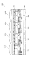
- FIG. 10 is a structural cross-sectional view of a conventional solid-state imaging device disclosed in Patent Document 1.
- the solid-state imaging device 900 disclosed in the figure includes a large number of pixels 902R, 902G, and 902B. Each pixel is formed in the semiconductor substrate 901 below the photoelectric conversion film 903 that absorbs light in a specific wavelength region formed above the semiconductor substrate 901 and generates a charge corresponding thereto.
- Patent Document 1 further discloses a digital camera including the solid-state imaging device 900 having the above-described configuration.
- exposure condition determining means for determining the exposure condition of the photoelectric conversion element 904 and a signal from the photoelectric conversion film 903 included in each pixel in imaging under the exposure condition do not appear to exceed the saturation level.
- an applied voltage adjusting means for adjusting a voltage applied to the photoelectric conversion film 903. Imaging based on the exposure conditions is performed in a state where the voltage adjusted by the applied voltage adjusting means is applied to the photoelectric conversion film 903.
- the present invention has been made in view of the above problems, and an object of the present invention is to provide an imaging apparatus capable of capturing a high-quality still image without a time lag during shooting, and a driving method thereof.
- an imaging device includes a photoelectric conversion unit that photoelectrically converts incident light into a signal charge, and a pixel that includes a reset unit that resets the charge accumulated in the photoelectric conversion unit.
- a solid-state imaging device arranged in a matrix on a substrate, a mechanical shutter for simultaneously performing light shielding and exposure for all the pixels, opening and closing of the mechanical shutter, application of voltage to the photoelectric conversion unit, And a timing control unit that controls the timing of resetting by the reset unit, and the timing control unit closes the mechanical shutter when switching from an image monitoring mode to a still image shooting mode.
- the charge accumulated in all the pixels is applied to the photoelectric conversion unit by applying a voltage to the photoelectric conversion unit so that the charge generated in the photoelectric conversion unit cannot move.
- the first exposure is performed, and the first exposure is terminated by applying a voltage to the photoelectric conversion unit so that the electric charge generated in the photoelectric conversion unit cannot move while the mechanical shutter is in an open state.
- the pixel signal is read from the pixel to acquire a first still image, and the charge accumulated in all the pixels is reset to the reset unit.
- (2) The photoelectric conversion is performed while the mechanical shutter remains open.
- the second exposure is performed by applying a voltage that enables movement of the charge generated in the unit to the photoelectric conversion unit, and the charge generated in the photoelectric conversion unit with the mechanical shutter open.
- a voltage that enables movement of the charge generated in the unit to the photoelectric conversion unit, and the charge generated in the photoelectric conversion unit with the mechanical shutter open.
- the mechanical shutter opening and closing and the voltage application to the photoelectric conversion unit are controlled in conjunction with each other, so that a plurality of mechanical shutter operations are not required. Therefore, when the physical time lag is reduced and a dynamic object is shot, blurring and distortion of the subject are reduced, and high-speed shooting can be realized. Furthermore, since the number of opening and closing of the mechanical shutter can be reduced, the physical life of the mechanical shutter is extended.
- the length of the first exposure period in which the first exposure is performed may be different from the length of the second exposure period in which the second exposure is performed.
- the timing control unit continuously captures n times while the mechanical shutter is in an open state, obtains n (n is a natural number of 2 or more) still images having different exposure periods, and the n The still images may be combined to generate m (m is a natural number, n ⁇ m) still images.
- a voltage value applied to the photoelectric conversion unit so that the charge generated in the photoelectric conversion unit can be moved, and when the second exposure is performed.
- the voltage value applied to the photoelectric conversion unit may be different from a voltage value that enables movement of charges generated in the photoelectric conversion unit.
- the timing control unit continuously captures n times while the mechanical shutter is in an open state, and the n (n is a natural number of 2 or more) different voltage values applied to the photoelectric conversion unit during exposure. Still images may be acquired and the n still images may be combined to generate m (m is a natural number, n ⁇ m) still images.
- the voltage value applied to the photoelectric conversion unit to enable movement of charges generated in the photoelectric conversion unit may be a value at which the black level of the video signal is output from the pixel as the pixel signal.
- the timing control unit may perform signal processing on an image other than the black level image on the basis of the black level image.
- the timing control unit performs a difference for each pixel between the black level image data and the reference image data provided from the outside, and a pixel whose difference value exceeds a certain value is determined as a defective pixel. Judgment may be made and a pixel at the same position as the defective pixel in the image other than the black level image may be corrected.
- the black level can be corrected by clamping the black level using the black level image with respect to the normal exposure image. Therefore, it is possible to provide a high-quality still image, and it is possible to make the effective pixel unit and the black level detection unit in the same position, so that the solid-state imaging device can be downsized and the black level can be corrected with high accuracy. realizable.
- the timing control unit further includes a focus lens and a memory for recording the pixel signal data, and the timing control unit further controls the focal length of the focus lens to continuously shoot a plurality of still images. , Acquiring the first still image and the second still image while changing the focal length of the focus lens, and storing the data of the first still image and the second still image in the memory It may be stored.
- the present invention can be realized not only as an imaging apparatus including such characteristic means, but also as a driving method of the imaging apparatus using the characteristic means included in the imaging apparatus as a step. .
- the mechanical shutter opening / closing and the voltage application to the photoelectric conversion unit are controlled in conjunction with each other, so that a plurality of mechanical shutter operations are not required. . Therefore, it is possible to realize high-accuracy high-speed shooting with reduced physical time lag and reduced blurring and distortion of the subject.
- FIG. 1 is a block configuration diagram of an imaging apparatus according to the first embodiment.
- FIG. 2 is a structural cross-sectional view of a unit cell of the solid-state imaging device according to the first embodiment.
- FIG. 3 is a drive timing chart in still image shooting of a general imaging apparatus.
- FIG. 4 is a drive timing chart in still image shooting of the imaging apparatus according to the first embodiment.
- FIG. 5 is a drive timing chart in still image shooting of the imaging apparatus according to the second embodiment.
- FIG. 6 is a drive timing chart in still image shooting of the imaging apparatus according to the third embodiment.
- FIG. 7A is a reference black level image diagram of the solid-state imaging device according to the third embodiment.
- FIG. 7B is a black level image diagram of the solid-state imaging device according to the third embodiment.
- FIG. 7A is a reference black level image diagram of the solid-state imaging device according to the third embodiment.
- FIG. 7B is a black level image diagram of the solid-state imaging device according to the third embodiment.
- FIG. 7C is a normal exposure image diagram of the solid-state imaging device according to the third embodiment.
- FIG. 7D is a corrected image diagram of the solid-state imaging device according to the third embodiment.
- FIG. 8 is a drive timing chart in still image shooting of the imaging apparatus according to the fourth embodiment.
- FIG. 9 is an image diagram of the solid-state imaging device according to the fourth embodiment.
- FIG. 10 is a structural cross-sectional view of a conventional solid-state imaging device disclosed in Patent Document 1. In FIG.
- FIG. 1 is a block diagram of the imaging apparatus according to the first embodiment.
- the imaging device 1 shown in the figure includes a solid-state imaging device 10, a signal processing unit 20, a mechanical shutter 30, a focus lens 40, and a memory 50.
- pixels having a photoelectric conversion unit that photoelectrically converts incident light into a signal charge and a reset unit that resets the charge accumulated in the photoelectric conversion unit are arranged in a matrix on the substrate.
- the light signal that has passed through the focus lens 40 and the mechanical shutter 30 becomes the image signal 11 in the solid-state imaging device 10, and is signal-processed by the signal processing unit 20 to output the video signal 21.
- a memory 50 is used for signal processing as needed.
- the signal processing unit 20 supplies and controls the photoelectric conversion film application voltage 22 applied to the photoelectric conversion film of the solid-state imaging device 10.
- the signal processing unit 20 controls a mechanical shutter control signal 23 for controlling the mechanical shutter 30 and a focus lens control signal 24 for controlling the focus lens 40 in conjunction with the photoelectric conversion film application voltage 22. That is, the signal processing unit 20 is a timing control unit that controls the opening / closing of the mechanical shutter 30, the voltage application to the photoelectric conversion unit, and the pixel reset timing. Details of the interlock control will be described later.
- FIG. 2 is a structural cross-sectional view of a unit cell of the solid-state imaging device according to the first embodiment.
- an amplification transistor, a selection transistor, and a reset transistor are formed on the semiconductor substrate 101.
- the amplification transistor includes a gate electrode 105, a diffusion layer 109 that is a drain, and a diffusion layer 110 that is a source.
- the selection transistor includes a gate electrode 106, a diffusion layer 110 that is a drain, and a diffusion layer 110 that is a source.
- the source of the amplification transistor and the drain of the selection transistor are a common diffusion layer 110.
- the reset transistor is a reset unit including a gate electrode 107, a diffusion layer 113 which is a drain, and a diffusion layer 112 which is a source.
- the diffusion layer 109 and the diffusion layer 112 are separated by the element isolation region 102.
- An insulating film 103 is formed on the semiconductor substrate 101 so as to cover each transistor.
- the photoelectric conversion unit includes a photoelectric conversion film 114 made of amorphous silicon or the like, a unit cell electrode 115 formed on the lower surface of the photoelectric conversion film 114, and a transparent electrode 108 formed on the upper surface of the photoelectric conversion film 114. Yes.
- the unit cell electrode 115 is connected to the gate electrode 105 of the amplification transistor and the diffusion layer 112 which is the source of the reset transistor via the contact 104.
- the diffusion layer 112 connected to the gate electrode 107 functions as a storage diode.
- pixels having a photoelectric conversion unit that photoelectrically converts incident light into a signal charge and a reset unit that resets the charge accumulated in the photoelectric conversion unit are arranged in a matrix on the substrate.
- the incident light is absorbed by the photoelectric conversion film 114, and carriers corresponding to the absorbed light amount are generated.
- the generated carriers are transferred to the diffusion layer 112 side and diffused. Accumulated in layer 112.
- FIG. 3 is a drive timing chart in still image shooting of a general imaging device.
- FIG. 4 is a drive timing chart when two still images are continuously shot by a general imaging device.
- the solid-state imaging device is all reset while the mechanical shutter is open (first reset period).
- a period until the mechanical shutter is closed by the mechanical shutter control signal 923 is the first exposure time, and the first image signal is read (first reading period).
- the second shutter exposure period is a period until the second mechanical shutter is closed by the mechanical shutter control signal 923 (second exposure period). Read (second read period).
- the mechanical shutter is necessary to determine the exposure time
- the first mechanical shutter operation is necessary for the first still image shooting
- the second mechanical image is 2 for the second still image shooting.
- a second mechanical shutter operation is required. That is, two mechanical shutter operations are required for continuous shooting of two still images.
- FIG. 4 is a drive timing chart in still image shooting of the imaging apparatus according to the first embodiment.
- a voltage at which carriers generated in the photoelectric conversion film 114 cannot move is V2
- a voltage at which carrier electrons or holes generated in the photoelectric conversion film 114 can move is V1.
- the solid-state imaging device 10 can obtain excellent characteristics with respect to reset noise and random noise by performing feedback reset in units of rows by setting the photoelectric conversion film application voltage 22 to V2.
- the mechanical shutter 30 is closed by the mechanical shutter control signal 23, and the photoelectric conversion film applied voltage 22 is set to V2 to execute feedback reset in units of rows. (First reset period).
- the all reset operation is completed in the solid-state imaging device 10. Reducing noise such as random noise with high accuracy by this all reset operation is very effective for improving the image quality at the time of photographing a plurality of images, which will be described later.
- the purpose of closing the mechanical shutter 30 in the present embodiment is not to determine the exposure time as in the general imaging device disclosed in FIG. 3, but the effect of suppressing the reset noise random noise of the solid-state imaging device 10. It is for improving.
- the photoelectric conversion film application voltage 22 is set to V1
- the mechanical shutter 30 is opened, and the first exposure is started.
- the period until the photoelectric conversion film application voltage 22 is set to V2 corresponds to the first exposure period.
- reading of the first sheet is performed with the photoelectric conversion film application voltage 22 set to V2 (first reading period).
- the photoelectric conversion film application voltage 22 set to V2 (first reading period).
- a feedback reset is performed in units of rows for the second image (second reset period).
- the photoelectric conversion film application voltage 22 is set to V1
- the mechanical shutter 30 is left open, and the second exposure is started. To do.
- the second exposure period until the photoelectric conversion film application voltage 22 is set to V2 is the second exposure time.
- the second sheet is read with the photoelectric conversion film applied voltage 22 set to V2 (second reading period).
- a feedback reset is executed in units of rows (third reset period).
- the mechanical shutter 30 is closed and the mechanical shutter 30 is opened after the reset is completed. Is preferable.
- the above-described interlocking control of the mechanical shutter 30 and the photoelectric conversion film applied voltage 22 enables continuous shooting of two still images with a single mechanical shutter operation.
- a driving example of two-shot continuous shooting has been described.
- it can be realized by one mechanical shutter operation.
- the signal processing unit 20 serving as the host of the solid-state imaging device 10 of the present embodiment controls the mechanical shutter control signal 23 and the photoelectric conversion film applied voltage 22 in conjunction with each other.
- the mechanical shutter 30 is opened, and the voltage V1 that enables movement of charges generated in the photoelectric conversion film 114 is transferred to the photoelectric conversion film. 114 is applied.
- the first exposure is executed.
- the voltage V2 that makes the electric charge generated in the photoelectric conversion film 114 immovable is applied to the photoelectric conversion film 114 while the mechanical shutter 30 remains open.
- the first exposure is completed, the pixel signal is read from the pixel, and the first still image is acquired.
- the charge accumulated in all the pixels is reset by the reset unit.
- the voltage V1 is applied to the photoelectric conversion film 114 while the mechanical shutter 30 remains open.
- the second exposure is executed.
- the voltage V2 is applied to the photoelectric conversion film 114 while the mechanical shutter 30 remains open.
- the second exposure is completed, the pixel signal from the pixel is read, and the second still image is acquired.
- the signal processing unit 20 displays the mechanical shutter control signal 23 and the photoelectric conversion film applied voltage 22 with the drive timing chart shown in FIG. Interlocking control is performed as follows. As a result, random noise peculiar to the solid-state imaging device can be reduced, and a plurality of still images can be captured by one mechanical shutter operation.
- the number of still images continuously shot can be freely set by instructing the signal processing unit 20 from an external photographer.
- the image pickup apparatus and the solid-state image pickup apparatus do not require a plurality of mechanical shutter operations by interlockingly controlling the voltage control applied to the mechanical shutter and the photoelectric conversion film.
- a physical object is shot with a reduced physical time lag, blurring and distortion of the subject are reduced, and high-speed shooting can be realized.
- the number of opening and closing of the mechanical shutter can be reduced, the physical life of the mechanical shutter is extended.
- the case where a high dynamic range is required for a still image is, for example, a case where the inside of the room and the outside of the window are simultaneously shot from inside the room. If you shoot in a dark room with the same amount of exposure, the exposure outside the bright window will be overexposed. On the other hand, when shooting with the exposure adjusted outside the bright window, the dark room may be dark and not visible.
- two still images are shot by setting different exposure times for the first and second shots.
- the first exposure time is set to be long and the first picture is taken with an exposure amount adjusted in a dark room.
- the second exposure time is set short and the second image is taken with an exposure amount adjusted outside the bright window.
- Two shot images are combined in the solid-state imaging device or the imaging device to generate one image having a high dynamic range.
- an image can be synthesized by the signal processing unit 20 using the memory 50, but the signal processing function and the memory function are mounted in the solid-state imaging device 10. If so, the images may be combined in the solid-state imaging device 10.
- the exposure time for the first and second image capturing is controlled by the signal processing unit 20 using the photoelectric conversion film applied voltage 22.
- a mechanical time lag is not required by linking the control of the photoelectric conversion film applied voltage and the mechanical shutter opening and closing, so that a plurality of mechanical shutter operations are not required. Reduce. In addition, when a dynamic object is photographed, blurring and distortion of the subject are reduced during image composition.
- two or more images with different exposure times have been described in a simple manner.
- two or more still images with different exposure times are taken and image synthesis is performed. It is preferable to do.
- two or more images can be physically captured by one mechanical shutter operation. That is, the signal processing unit 20 continuously captures n times while the mechanical shutter 30 is in the open state, acquires n (n is a natural number of 2 or more) still images having different exposure periods, and the n images.
- the still images may be combined to generate m (m is a natural number, n ⁇ m) still images.
- the first exposure period and the second exposure period are arranged in the order of the first exposure period having a long exposure time and the second exposure period having a short exposure time, but the order of the long and short exposure times is reversed. It doesn't matter.
- the imaging device and the solid-state imaging device of the present embodiment a plurality of still images with different exposure times can be taken, and the order can be freely set regardless of the length of the exposure time.
- the purpose of closing the mechanical shutter 30 in the first reset period is not to determine the exposure time as in the conventional solid-state imaging device but to improve the effect of suppressing the reset noise random noise of the solid-state imaging device 10. This is to make it happen. From this point of view, there are cases where it is better to process a frame with a small exposure amount in which reset noise and random noise become more prominent.
- the signal processing unit 20 controls the mechanical shutter control signal 23 and the photoelectric conversion film applied voltage 22 in conjunction with each other as shown in the drive timing chart of FIG.
- random noise peculiar to the solid-state imaging device can be reduced, and still image shooting with different exposure times can be performed by one mechanical shutter operation.
- the effect of the present invention cannot be realized with a simple combination of a mechanical shutter and a solid-state imaging device. Further, the number of still images continuously shot and each exposure time can be freely set by instructing the signal processing unit 20 from an external photographer.
- the exposure time difference may be the amount of movement of the object.
- a single mechanical shutter operation is performed for shooting a plurality of images with different exposure amounts in a state where the exposure time is uniform by interlocking control of the mechanical shutter opening and closing and the photoelectric conversion film applied voltage. Realize with.
- FIG. 5 is a drive timing chart in still image shooting of the imaging apparatus according to the second embodiment.
- the drive that can basically shoot a plurality of still images by one mechanical shutter operation is the same as the first embodiment.
- the difference is that the photoelectric conversion film applied voltage 22 is different between the first and second images.
- the photoelectric conversion film application voltage 22 in the first exposure period and the second exposure period is changed in accordance with the exposure amount.
- the exposure amount conversion efficiency of the first image shooting and the second image shooting is determined by the signal processing unit 20 using the photoelectric conversion film applied voltage 22 in accordance with each exposure amount.
- the solid-state imaging device can control the amount of carrier movement and the conversion efficiency by changing the voltage value of the photoelectric conversion film application voltage 22. By controlling this conversion efficiency, it is possible to control as if the exposure amount was changed without changing the exposure time.
- the inside of the room and the outside of the window are shot simultaneously. If you shoot in a dark room with the same amount of exposure, the exposure outside the bright window will be overexposed. On the other hand, when shooting with the exposure adjusted outside the bright window, the dark room may be dark and not visible.
- the photoelectric conversion film applied voltage 22 is set to a voltage value V1 in a state where the conversion efficiency is high and photographed with an exposure amount adjusted in a dark room, and set to a voltage value V3 in a state where the conversion efficiency is low. Then, shoot with the exposure amount adjusted to the outside of the bright window. Two shot images are combined in the solid-state imaging device or the imaging device to generate one image having a high dynamic range.
- the mechanical shutter operation is not required multiple times by interlocking the control of the photoelectric conversion film applied voltage and the mechanical shutter operation, and physical Time lag is reduced.
- a dynamic object is photographed, blurring and distortion of the subject are reduced.
- dynamic blur may cause coloration in a contour portion or the like more prominently.
- the imaging apparatus according to the present embodiment since high-speed shooting is possible, high image quality can be ensured compared to the conventional configuration. Furthermore, since the mechanical shutter can be opened and closed only once, image blurring due to opening and closing of the mechanical shutter can be reduced.
- two or more photoelectric conversion films have different conversion efficiencies. It is preferable to shoot a still image and synthesize the image. It is obvious that even in the configuration of the second embodiment, two or more images can be physically captured by one mechanical shutter operation. That is, the signal processing unit 20 may perform continuous shooting n times while the mechanical shutter 30 is in the open state. Specifically, n (n is a natural number greater than or equal to 2) still images having different voltage values applied to the photoelectric conversion film 114 during the exposure of the n consecutive photographings are acquired, and the n still images are acquired. May be combined to generate m (m is a natural number, n ⁇ m) still images.
- the first exposure period in which the conversion efficiency of the photoelectric conversion film is high and the second exposure period in which the conversion efficiency of the photoelectric conversion film is low are in order.
- the order of the conversion efficiency may be reversed. According to the imaging apparatus and the solid-state imaging apparatus of the present embodiment, it is possible to capture a plurality of still images with different exposure amount conversion coefficients, and the order can be freely set regardless of the level of the conversion efficiency.
- the purpose of closing the mechanical shutter 30 in the first reset period is not to determine the exposure time as in the conventional solid-state imaging device but to improve the effect of suppressing the reset noise random noise of the solid-state imaging device 10. This is to make it happen. From this point of view, there are cases where it is better to process the frame with low conversion efficiency, in which reset noise and random noise become more prominent.
- the signal processing unit 20 controls the mechanical shutter control signal 23 and the photoelectric conversion film applied voltage 22 in conjunction with each other as shown in the drive timing chart of FIG.
- the effect of the present invention cannot be realized with a simple combination of a mechanical shutter and a solid-state imaging device.
- the number of still images continuously shot and each exposure amount conversion coefficient can be freely set by instructing the signal processing unit 20 from an external photographer.
- the mechanical shutter 30 and the photoelectric conversion film application voltage 22 are interlocked to control the photoelectric conversion film application voltage 22 with the exposure time uniform.
- the mechanical shutter 30 and the photoelectric conversion film application voltage 22 are interlocked to control the photoelectric conversion film application voltage 22 with the exposure time uniform.
- a minute dark current is generated in the photodiode (photoelectric conversion film) of the solid-state imaging device even in the dark when the photoelectric conversion is not structurally performed. Deterioration of image quality is inevitable unless the video signal is corrected and clamped to an appropriate black level due to the generation of dark current.
- an OB (Optical Black) area that is optically shielded and generates a dark current in the same way as a normal pixel portion in order to detect and remove dark current and adjust the black level of the video signal. The dark current value is detected. The black level of the video signal is corrected and clamped by subtracting this dark current value from the output of the effective pixel unit used in the actual video.
- the dark current level is detected by integrating and averaging the output values of the OB region in order to reduce the variation, the dark current measurement accuracy deteriorates if the area of the OB region is small. From this point of view, narrowing the OB region leads to image quality degradation, but the solid-state imaging device is also required to be miniaturized in order to develop a small camera that has a strong market demand. Therefore, the chip area of the OB region in the solid-state imaging device is also an issue.
- the generation of dark current has temperature dependence, and an error may occur in the dark current value due to gain multiplication for image enhancement. For this reason, in the signal processing in which the dark current value measured in the past in the past or a predetermined constant value as the dark current level is subtracted from the output of the effective pixel unit used in the actual image, an error occurs in the correction value. It leads to deterioration of the image.
- the OB area and the effective pixel area are physically different areas. For this reason, if the effective pixel area becomes large, even if there is a slight difference in the structure of the chip layout design or manufacturing process variations, it is not possible to correct the black level properly, and the black image can be corrected within the same screen. There also arises a problem of generation of so-called luminance shading that causes uneven levels.
- the solid-state imaging device and the imaging device according to the present embodiment also solve the above problems. Details will be described below.
- FIG. 6 is a drive timing chart in still image shooting of the imaging apparatus according to the third embodiment.
- the mechanical shutter 30 and the photoelectric conversion film applied voltage 22 are interlocked and controlled in a state where the exposure time is uniform, thereby realizing shooting of a plurality of sheets having different conversion efficiency of the photoelectric conversion film by one mechanical shutter operation.
- the driving that enables photographing of a plurality of still images with a single mechanical shutter operation is the same as in the first and second embodiments. The difference is the photoelectric conversion film applied voltage 22 at the time of photographing the first image and at the time of photographing the second image.
- the photoelectric conversion film application voltage 22 in the black level period is set to a voltage value V4 at which the black level can be output
- the photoelectric conversion film application voltage 22 in the normal exposure period is set to a voltage value V1 at which normal exposure is possible. It is. That is, V4 is a value at which the black level of the video signal is output from the pixel as an image signal.
- the solid-state imaging device can control the conversion efficiency by changing the voltage value of the photoelectric conversion film application voltage 22 as in the second embodiment.
- the exposure time is constant, and control can be performed as if the exposure amount was changed.
- the photoelectric conversion film is shielded from light by the electrode, and further, the conversion efficiency can be controlled by controlling the amount of carrier movement by controlling the voltage applied to the photoelectric conversion film. Is possible. Therefore, it is possible to output the black level of the video signal even if it is not optically shielded unlike a general solid-state imaging device (for example, an OB region of a CCD image sensor).
- FIG. 7A is a reference black level image diagram of the solid-state imaging device according to the third embodiment.
- FIG. 7B is a black level image diagram of the solid-state imaging device according to the third embodiment.
- FIG. 7C is a normal exposure image diagram of the solid-state imaging device according to the third embodiment.
- FIG. 7D is a corrected image diagram of the solid-state imaging device according to the third embodiment.
- the black level image 202 in FIG. 7B is an image output when the photoelectric conversion film application voltage 22 in FIG. 6 is set to V4.
- Data of the reference black level image 201 is owned in advance in the solid-state imaging device or the imaging device for each pixel, and the data of the reference black level image 201 is subtracted for each pixel from the data of the black level image 202.
- the scratch 212 can be detected.
- the scratch correction 214 can be performed as in the corrected image 204 shown in FIG. 7D.
- the address of the scratch position is normally detected in a dark light-shielding state during set shipment inspection at the factory, and the pixel of the scratch address is corrected as a real product during normal operation. .
- scratches may be generated by dust floating in the package, and it is impossible to correct the scratches due to the movement of the dust.
- the signal processing unit 20 performs signal processing on an image other than the black level image 202 on the basis of the black level image 202.
- the defect correction is applied only to the pixel where the defect is detected by subtracting the data of the reference black level image 201 from the data of the black level image 202 for each pixel as in the present embodiment. It is possible to suppress degradation of resolution. Thereby, the resolution of the whole screen is not deteriorated. That is, the signal processing unit 20 compares the data of the black level image 202 and the data of the normal exposure image 203 for each pixel, determines a pixel whose difference value exceeds a certain value as a defective pixel, and performs normal exposure. In the image 203, the pixel at the same position as the defective pixel is scratch-corrected to obtain a corrected image 204.
- the voltage level of the photoelectric conversion film application voltage 22 is adjusted in accordance with the exposure amount of the subject, thereby controlling the conversion efficiency and executing normal exposure photography.
- the time lag from the black level period to the normal exposure period is a very short time in total of the first reading period and the second reset period for reading the black level image data, and a high-speed moving object is photographed. This is a time difference that does not cause any problems.
- the OB clamp of a general solid-state imaging device there is an OB area that is shielded from light other than the effective pixel portion, and there is a method in which the entire effective pixel portion is OB clamped using a value obtained by averaging the output values. .
- the OB area is present in the horizontal direction of the effective pixel portion, there is a method of performing OB clamping using a value obtained by averaging in line line units.
- an OB area is physically required separately, and reducing the OB area leads to deterioration in the accuracy of the OB clamp, so that it is difficult to reduce the size of the solid-state imaging device.
- the solid-state imaging device can use a pixel at the same position as the effective pixel unit as an OB pixel, it is not necessary to secure a separately shielded OB region. Miniaturization can be realized.
- the solid-state imaging device uses pixels at the same position as the OB clamp. Accordingly, it is possible to reduce a clamping error when there is a process variation in chip layout design and manufacturing that occurs when a physically different region is used as the OB clamp region. Disturbances in black balance cause a bias in luminance and become a problem called luminance shading. However, the configuration of this embodiment has an effect of suppressing this luminance shading.
- the signal processing unit 20 controls the mechanical shutter control signal 23 and the photoelectric conversion film applied voltage 22 in conjunction with each other as shown in the drive timing chart of FIG.
- random noise can be reduced, and a plurality of different still images can be captured by one mechanical shutter operation.
- scratch detection and black level correction clamping can be performed in the same pixel unit.
- the effect of the present invention cannot be realized with a simple combination of a mechanical shutter and a solid-state imaging device.
- the number of still images continuously shot, the detection of scratches and the ON / OFF of the scratch correction, and the ON / OFF of the black level correction can be freely set by instructing the signal processing unit 20 from an external photographer.
- two still images of the black level image 202 and the normal exposure image 203 can be photographed by one mechanical shutter operation by interlocking control of the mechanical shutter 30 and the photoelectric conversion film applied voltage 22. Then, by subtracting the data of the existing reference black level image 201 from the data of the black level image 202 in units of pixels, the scratch 212 can be detected in real time, and the scratch correction 214 can be performed. Further, the black level can be corrected by clamping the black level to the normal exposure image 203 using the black level image 202. Therefore, it is possible to provide a high-quality still image, and it is possible to make the effective pixel unit and the black level detection unit in the same position, so that the solid-state imaging device can be downsized and the black level can be corrected with high accuracy. realizable.
- the solid-state imaging device and the imaging device according to the present embodiment also solve the above-described problems, and it is possible to shoot a plurality of still images by one mechanical shutter operation, and further use this to obtain an appropriate black level.
- the purpose is to realize the correction. In addition, it provides a still image with optimum focus. Details will be described below.
- the interlocking of the mechanical shutter 30 and the photoelectric conversion film applied voltage is controlled by the solid-state imaging device and imaging device according to the present embodiment.
- a single mechanical shutter operation enables high-speed continuous shooting of a plurality of images while moving the focus lens 40 from the tele (near distance) side to the wide (far distance) side or vice versa. Therefore, it is possible to select an image having the optimum focus after shooting.
- FIG. 8 is a drive timing chart in still image shooting of the imaging apparatus according to the fourth embodiment.
- FIG. 9 is an image diagram of the solid-state imaging device according to the third embodiment.
- the focus lens 40 shown in FIG. 1 is controlled by the signal processing unit 20.
- the signal processing unit 20 closes the mechanical shutter 30 and performs a reset (first reset period). Thereafter, the mechanical shutter 30 is opened, and the focus lens 40 is moved from the optimum state for photographing near the tele side to the optimum state for photographing on the far side of the wide side.
- An image signal (wide exposure period) by side photographing can be obtained.
- These image signals are stored in the memory 50. That is, when continuously shooting a plurality of still images, the signal processing unit 20 is exposed in the first still image exposed in the tele exposure period and the wide exposure period while changing the focal length of the focus lens 40. The second still image is acquired.
- the still image data is stored in the memory 50.
- FIG. 8 shows the case where two still images are acquired, there is no limit to the number of shots.
- FIG. 9 shows an image diagram when four still images are acquired. In the figure, images taken in the order of the tele-side image 301 to the wide-side image 304 are drawn. In the tele-side images 301 and 302, the subject 90 is shown large, but the focus is not in focus. On the other hand, the wide side image 304 shows the subject 90 in a small size, and it can be seen that the wide side image 303 is the optimum still image. The photographer can extract the wide-side image 303 from the four types of still images stored in the solid-state imaging device according to this embodiment or the memory 50 in the imaging device.
- the focus lens 40 is operated from the tele-side image 301 to the wide-side image 304.
- the wide-side image 304 and the tele-side image 301 may be operated in this order.
- the signal processing unit 20 determines the mechanical shutter control signal 23, the photoelectric conversion film applied voltage 22, and the position of the focus lens 40 according to the drive timing in FIG. Interlocking control is performed like a chart.
- random noise peculiar to the solid-state imaging device can be reduced, and a plurality of different still images can be captured by one mechanical shutter operation, and a plurality of still images with different focus focal positions can be captured. Therefore, by taking a picture while moving the focus lens and recording each image in the memory, it is possible to select a still picture having an optimum focus focus after the photography.
- the effect of the present invention cannot be realized with a simple combination of a mechanical shutter and a solid-state imaging device. Further, the number of still images continuously shot and the AF (autofocus) function can be freely set by instructing the signal processing unit 20 from an external photographer.
- the imaging device and its driving method of this indication were explained based on an embodiment, the imaging device and its driving method concerning the present invention are not limited to the above-mentioned embodiment.
- the length of the first exposure period and the length of the second exposure period may be the same.
- the voltage value of the photoelectric conversion film applied voltage in the first exposure period and the second exposure period may be the same. Even in these cases, a plurality of still images, that is, continuous shooting can be performed by one mechanical shutter operation.
- an imaging device capable of capturing a plurality of still images with a single mechanical shutter operation can be realized, and is particularly effective for a video camera, a digital still camera, and a camera module for mobile devices such as a mobile phone.
- Solid-state imaging device 11 Image signal 20 Signal processing part 21 Video signal 22 Photoelectric conversion film application voltage 23,923 Mechanical shutter control signal 24 Focus lens control signal 25 Reset pulse 30 Mechanical shutter 40 Focus lens 50 Memory 90 Subject 101 Semiconductor substrate 102 Element isolation region 103 Insulating film 104 Contact 105, 106, 107 Gate electrode 108 Transparent electrode 109, 110, 111, 112, 113 Diffusion layer 114, 903 Photoelectric conversion film 115 Unit cell electrode 201 Reference black level image 202 Black level image 203 Normal Exposure image 204 Correction image 212 Scratch 214 Scratch correction 900 Solid-state imaging device 901 Semiconductor substrate 902B, 902G, 902R Pixel 904 Photoelectric conversion device 924 C CD all reset signal
Abstract
This imaging device (1) is equipped with a solid-state imaging unit (10) wherein pixels are arranged in a matrix, a mechanical shutter (30), and a signal processing unit (20). The signal processing unit (20) resets electric charges accumulated in all the pixels by bringing the mechanical shutter (30) into a closed state and applying voltage (V2) to a photoelectric conversion unit, executes a first exposure by bringing the mechanical shutter (30) into an open state and applying voltage (V1) to the photoelectric conversion unit, ends the first exposure by applying voltage (V2) to the photoelectric conversion unit with the mechanical shutter (30) being in the open state, obtains a first still image by reading pixel signals, resets all the pixels, executes a second exposure by applying voltage (V1) to the photoelectric conversion unit with the mechanical shutter (30) being in the open state, ends the second exposure by applying voltage (V2) to the photoelectric conversion unit with the mechanical shutter (30) being in the open state, and obtains a second still image by reading pixel signals.
Description
本発明は、撮像装置及びその駆動方法に関する。
The present invention relates to an imaging apparatus and a driving method thereof.
イメージセンサなどの固体撮像装置を用いたデジタルカメラで静止画を撮影する場合には、露光量を調整するためにメカシャッタが必要であり、固体撮像装置の画素部をオールリセットした後、メカシャッタを閉じるまでが露光時間となる。
When taking a still image with a digital camera using a solid-state imaging device such as an image sensor, a mechanical shutter is required to adjust the exposure amount. After the pixel portion of the solid-state imaging device is all reset, the mechanical shutter is closed. Up to the exposure time.
図10は、特許文献1に開示された従来の固体撮像素子の構造断面図である。同図に開示された固体撮像素子900は、多数の画素902R、902G及び902Bを有する。各画素は、半導体基板901上方に形成された特定の波長域の光を吸収してこれに応じた電荷を発生する光電変換膜903と、光電変換膜903下方の半導体基板901内に形成された光電変換素子904とを含む。特許文献1には、さらに、上記構成の固体撮像素子900を備えるデジタルカメラが開示されている。上記デジタルカメラは、光電変換素子904の露光条件を決定する露光条件決定手段と、当該露光条件での撮像において各画素に含まれる光電変換膜903からの信号に飽和レベルを超えるものが存在しないように、光電変換膜903に印加する電圧を調整する印加電圧調整手段とを備える。印加電圧調整手段で調整された電圧が光電変換膜903に印加された状態で、上記露光条件に基づいた撮像が行われる。
FIG. 10 is a structural cross-sectional view of a conventional solid-state imaging device disclosed in Patent Document 1. The solid-state imaging device 900 disclosed in the figure includes a large number of pixels 902R, 902G, and 902B. Each pixel is formed in the semiconductor substrate 901 below the photoelectric conversion film 903 that absorbs light in a specific wavelength region formed above the semiconductor substrate 901 and generates a charge corresponding thereto. A photoelectric conversion element 904. Patent Document 1 further discloses a digital camera including the solid-state imaging device 900 having the above-described configuration. In the digital camera, exposure condition determining means for determining the exposure condition of the photoelectric conversion element 904 and a signal from the photoelectric conversion film 903 included in each pixel in imaging under the exposure condition do not appear to exceed the saturation level. And an applied voltage adjusting means for adjusting a voltage applied to the photoelectric conversion film 903. Imaging based on the exposure conditions is performed in a state where the voltage adjusted by the applied voltage adjusting means is applied to the photoelectric conversion film 903.
しかしながら、特許文献1に開示された従来の固体撮像素子にメカシャッタを組み合わせると、1回の撮像動作に対して複数回のメカシャッタ動作が必要であり、物理的なタイムラグが発生する。この状態で動的な物体を撮影した場合は、被写体のブレや歪みが発生し、高速撮影を実現できないという課題を有する。
However, when a mechanical shutter is combined with the conventional solid-state imaging device disclosed in Patent Document 1, a plurality of mechanical shutter operations are required for one imaging operation, and a physical time lag occurs. When a dynamic object is photographed in this state, there is a problem that blurring and distortion of the subject occur and high-speed photographing cannot be realized.
本発明は、上記課題に鑑みてなされたものであり、撮影時のタイムラグがない高画質な静止画像を撮像できる撮像装置及びその駆動方法を提供することを目的とする。
The present invention has been made in view of the above problems, and an object of the present invention is to provide an imaging apparatus capable of capturing a high-quality still image without a time lag during shooting, and a driving method thereof.
上記課題を解決するために、本発明の一態様に係る撮像装置は、入射光を信号電荷に光電変換する光電変換部と前記光電変換部に蓄積された電荷をリセットするリセット部とを有する画素が基板上に行列状に配置された固体撮像装置と、全ての前記画素に対して、一斉に遮光及び露光を行わせるためのメカシャッタと、前記メカシャッタの開閉、前記光電変換部への電圧印加、及び、前記リセット部によるリセットのタイミングを制御するタイミング制御部とを備え、前記タイミング制御部は、画像をモニタするモードから静止画を撮影するモードへと切り替える場合には、前記メカシャッタを閉状態にして、前記光電変換部で発生した電荷を移動不可とする電圧を前記光電変換部に印加することにより、全ての前記画素に蓄積された電荷をリセットし、複数の静止画を連続撮影する場合には、(1)前記メカシャッタを開状態にして、前記光電変換部で発生した電荷を移動可能とする電圧を前記光電変換部に印加することにより第1の露光を実行し、前記メカシャッタが開状態のままで、前記光電変換部で発生した電荷を移動不可とする電圧を前記光電変換部に印加することにより、前記第1の露光を終了し前記画素から画素信号を読み出して第1の静止画を取得するとともに、全ての前記画素に蓄積された電荷を前記リセット部にリセットさせ、(2)前記メカシャッタが開状態のままで、前記光電変換部で発生した電荷を移動可能とする電圧を前記光電変換部に印加することにより第2の露光を実行し、前記メカシャッタが開状態のままで、前記光電変換部で発生した電荷を移動不可とする電圧を前記光電変換部に印加することにより、前記第2の露光を終了し前記画素からの画素信号を読み出して第2の静止画を取得することを特徴とする。
In order to solve the above problems, an imaging device according to one embodiment of the present invention includes a photoelectric conversion unit that photoelectrically converts incident light into a signal charge, and a pixel that includes a reset unit that resets the charge accumulated in the photoelectric conversion unit. A solid-state imaging device arranged in a matrix on a substrate, a mechanical shutter for simultaneously performing light shielding and exposure for all the pixels, opening and closing of the mechanical shutter, application of voltage to the photoelectric conversion unit, And a timing control unit that controls the timing of resetting by the reset unit, and the timing control unit closes the mechanical shutter when switching from an image monitoring mode to a still image shooting mode. The charge accumulated in all the pixels is applied to the photoelectric conversion unit by applying a voltage to the photoelectric conversion unit so that the charge generated in the photoelectric conversion unit cannot move. In the case of resetting and continuously shooting a plurality of still images, (1) by opening the mechanical shutter and applying a voltage to the photoelectric conversion unit that enables movement of charges generated in the photoelectric conversion unit. The first exposure is performed, and the first exposure is terminated by applying a voltage to the photoelectric conversion unit so that the electric charge generated in the photoelectric conversion unit cannot move while the mechanical shutter is in an open state. The pixel signal is read from the pixel to acquire a first still image, and the charge accumulated in all the pixels is reset to the reset unit. (2) The photoelectric conversion is performed while the mechanical shutter remains open. The second exposure is performed by applying a voltage that enables movement of the charge generated in the unit to the photoelectric conversion unit, and the charge generated in the photoelectric conversion unit with the mechanical shutter open. By applying a voltage to unmovable in the photoelectric conversion unit, and acquires the second still image and terminating the second exposure read out pixel signals from the pixels.
この構成によれば、静止画連写をするにあたり、メカシャッタ開閉と光電変換部への電圧印加とが連動制御されることにより、複数回のメカシャッタ動作が不要となる。よって、物理的なタイムラグが軽減し、動的な物体を撮影した場合は、被写体のブレや歪みが軽減し、高速撮影を実現できる。さらに、また、メカシャッタの開閉回数が軽減できるので、メカシャッタの物理的な寿命が延びる。
According to this configuration, when performing continuous shooting of still images, the mechanical shutter opening and closing and the voltage application to the photoelectric conversion unit are controlled in conjunction with each other, so that a plurality of mechanical shutter operations are not required. Therefore, when the physical time lag is reduced and a dynamic object is shot, blurring and distortion of the subject are reduced, and high-speed shooting can be realized. Furthermore, since the number of opening and closing of the mechanical shutter can be reduced, the physical life of the mechanical shutter is extended.
また、前記第1の露光が実行される第1露光期間の長さと前記第2の露光が実行される第2露光期間の長さとは異なってもよい。
In addition, the length of the first exposure period in which the first exposure is performed may be different from the length of the second exposure period in which the second exposure is performed.
また、前記タイミング制御部は、前記メカシャッタが開状態のままでn回連続撮影し、露光期間の長さがそれぞれ異なるn(nは2以上の自然数)枚の前記静止画を取得し、当該n枚の静止画を画像合成して、m(mは自然数でn≧m)枚の静止画を生成してもよい。
Further, the timing control unit continuously captures n times while the mechanical shutter is in an open state, obtains n (n is a natural number of 2 or more) still images having different exposure periods, and the n The still images may be combined to generate m (m is a natural number, n ≧ m) still images.
これにより、露光時間の異なる2枚以上の画像データを合成して、明るい所から暗い所までを表現できる高ダイナミックレンジの画像を作り出すことができる。
This makes it possible to create an image with a high dynamic range that can express from a bright place to a dark place by combining two or more pieces of image data with different exposure times.
また、前記第1の露光が実行される場合に前記光電変換部に印加される、前記光電変換部で発生した電荷を移動可能とする電圧値と、前記第2の露光が実行される場合に前記光電変換部に印加される、前記光電変換部で発生した電荷を移動可能とする電圧値とは異なってもよい。
In addition, when the first exposure is performed, a voltage value applied to the photoelectric conversion unit so that the charge generated in the photoelectric conversion unit can be moved, and when the second exposure is performed. The voltage value applied to the photoelectric conversion unit may be different from a voltage value that enables movement of charges generated in the photoelectric conversion unit.
また、前記タイミング制御部は、前記メカシャッタが開状態のままでn回連続撮影し、露光中に前記光電変換部に印加される電圧値がそれぞれ異なるn(nは2以上の自然数)枚の前記静止画を取得し、当該n枚の静止画を画像合成して、m(mは自然数でn≧m)枚の静止画を生成してもよい。
Further, the timing control unit continuously captures n times while the mechanical shutter is in an open state, and the n (n is a natural number of 2 or more) different voltage values applied to the photoelectric conversion unit during exposure. Still images may be acquired and the n still images may be combined to generate m (m is a natural number, n ≧ m) still images.
これにより、露光時間制御の不均一性が発生しない状態で、複数枚の静止画像を撮影することが可能となる。よって、これらの静止画像を合成することにより、高ダイナミックレンジな静止画像の生成が可能となる。
This makes it possible to shoot a plurality of still images in a state where non-uniformity in exposure time control does not occur. Therefore, by combining these still images, it is possible to generate a still image with a high dynamic range.
また、前記第1の露光が実行される場合に前記光電変換部に印加される、前記光電変換部で発生した電荷を移動可能とする電圧値、または、前記第2の露光が実行される場合に前記光電変換部に印加される、前記光電変換部で発生した電荷を移動可能とする電圧値は、前記画素から映像信号の黒レベルが前記画素信号として出力される値であってもよい。
In addition, when the first exposure is performed, a voltage value that is applied to the photoelectric conversion unit so that the charge generated in the photoelectric conversion unit can be moved, or when the second exposure is performed. The voltage value applied to the photoelectric conversion unit to enable movement of charges generated in the photoelectric conversion unit may be a value at which the black level of the video signal is output from the pixel as the pixel signal.
また、前記タイミング制御部は、前記黒レベルの画像を基準に、当該黒レベルの画像以外の画像を信号処理してもよい。
The timing control unit may perform signal processing on an image other than the black level image on the basis of the black level image.
また、前記タイミング制御部は、前記黒レベルの画像のデータと外部から提供される基準画像のデータとを前記画素ごとを差分し、当該差分の値が一定値を超えている画素を欠陥画素と判断し、前記黒レベルの画像以外の画像において前記欠陥画素と同位置の画素をキズ補正してもよい。
In addition, the timing control unit performs a difference for each pixel between the black level image data and the reference image data provided from the outside, and a pixel whose difference value exceeds a certain value is determined as a defective pixel. Judgment may be made and a pixel at the same position as the defective pixel in the image other than the black level image may be corrected.
これにより、通常露光画像に対して黒レベル画像を用いて黒レベルをクランプすることにより、黒レベル補正が可能となる。よって、高画質な静止画の提供が可能となると共に、有効画素部と黒レベル検出部とを同位置にすることが可能となるので、固体撮像装置の小型化及び高精度な黒レベル補正を実現できる。
Thus, the black level can be corrected by clamping the black level using the black level image with respect to the normal exposure image. Therefore, it is possible to provide a high-quality still image, and it is possible to make the effective pixel unit and the black level detection unit in the same position, so that the solid-state imaging device can be downsized and the black level can be corrected with high accuracy. realizable.
また、さらに、フォーカスレンズと、前記画素信号のデータを記録するメモリとを備え、前記タイミング制御部は、さらに、前記フォーカスレンズの焦点距離を制御し、複数の静止画を連続撮影する場合には、前記フォーカスレンズの前記焦点距離を変化させながら、前記第1の静止画及び前記第2の静止画を取得して、前記第1の静止画及び前記第2の静止画のデータを前記メモリに格納してもよい。
The timing control unit further includes a focus lens and a memory for recording the pixel signal data, and the timing control unit further controls the focal length of the focus lens to continuously shoot a plurality of still images. , Acquiring the first still image and the second still image while changing the focal length of the focus lens, and storing the data of the first still image and the second still image in the memory It may be stored.
これにより、フォーカスレンズを動かしながら、1回のメカシャッタ動作で複数枚の異なる静止画撮影が可能となる。つまり、フォーカス焦点位置が異なる複数枚の静止画撮影が可能となる。よって、これらの静止画撮影をメモリに記録することにより、最適なフォーカス焦点になっている静止画像を、撮影後に選択することが可能となる。
This makes it possible to shoot a plurality of different still images with a single mechanical shutter operation while moving the focus lens. That is, it is possible to shoot a plurality of still images with different focus focal positions. Therefore, by recording these still image shots in the memory, it is possible to select a still image having the optimum focus focus after the shooting.
なお、本発明は、このような特徴的な手段を備える撮像装置として実現することができるだけでなく、撮像装置に含まれる特徴的な手段をステップとする撮像装置の駆動方法として実現することができる。
The present invention can be realized not only as an imaging apparatus including such characteristic means, but also as a driving method of the imaging apparatus using the characteristic means included in the imaging apparatus as a step. .
本発明に係る撮像装置及びその駆動方法によれば、静止画連写をするにあたり、メカシャッタ開閉と光電変換部への電圧印加とが連動制御されることにより、複数回のメカシャッタ動作が不要となる。よって、物理的なタイムラグが軽減し、被写体のブレや歪みが軽減された高精度な高速撮影を実現できる。
According to the imaging apparatus and the driving method thereof according to the present invention, when performing continuous shooting of still images, the mechanical shutter opening / closing and the voltage application to the photoelectric conversion unit are controlled in conjunction with each other, so that a plurality of mechanical shutter operations are not required. . Therefore, it is possible to realize high-accuracy high-speed shooting with reduced physical time lag and reduced blurring and distortion of the subject.
以下、図面を参照しながら、各実施形態に係る固体撮像装置、撮像装置について説明する。なお、本発明について、以下の実施形態及び添付の図面を用いて説明を行うが、これは例示を目的としており、本発明がこれらに限定されることを意図しない。
Hereinafter, a solid-state imaging device and an imaging device according to each embodiment will be described with reference to the drawings. In addition, although this invention is demonstrated using the following embodiment and attached drawing, this is for the purpose of illustration and this invention is not intended to be limited to these.
(第1の実施形態)
まず、図1を用いて、本発明の第1の実施形態に係る撮像装置の構成を説明する。 (First embodiment)
First, the configuration of the imaging apparatus according to the first embodiment of the present invention will be described with reference to FIG.
まず、図1を用いて、本発明の第1の実施形態に係る撮像装置の構成を説明する。 (First embodiment)
First, the configuration of the imaging apparatus according to the first embodiment of the present invention will be described with reference to FIG.
図1は、第1の実施形態に係る撮像装置のブロック構成図である。同図に示された撮像装置1は、固体撮像装置10と、信号処理部20と、メカシャッタ30と、フォーカスレンズ40と、メモリ50とを備える。
FIG. 1 is a block diagram of the imaging apparatus according to the first embodiment. The imaging device 1 shown in the figure includes a solid-state imaging device 10, a signal processing unit 20, a mechanical shutter 30, a focus lens 40, and a memory 50.
固体撮像装置10は、入射光を信号電荷に光電変換する光電変換部と当該光電変換部に蓄積された電荷をリセットするリセット部とを有する画素が、基板上に行列状に配置されている。
In the solid-state imaging device 10, pixels having a photoelectric conversion unit that photoelectrically converts incident light into a signal charge and a reset unit that resets the charge accumulated in the photoelectric conversion unit are arranged in a matrix on the substrate.
被写体90を撮影すると、フォーカスレンズ40とメカシャッタ30とを通過した光の信号が、固体撮像装置10で画像信号11になり、信号処理部20で信号処理されて、映像信号21が出力される。信号処理には必要に応じて、メモリ50が用いられる。信号処理部20は、固体撮像装置10の光電変換膜に印加される光電変換膜印加電圧22を供給及び制御する。また、信号処理部20は、メカシャッタ30を制御するメカシャッタ制御信号23と、フォーカスレンズ40を制御するフォーカスレンズ制御信号24とを、光電変換膜印加電圧22と連動させて制御する。つまり、信号処理部20は、メカシャッタ30の開閉、光電変換部への電圧印加、及び、画素リセットのタイミングを制御するタイミング制御部である。なお、連動制御の詳細については、後述する。
When the subject 90 is photographed, the light signal that has passed through the focus lens 40 and the mechanical shutter 30 becomes the image signal 11 in the solid-state imaging device 10, and is signal-processed by the signal processing unit 20 to output the video signal 21. A memory 50 is used for signal processing as needed. The signal processing unit 20 supplies and controls the photoelectric conversion film application voltage 22 applied to the photoelectric conversion film of the solid-state imaging device 10. The signal processing unit 20 controls a mechanical shutter control signal 23 for controlling the mechanical shutter 30 and a focus lens control signal 24 for controlling the focus lens 40 in conjunction with the photoelectric conversion film application voltage 22. That is, the signal processing unit 20 is a timing control unit that controls the opening / closing of the mechanical shutter 30, the voltage application to the photoelectric conversion unit, and the pixel reset timing. Details of the interlock control will be described later.
次に、図2を用いて、固体撮像装置10の断面構造の詳細を説明する。
Next, details of the cross-sectional structure of the solid-state imaging device 10 will be described with reference to FIG.
図2は、第1の実施形態に係る固体撮像装置の単位セルの構造断面図である。図2より、半導体基板101に増幅トランジスタ、選択トランジスタ及びリセットトランジスタが形成されている。増幅トランジスタは、ゲート電極105と、ドレインである拡散層109及びソースである拡散層110とを有している。選択トランジスタは、ゲート電極106と、ドレインである拡散層110及びソースである拡散層110とを有している。増幅トランジスタのソースと選択トランジスタのドレインとは、共通の拡散層110である。リセットトランジスタは、ゲート電極107と、ドレインである拡散層113及びソースである拡散層112とを有するリセット部である。拡散層109と拡散層112とは素子分離領域102により分離されている。半導体基板101の上には、各トランジスタを覆うように絶縁膜103が形成されている。
FIG. 2 is a structural cross-sectional view of a unit cell of the solid-state imaging device according to the first embodiment. As shown in FIG. 2, an amplification transistor, a selection transistor, and a reset transistor are formed on the semiconductor substrate 101. The amplification transistor includes a gate electrode 105, a diffusion layer 109 that is a drain, and a diffusion layer 110 that is a source. The selection transistor includes a gate electrode 106, a diffusion layer 110 that is a drain, and a diffusion layer 110 that is a source. The source of the amplification transistor and the drain of the selection transistor are a common diffusion layer 110. The reset transistor is a reset unit including a gate electrode 107, a diffusion layer 113 which is a drain, and a diffusion layer 112 which is a source. The diffusion layer 109 and the diffusion layer 112 are separated by the element isolation region 102. An insulating film 103 is formed on the semiconductor substrate 101 so as to cover each transistor.
また、絶縁膜103の上には光電変換部が形成されている。光電変換部は、アモルファスシリコン等からなる光電変換膜114と、光電変換膜114の下面に形成された単位セル電極115と、光電変換膜114の上面に形成された透明電極108とを有している。単位セル電極115は、コンタクト104を介して増幅トランジスタのゲート電極105及びリセットトランジスタのソースである拡散層112と接続されている。ゲート電極107と接続された拡散層112は、蓄積ダイオードとして機能する。
Further, a photoelectric conversion part is formed on the insulating film 103. The photoelectric conversion unit includes a photoelectric conversion film 114 made of amorphous silicon or the like, a unit cell electrode 115 formed on the lower surface of the photoelectric conversion film 114, and a transparent electrode 108 formed on the upper surface of the photoelectric conversion film 114. Yes. The unit cell electrode 115 is connected to the gate electrode 105 of the amplification transistor and the diffusion layer 112 which is the source of the reset transistor via the contact 104. The diffusion layer 112 connected to the gate electrode 107 functions as a storage diode.
固体撮像装置10は、入射光を信号電荷に光電変換する光電変換部と当該光電変換部に蓄積された電荷をリセットするリセット部とを有する画素が基板上に行列状に配置されている。
In the solid-state imaging device 10, pixels having a photoelectric conversion unit that photoelectrically converts incident light into a signal charge and a reset unit that resets the charge accumulated in the photoelectric conversion unit are arranged in a matrix on the substrate.
固体撮像装置10に、被写体からの光が入射すると、入射光が光電変換膜114に吸収され、吸収された光量に応じたキャリアが発生し、発生したキャリアは拡散層112側に移送され、拡散層112に蓄積される。
When light from a subject enters the solid-state imaging device 10, the incident light is absorbed by the photoelectric conversion film 114, and carriers corresponding to the absorbed light amount are generated. The generated carriers are transferred to the diffusion layer 112 side and diffused. Accumulated in layer 112.
次に、本実施形態に係る撮像装置の理解を容易とするため、一般的な撮像装置について説明する。
Next, a general imaging device will be described in order to facilitate understanding of the imaging device according to the present embodiment.
図3は、一般的な撮像装置の静止画撮影における駆動タイミングチャートである。具体的には、同図は、一般的な撮像装置で静止画を2枚連写する場合の駆動タイミングチャートである。
FIG. 3 is a drive timing chart in still image shooting of a general imaging device. Specifically, FIG. 4 is a drive timing chart when two still images are continuously shot by a general imaging device.
まず、第1モニタモード時に、静止画撮影SWが入った場合、メカシャッタを開状態のままで固体撮像装置をオールリセットする(第1リセット期間)。
First, in the first monitor mode, when the still image shooting SW is turned on, the solid-state imaging device is all reset while the mechanical shutter is open (first reset period).
次に、オールリセット完了後、メカシャッタ制御信号923によりメカシャッタが閉状態となるまでの期間(第1露光期間)が1枚目の露光時間となり、1枚目の画像信号を読み出す(第1読出し期間)。
Next, after the all reset is completed, a period until the mechanical shutter is closed by the mechanical shutter control signal 923 (first exposure period) is the first exposure time, and the first image signal is read (first reading period). ).
次に、2枚目を連写する場合は、メカシャッタを開状態とし、CCDオールリセット信号924によりオールリセットを再び実行して固体撮像装置をオールリセットする(第2リセット期間)。
Next, when the second image is taken continuously, the mechanical shutter is opened, and the all reset is executed again by the CCD all reset signal 924 to reset the solid-state imaging device (second reset period).
次に、2回目のオールリセット完了後、メカシャッタ制御信号923により2度目にメカシャッタが閉状態となるまでの期間(第2露光期間)が2枚目の露光時間となり、2枚目の画像信号を読み出す(第2読出し期間)。
Next, after the completion of the second all reset, the second shutter exposure period is a period until the second mechanical shutter is closed by the mechanical shutter control signal 923 (second exposure period). Read (second read period).
次に、メカシャッタを開状態とし、CCDオールリセット信号924によりオールリセットを再び実行(第3リセット期間)した後、通常の第2モニタモードに戻る。
Next, the mechanical shutter is opened, all reset is executed again by the CCD all reset signal 924 (third reset period), and then the normal second monitor mode is restored.
上記撮像動作において、メカシャッタは、露光時間を決定するために必要であり、1枚目の静止画撮影に対し、1回目のメカシャッタ動作が必要であり、2枚目の静止画撮影に対し、2回目のメカシャッタ動作が必要となる。つまり、静止画の2枚連写に対して、2回のメカシャッタ動作が必要となる。
In the above imaging operation, the mechanical shutter is necessary to determine the exposure time, the first mechanical shutter operation is necessary for the first still image shooting, and the second mechanical image is 2 for the second still image shooting. A second mechanical shutter operation is required. That is, two mechanical shutter operations are required for continuous shooting of two still images.
しかしながら、高速な物体の静止画連写では、メカシャッタの動的な機構上、物理的にタイムラグが発生し、動的な物体を撮影した場合は、被写体のブレや歪みが発生する。メカシャッタの開閉回数は、メカシャッタ部の寿命にも影響する。
However, in still image continuous shooting of high-speed objects, there is a physical time lag due to the dynamic mechanism of the mechanical shutter, and when a dynamic object is photographed, the subject is blurred or distorted. The number of opening and closing of the mechanical shutter also affects the life of the mechanical shutter unit.
次に、図4を用いて、本実施形態に係る撮像装置で連写する場合を説明する。
Next, a case where continuous shooting is performed by the imaging apparatus according to the present embodiment will be described with reference to FIG.
図4は、第1の実施形態に係る撮像装置の静止画撮影における駆動タイミングチャートである。なお、光電変換膜印加電圧22において、光電変換膜114に発生したキャリアが移動不可能な電圧をV2とし、光電変換膜114に発生したキャリア電子またはホールが移動可能な電圧をV1とする。固体撮像装置10は、光電変換膜印加電圧22がV2に設定されることで、行単位でのフィードバックリセットにより、リセット雑音ランダムノイズに対し優れた特性を得ることができる。
FIG. 4 is a drive timing chart in still image shooting of the imaging apparatus according to the first embodiment. Note that in the photoelectric conversion film applied voltage 22, a voltage at which carriers generated in the photoelectric conversion film 114 cannot move is V2, and a voltage at which carrier electrons or holes generated in the photoelectric conversion film 114 can move is V1. The solid-state imaging device 10 can obtain excellent characteristics with respect to reset noise and random noise by performing feedback reset in units of rows by setting the photoelectric conversion film application voltage 22 to V2.
まず、第1モニタモード時に、静止画撮影SWが入った場合、メカシャッタ制御信号23によりメカシャッタ30を閉状態とし、かつ、光電変換膜印加電圧22をV2にして、行単位でのフィードバックリセットを実行する(第1リセット期間)。これにより、固体撮像装置10でオールリセット動作が完了する。このオールリセット動作によりランダムノイズ等の雑音を、高精度に低減させることが、以降に説明する複数枚撮影時の画質改善に非常に有効となる。
First, in the first monitor mode, when the still image shooting SW is turned on, the mechanical shutter 30 is closed by the mechanical shutter control signal 23, and the photoelectric conversion film applied voltage 22 is set to V2 to execute feedback reset in units of rows. (First reset period). Thereby, the all reset operation is completed in the solid-state imaging device 10. Reducing noise such as random noise with high accuracy by this all reset operation is very effective for improving the image quality at the time of photographing a plurality of images, which will be described later.
なお、本実施形態においてメカシャッタ30を閉じる目的は、図3に開示された一般的な撮像装置のように、露光時間を決定するためではなく、固体撮像装置10のリセット雑音ランダムノイズを抑圧する効果を向上させるためである。
Note that the purpose of closing the mechanical shutter 30 in the present embodiment is not to determine the exposure time as in the general imaging device disclosed in FIG. 3, but the effect of suppressing the reset noise random noise of the solid-state imaging device 10. It is for improving.
また、メカシャッタ30の開閉駆動と光電変換膜印加電圧22とを連動制御することにより、リセット雑音ランダムノイズを軽減しつつ、メカシャッタ開閉回数が軽減される。一方、メカシャッタと固体撮像装置との単純な組合せ構成では、本実施形態の効果を実現することは出来ない。
Further, by interlocking the opening / closing drive of the mechanical shutter 30 and the photoelectric conversion film applied voltage 22, the number of mechanical shutter opening / closing operations is reduced while reducing the reset noise random noise. On the other hand, the effect of this embodiment cannot be realized with a simple combination configuration of the mechanical shutter and the solid-state imaging device.
次に、オールリセット完了後、光電変換膜印加電圧22をV1にして、メカシャッタ30を開状態とし、1枚目の露光を開始する。光電変換膜印加電圧22をV2にするまでの期間が第1露光期間に相当する。
Next, after the all reset is completed, the photoelectric conversion film application voltage 22 is set to V1, the mechanical shutter 30 is opened, and the first exposure is started. The period until the photoelectric conversion film application voltage 22 is set to V2 corresponds to the first exposure period.
次に、光電変換膜印加電圧22をV2にした状態で、1枚目の読出しを実施する(第1読出し期間)。このとき、図3に開示された一般的な撮像装置のように、第1読出し期間にメカシャッタ30を閉開する必要はない。
Next, reading of the first sheet is performed with the photoelectric conversion film application voltage 22 set to V2 (first reading period). At this time, unlike the general imaging device disclosed in FIG. 3, it is not necessary to close and open the mechanical shutter 30 during the first readout period.
次に、1枚目の読出し完了後に、2枚目の撮影のために行単位でのフィードバックリセットを実行する(第2リセット期間)。2枚目を連写する場合は、上記第2リセット期間でのオールリセット完了後、光電変換膜印加電圧22をV1にして、メカシャッタ30を開状態のままにして、2枚目の露光を開始する。光電変換膜印加電圧22をV2にするまでの第2露光期間が2枚目の露光時間となる。
Next, after the completion of reading the first image, a feedback reset is performed in units of rows for the second image (second reset period). In the case of continuous shooting of the second image, after all reset is completed in the second reset period, the photoelectric conversion film application voltage 22 is set to V1, the mechanical shutter 30 is left open, and the second exposure is started. To do. The second exposure period until the photoelectric conversion film application voltage 22 is set to V2 is the second exposure time.
次に、光電変換膜印加電圧22をV2にした状態で、2枚目の読出しを実施する(第2読出し期間)。
Next, the second sheet is read with the photoelectric conversion film applied voltage 22 set to V2 (second reading period).
次に、2枚目の読出し完了後に、行単位でのフィードバックリセットを実行する(第3リセット期間)。なお、連写を終了し、第2モニタモードに戻す場合には、上記第3リセット期間でのリセット動作を実施する場合、メカシャッタ30を閉状態にして、当該リセット完了後にメカシャッタ30を開状態にした方が好ましい。
Next, after the reading of the second image is completed, a feedback reset is executed in units of rows (third reset period). When the continuous shooting is ended and the second monitor mode is restored, when the reset operation is performed in the third reset period, the mechanical shutter 30 is closed and the mechanical shutter 30 is opened after the reset is completed. Is preferable.
メカシャッタ30と光電変換膜印加電圧22との上記連動制御により、1回のメカシャッタ動作で静止画の2枚連写が可能となる。なお、本実施形態では、2枚連写の駆動例を説明したが、3枚以上の複数連写の場合でも1回のメカシャッタ動作で実現可能である。
The above-described interlocking control of the mechanical shutter 30 and the photoelectric conversion film applied voltage 22 enables continuous shooting of two still images with a single mechanical shutter operation. In the present embodiment, a driving example of two-shot continuous shooting has been described. However, even in the case of three or more continuous shooting, it can be realized by one mechanical shutter operation.
また、メカシャッタ制御信号23と光電変換膜印加電圧22とを連動制御するのは、本実施形態の固体撮像装置10のホストとなる信号処理部20である。
The signal processing unit 20 serving as the host of the solid-state imaging device 10 of the present embodiment controls the mechanical shutter control signal 23 and the photoelectric conversion film applied voltage 22 in conjunction with each other.
つまり、信号処理部20は、画像をモニタするモードから静止画を撮影するモードへと切り替える場合には、(1)メカシャッタ30を閉状態にして、光電変換膜114で発生した電荷を移動不可とする電圧V2を光電変換膜114に印加する。これにより、全ての画素に蓄積された電荷をリセットする。
That is, when the signal processing unit 20 switches from the image monitoring mode to the still image shooting mode, (1) the mechanical shutter 30 is closed and the charge generated in the photoelectric conversion film 114 cannot be moved. A voltage V2 to be applied is applied to the photoelectric conversion film 114. As a result, the charges accumulated in all the pixels are reset.
また、信号処理部20は、複数の静止画を連続撮影する場合には、(2)メカシャッタ30を開状態にして、光電変換膜114で発生した電荷を移動可能とする電圧V1を光電変換膜114に印加する。これにより第1の露光を実行する。そして、(3)メカシャッタ30が開状態のままで、光電変換膜114で発生した電荷を移動不可とする電圧V2を光電変換膜114に印加する。これにより第1の露光を終了し画素から画素信号を読み出して第1の静止画を取得する。そして、(4)全ての画素に蓄積された電荷をリセット部にリセットさせる。引き続き、(5)メカシャッタ30が開状態のままで、電圧V1を光電変換膜114に印加する。これにより第2の露光を実行する。そして、(6)メカシャッタ30が開状態のままで、電圧V2を光電変換膜114に印加する。これにより、第2の露光を終了し画素からの画素信号を読み出して第2の静止画を取得する。
When the signal processing unit 20 continuously shoots a plurality of still images, (2) the mechanical shutter 30 is opened, and the voltage V1 that enables movement of charges generated in the photoelectric conversion film 114 is transferred to the photoelectric conversion film. 114 is applied. Thus, the first exposure is executed. Then, (3) the voltage V2 that makes the electric charge generated in the photoelectric conversion film 114 immovable is applied to the photoelectric conversion film 114 while the mechanical shutter 30 remains open. As a result, the first exposure is completed, the pixel signal is read from the pixel, and the first still image is acquired. (4) The charge accumulated in all the pixels is reset by the reset unit. Subsequently, (5) the voltage V1 is applied to the photoelectric conversion film 114 while the mechanical shutter 30 remains open. Thereby, the second exposure is executed. (6) The voltage V2 is applied to the photoelectric conversion film 114 while the mechanical shutter 30 remains open. As a result, the second exposure is completed, the pixel signal from the pixel is read, and the second still image is acquired.
本実施形態に係る撮像装置1によれば、静止画撮影SWが押されると、信号処理部20が、メカシャッタ制御信号23と光電変換膜印加電圧22とを、図4に示された駆動タイミングチャートのように連動制御する。これにより、固体撮像装置特有のランダムノイズの軽減が可能となり、さらに、1回のメカシャッタ動作で複数枚の静止画撮影が可能となる。
According to the imaging apparatus 1 according to the present embodiment, when the still image capturing SW is pressed, the signal processing unit 20 displays the mechanical shutter control signal 23 and the photoelectric conversion film applied voltage 22 with the drive timing chart shown in FIG. Interlocking control is performed as follows. As a result, random noise peculiar to the solid-state imaging device can be reduced, and a plurality of still images can be captured by one mechanical shutter operation.
また、静止画連写枚数は、外部撮影者から信号処理部20に命令することにより、自由に設定可能となる。
Further, the number of still images continuously shot can be freely set by instructing the signal processing unit 20 from an external photographer.
以上、本実施形態に係る撮像装置及び固体撮像装置は、メカシャッタと光電変換膜に印加される電圧制御を連動制御することにより、複数回のメカシャッタ動作が不要となる。また、物理的なタイムラグが軽減し、動的な物体を撮影した場合は、被写体のブレや歪みが軽減し、高速撮影を実現できる。さらに、また、メカシャッタの開閉回数が軽減出来るので、メカシャッタ部の物理的な寿命が延びる。
As described above, the image pickup apparatus and the solid-state image pickup apparatus according to the present embodiment do not require a plurality of mechanical shutter operations by interlockingly controlling the voltage control applied to the mechanical shutter and the photoelectric conversion film. In addition, when a physical object is shot with a reduced physical time lag, blurring and distortion of the subject are reduced, and high-speed shooting can be realized. Furthermore, since the number of opening and closing of the mechanical shutter can be reduced, the physical life of the mechanical shutter is extended.
(第1の実施形態の変形例)
さらに、静止画撮影での高ダイナミックレンジの実現について説明する。 (Modification of the first embodiment)
Furthermore, the realization of a high dynamic range in still image shooting will be described.
さらに、静止画撮影での高ダイナミックレンジの実現について説明する。 (Modification of the first embodiment)
Furthermore, the realization of a high dynamic range in still image shooting will be described.
静止画において高ダイナミックレンジが必要な場合は、例えば、部屋の中から、部屋の中と窓の外とを同時に撮影する場合などである。暗い部屋の中に露光量を合わせて撮影すると、明るい窓の外の露出は白飛びしてしまう。一方、明るい窓の外に露光量を合わせて撮影すると暗い部屋の中は暗くて写らないことがある。
The case where a high dynamic range is required for a still image is, for example, a case where the inside of the room and the outside of the window are simultaneously shot from inside the room. If you shoot in a dark room with the same amount of exposure, the exposure outside the bright window will be overexposed. On the other hand, when shooting with the exposure adjusted outside the bright window, the dark room may be dark and not visible.
そこで、図4の駆動タイミングチャートにおいて、1枚目撮影と2枚目撮影とにおいて、それぞれ、異なる露光時間を設定することにより、2枚の静止画を撮影する。具体的には、第1露光時間を長く設定して暗い部屋の中に合わせた露光量で1枚目を撮影する。次に、第2露光時間を短く設定して明るい窓の外に合わせた露光量で2枚目を撮影する。撮影した2枚の画像を固体撮像装置内、もしくは、撮像装置内で合成して、1枚の高ダイナミックレンジを有する画像を生成する。図1に示された撮像装置1では、例えば、メモリ50を用いて、信号処理部20により画像合成することが可能であるが、固体撮像装置10内に信号処理機能及びメモリ機能が搭載されている場合は、固体撮像装置10内で画像合成しても構わない。
Therefore, in the drive timing chart of FIG. 4, two still images are shot by setting different exposure times for the first and second shots. Specifically, the first exposure time is set to be long and the first picture is taken with an exposure amount adjusted in a dark room. Next, the second exposure time is set short and the second image is taken with an exposure amount adjusted outside the bright window. Two shot images are combined in the solid-state imaging device or the imaging device to generate one image having a high dynamic range. In the imaging device 1 shown in FIG. 1, for example, an image can be synthesized by the signal processing unit 20 using the memory 50, but the signal processing function and the memory function are mounted in the solid-state imaging device 10. If so, the images may be combined in the solid-state imaging device 10.
また、1枚目撮影及び2枚目撮影の露光時間は、信号処理部20により光電変換膜印加電圧22を用いて制御される。
Also, the exposure time for the first and second image capturing is controlled by the signal processing unit 20 using the photoelectric conversion film applied voltage 22.
本実施形態に係る撮像装置における高速な物体の静止画連写では、光電変換膜印加電圧の制御とメカシャッタ開閉とを連動させることにより、複数回のメカシャッタ動作が不要となるので物理的なタイムラグが軽減する。また、動的な物体を撮影した場合は、画像合成時に被写体のブレや歪みが軽減する。
In still image continuous shooting of a high-speed object in the image pickup apparatus according to the present embodiment, a mechanical time lag is not required by linking the control of the photoelectric conversion film applied voltage and the mechanical shutter opening and closing, so that a plurality of mechanical shutter operations are not required. Reduce. In addition, when a dynamic object is photographed, blurring and distortion of the subject are reduced during image composition.
露光量の異なる2枚の画像を合成すると、動的なブレが、より顕著に輪郭部等に着色偽色を発生させてしまうことがある。これに対して、本実施形態では高速撮影が可能であるので、画像合成時に被写体のブレや歪み、輪郭部の着色偽色を、従来の構成よりも軽減することが可能である。また、メカシャッタの開閉回数も1回で済むので、メカシャッタ開閉による振動等による画像のブレ自体も軽減できる。
When two images with different exposure amounts are combined, dynamic blur may cause a colored false color to be generated more conspicuously in the contour portion or the like. In contrast, in the present embodiment, since high-speed shooting is possible, it is possible to reduce the blurring and distortion of the subject and the colored false color of the outline portion when compared with the conventional configuration. Further, since the mechanical shutter can be opened and closed only once, image blurring due to vibration caused by opening and closing the mechanical shutter can be reduced.
なお、本変形例では、簡易的に露光時間の異なる2枚の例で説明したが、高精彩なダイナミックレンジモードを実現する場合は2枚以上の異なる露光時間の静止画を撮影して画像合成することが好ましい。第1の実施形態の構成でも1回のメカシャッタ動作で2枚以上の撮影は物理的に可能であることは明らかである。つまり、信号処理部20は、メカシャッタ30が開状態のままでn回連続撮影し、露光期間の長さがそれぞれ異なるn(nは2以上の自然数)枚の静止画を取得し、当該n枚の静止画を画像合成して、m(mは自然数でn≧m)枚の静止画を生成してもよい。
In this modified example, the example of two images with different exposure times has been described in a simple manner. However, when realizing a high-definition dynamic range mode, two or more still images with different exposure times are taken and image synthesis is performed. It is preferable to do. It is obvious that even in the configuration of the first embodiment, two or more images can be physically captured by one mechanical shutter operation. That is, the signal processing unit 20 continuously captures n times while the mechanical shutter 30 is in the open state, acquires n (n is a natural number of 2 or more) still images having different exposure periods, and the n images. The still images may be combined to generate m (m is a natural number, n ≧ m) still images.
また、本変形例では、1枚目撮影と2枚目撮影とにおいて、露光時間の長い第1露光期間と露光時間の短い第2露光期間という順番にしたが、長短の露光時間の順番は逆でも構わない。本実施形態の撮像装置及び固体撮像装置によれば、露光時間の異なる静止画像を複数枚撮影することが可能で、露光時間の長短に拘わらず、その順番を自由に設定できる。
In this modification, the first exposure period and the second exposure period are arranged in the order of the first exposure period having a long exposure time and the second exposure period having a short exposure time, but the order of the long and short exposure times is reversed. It doesn't matter. According to the imaging device and the solid-state imaging device of the present embodiment, a plurality of still images with different exposure times can be taken, and the order can be freely set regardless of the length of the exposure time.
例えば、図4において、第1リセット期間でメカシャッタ30を閉じる目的は、従来の固体撮像装置のように露光時間を決定するためではなく、固体撮像装置10のリセット雑音ランダムノイズを抑圧する効果を向上させるためである。この観点から、リセット雑音ランダムノイズがより顕著になる露光量の少ないフレームを先に処理した方が良い場合もある。
For example, in FIG. 4, the purpose of closing the mechanical shutter 30 in the first reset period is not to determine the exposure time as in the conventional solid-state imaging device but to improve the effect of suppressing the reset noise random noise of the solid-state imaging device 10. This is to make it happen. From this point of view, there are cases where it is better to process a frame with a small exposure amount in which reset noise and random noise become more prominent.
以上、本変形例によれば、静止画撮影SWが押されると、信号処理部20がメカシャッタ制御信号23と光電変換膜印加電圧22とを、図4の駆動タイミングチャートのように連動制御する。これにより、固体撮像装置特有のランダムノイズの軽減が可能となり、さらに1回のメカシャッタ動作で複数枚の露光時間が異なる静止画撮影が可能となる。これに対して、単なるメカシャッタと固体撮像装置との組合せ構成では、本発明の効果を実現できない。また、静止画連写枚数及び各露光時間は、外部撮影者から信号処理部20に命令することにより自由に設定可能となる。
As described above, according to this modification, when the still image shooting SW is pressed, the signal processing unit 20 controls the mechanical shutter control signal 23 and the photoelectric conversion film applied voltage 22 in conjunction with each other as shown in the drive timing chart of FIG. Thereby, random noise peculiar to the solid-state imaging device can be reduced, and still image shooting with different exposure times can be performed by one mechanical shutter operation. On the other hand, the effect of the present invention cannot be realized with a simple combination of a mechanical shutter and a solid-state imaging device. Further, the number of still images continuously shot and each exposure time can be freely set by instructing the signal processing unit 20 from an external photographer.
つまり、本変形例では、メカシャッタ30の開閉と光電変換膜印加電圧22とを連動制御することにより、露光量が異なる複数枚の撮影を1回のメカシャッタ動作で実現することが可能となる。これにより、露光時間の異なる2枚以上の画像データを合成して、明るい所から暗い所までを表現できる高ダイナミックレンジの画像を作り出すことができる。言い換えれば、タイムラグの少ない複数枚撮影した静止画像を画像合成することにより、高画質で高ダイナミックレンジな静止画像の生成が可能となる。
That is, in this modification, by interlockingly controlling the opening / closing of the mechanical shutter 30 and the photoelectric conversion film applied voltage 22, it is possible to realize shooting of a plurality of sheets with different exposure amounts with a single mechanical shutter operation. As a result, two or more pieces of image data having different exposure times can be combined to create an image with a high dynamic range that can express from a bright place to a dark place. In other words, it is possible to generate a still image with high image quality and a high dynamic range by combining images of a plurality of still images taken with a small time lag.
(第2の実施形態)
以下、図面を参照しながら、第2の実施形態に係る撮像装置及び固体撮像装置の構成及び動作について、第1の実施形態との相違点を中心に説明する。 (Second Embodiment)
Hereinafter, the configurations and operations of the imaging apparatus and the solid-state imaging apparatus according to the second embodiment will be described with a focus on differences from the first embodiment, with reference to the drawings.
高ダイナミックレンジ特性を向上させるために、露光時間の異なる複数枚を撮影すると、どうしても露光時間制御の不均一性が発生する。つまり、露光時間の異なる静止画を合成する際に、被写体が動的な物体である場合、露光時間差が物体の移動量となる場合がある。これに対して、被写体を動き検出して動的な被写体位置を合わせ込むのは信号処理的に困難な場合がある。
¡When shooting multiple images with different exposure times in order to improve the high dynamic range characteristics, non-uniformity in exposure time control will inevitably occur. That is, when composing still images with different exposure times, if the subject is a dynamic object, the exposure time difference may be the amount of movement of the object. On the other hand, it may be difficult in terms of signal processing to detect the movement of the subject and adjust the dynamic subject position.
そこで、本実施形態に係る撮像装置では、メカシャッタ開閉と光電変換膜印加電圧とを連動制御することにより、露光時間を均一にした状態で、露光量が異なる複数枚の撮影を1回のメカシャッタ動作で実現する。
Therefore, in the imaging apparatus according to the present embodiment, a single mechanical shutter operation is performed for shooting a plurality of images with different exposure amounts in a state where the exposure time is uniform by interlocking control of the mechanical shutter opening and closing and the photoelectric conversion film applied voltage. Realize with.
つまり、露光時間が一定であれば、動的な被写体の移動量は一定となる可能性が極めて高いので、動き検出して被写体位置を合わせることが容易となる。以下、図5を用いて、第2の実施形態に係る撮像装置及び固体撮像装置の動作について説明する。
That is, if the exposure time is constant, there is a very high possibility that the amount of movement of the dynamic subject will be constant, so that it becomes easy to detect the movement and align the subject position. Hereinafter, operations of the imaging apparatus and the solid-state imaging apparatus according to the second embodiment will be described with reference to FIG.
図5は、第2の実施形態に係る撮像装置の静止画撮影における駆動タイミングチャートである。同図に示された駆動タイミングチャートでは、基本的に1回のメカシャッタ動作で複数枚の静止画撮影が可能である駆動は、第1の実施形態と変わりがない。相違点は、1枚目撮影時と2枚目撮影時との光電変換膜印加電圧22が異なる点である。具体的には、第1露光期間及び第2露光期間における光電変換膜印加電圧22を、露光量に合わせて変化させるという点である。また、1枚目撮影及び2枚目撮影の露光量変換効率は、信号処理部20において、それぞれの露光量に合わせて、光電変換膜印加電圧22を用いて決定される。
FIG. 5 is a drive timing chart in still image shooting of the imaging apparatus according to the second embodiment. In the drive timing chart shown in the figure, the drive that can basically shoot a plurality of still images by one mechanical shutter operation is the same as the first embodiment. The difference is that the photoelectric conversion film applied voltage 22 is different between the first and second images. Specifically, the photoelectric conversion film application voltage 22 in the first exposure period and the second exposure period is changed in accordance with the exposure amount. In addition, the exposure amount conversion efficiency of the first image shooting and the second image shooting is determined by the signal processing unit 20 using the photoelectric conversion film applied voltage 22 in accordance with each exposure amount.
本実施形態に係る固体撮像装置は、光電変換膜印加電圧22の電圧値を変えることにより、キャリアの移動量を制御し、変換効率を制御することが可能となる。この変換効率を制御することで、露光時間を変化させずに、あたかも露光量を変えたかのような制御が可能となる。
The solid-state imaging device according to this embodiment can control the amount of carrier movement and the conversion efficiency by changing the voltage value of the photoelectric conversion film application voltage 22. By controlling this conversion efficiency, it is possible to control as if the exposure amount was changed without changing the exposure time.
例えば、部屋の中から、部屋の中と窓の外とを同時に撮影する場合などが想定される。暗い部屋の中に露光量を合わせて撮影すると明るい窓の外の露出は白飛びしてしまう。一方、明るい窓の外に露光量を合わせて撮影すると暗い部屋の中は暗くて写らないことがある。
For example, it is assumed that the inside of the room and the outside of the window are shot simultaneously. If you shoot in a dark room with the same amount of exposure, the exposure outside the bright window will be overexposed. On the other hand, when shooting with the exposure adjusted outside the bright window, the dark room may be dark and not visible.
本実施形態に係る撮像動作において、図5に示された1枚目撮影と2枚目撮影とで、異なる変換効率の静止画を2枚撮影する。具体的には、光電変換膜印加電圧22を、変換効率が高い状態の電圧値V1に設定して暗い部屋の中に合わせた露光量で撮影し、変換効率が低い状態の電圧値V3に設定して明るい窓の外に合わせた露光量で撮影する。撮影した2枚の画像を固体撮像装置内、もしくは、撮像装置内で合成して、1枚の高ダイナミックレンジを有する画像を生成する。
In the imaging operation according to the present embodiment, two still images with different conversion efficiencies are taken for the first and second shots shown in FIG. Specifically, the photoelectric conversion film applied voltage 22 is set to a voltage value V1 in a state where the conversion efficiency is high and photographed with an exposure amount adjusted in a dark room, and set to a voltage value V3 in a state where the conversion efficiency is low. Then, shoot with the exposure amount adjusted to the outside of the bright window. Two shot images are combined in the solid-state imaging device or the imaging device to generate one image having a high dynamic range.
本実施形態に係る撮像装置での高速な物体の静止画連写によれば、光電変換膜印加電圧の制御とメカシャッタ動作とを連動させることにより、複数回のメカシャッタ動作が不要となり、物理的なタイムラグが軽減される。また、動的な物体を撮影した場合には、被写体のブレや歪みが軽減される。一般に、露光量の異なる2枚の画像を合成すると、動的なブレが、より顕著に輪郭部等に着色を発生させてしまうことがある。これに対して、本実施形態に係る撮像装置によれば、高速撮影が可能であるので、従来の構成よりも高画質を確保できる。さらに、メカシャッタの開閉回数も1回で済むので、メカシャッタ開閉による画像のブレ自体も軽減できる。
According to still image continuous shooting of a high-speed object in the imaging apparatus according to the present embodiment, the mechanical shutter operation is not required multiple times by interlocking the control of the photoelectric conversion film applied voltage and the mechanical shutter operation, and physical Time lag is reduced. In addition, when a dynamic object is photographed, blurring and distortion of the subject are reduced. In general, when two images having different exposure amounts are combined, dynamic blur may cause coloration in a contour portion or the like more prominently. On the other hand, according to the imaging apparatus according to the present embodiment, since high-speed shooting is possible, high image quality can be ensured compared to the conventional configuration. Furthermore, since the mechanical shutter can be opened and closed only once, image blurring due to opening and closing of the mechanical shutter can be reduced.
なお、本実施形態では、簡易的に光電変換膜の変換効率の異なる2枚の例で説明したが、高精彩なダイナミックレンジモードを実現する場合は2枚以上の光電変換膜の変換効率の異なる静止画を撮影して画像合成することが好ましい。第2の実施形態の構成でも1回のメカシャッタ動作で2枚以上の撮影は物理的に可能であることは明らかである。つまり、信号処理部20は、メカシャッタ30が開状態のままでn回連続撮影してもよい。具体的には、上記n回連続撮影の露光中に光電変換膜114に印加される電圧値がそれぞれ異なるn(nは2以上の自然数)枚の静止画を取得し、当該n枚の静止画を画像合成して、m(mは自然数でn≧m)枚の静止画を生成してもよい。
In this embodiment, two examples of photoelectric conversion films having different conversion efficiencies have been described. However, when realizing a high-definition dynamic range mode, two or more photoelectric conversion films have different conversion efficiencies. It is preferable to shoot a still image and synthesize the image. It is obvious that even in the configuration of the second embodiment, two or more images can be physically captured by one mechanical shutter operation. That is, the signal processing unit 20 may perform continuous shooting n times while the mechanical shutter 30 is in the open state. Specifically, n (n is a natural number greater than or equal to 2) still images having different voltage values applied to the photoelectric conversion film 114 during the exposure of the n consecutive photographings are acquired, and the n still images are acquired. May be combined to generate m (m is a natural number, n ≧ m) still images.
また、本実施形態では、1枚目撮影と2枚目撮影とにおいて、光電変換膜の変換効率の高い第1露光期間と光電変換膜の変換効率の低い第2露光期間という順番にしたが、当該変換効率の高低の順番は逆でも構わない。本実施形態の撮像装置及び固体撮像装置によれば、露光量変換係数の異なる静止画像を複数枚撮影することが可能で、上記変換効率の高低に拘わらず、その順番を自由に設定できる。
In the present embodiment, in the first image capturing and the second image capturing, the first exposure period in which the conversion efficiency of the photoelectric conversion film is high and the second exposure period in which the conversion efficiency of the photoelectric conversion film is low are in order. The order of the conversion efficiency may be reversed. According to the imaging apparatus and the solid-state imaging apparatus of the present embodiment, it is possible to capture a plurality of still images with different exposure amount conversion coefficients, and the order can be freely set regardless of the level of the conversion efficiency.
例えば、図5において、第1リセット期間でメカシャッタ30を閉じる目的は、従来の固体撮像装置のように露光時間を決定するためではなく、固体撮像装置10のリセット雑音ランダムノイズを抑圧する効果を向上させるためである。この観点から、リセット雑音ランダムノイズがより顕著になる上記変換効率の低いフレームを先に処理した方が良い場合もある。
For example, in FIG. 5, the purpose of closing the mechanical shutter 30 in the first reset period is not to determine the exposure time as in the conventional solid-state imaging device but to improve the effect of suppressing the reset noise random noise of the solid-state imaging device 10. This is to make it happen. From this point of view, there are cases where it is better to process the frame with low conversion efficiency, in which reset noise and random noise become more prominent.
また、光電変換膜印加電圧22の制御という観点から、光電変換膜印加電圧22の変動量が少ない順番の動作にした方が、高速撮影が可能となる場合も想定される。光電変換膜印加電圧22の変動が大きい場合は、固体撮像装置10の内部回路が不安定になり画質が悪化することがあるので、光電変換膜印加電圧22の変動量が少ない順番の動作にする方が望ましい。
Further, from the viewpoint of controlling the photoelectric conversion film application voltage 22, it is also assumed that high-speed imaging is possible by performing the operation in the order in which the fluctuation amount of the photoelectric conversion film application voltage 22 is small. When the fluctuation of the photoelectric conversion film application voltage 22 is large, the internal circuit of the solid-state imaging device 10 may become unstable and the image quality may be deteriorated. Is preferable.
以上、本実施形態によれば、静止画撮影SWが押されると、信号処理部20がメカシャッタ制御信号23と光電変換膜印加電圧22とを、図5の駆動タイミングチャートのように連動制御する。これにより、固体撮像装置特有のランダムノイズの軽減が可能となり、さらに1回のメカシャッタ動作で複数枚の露光量変換係数が異なる静止画撮影が可能となる。これに対して、単なるメカシャッタと固体撮像装置との組合せ構成では、本発明の効果を実現できない。また、静止画連写枚数及び各露光量変換係数は、外部撮影者から信号処理部20に命令することにより自由に設定可能となる。
As described above, according to the present embodiment, when the still image shooting SW is pressed, the signal processing unit 20 controls the mechanical shutter control signal 23 and the photoelectric conversion film applied voltage 22 in conjunction with each other as shown in the drive timing chart of FIG. Thereby, random noise peculiar to the solid-state imaging device can be reduced, and still image shooting with different exposure amount conversion coefficients can be performed by one mechanical shutter operation. On the other hand, the effect of the present invention cannot be realized with a simple combination of a mechanical shutter and a solid-state imaging device. Further, the number of still images continuously shot and each exposure amount conversion coefficient can be freely set by instructing the signal processing unit 20 from an external photographer.
つまり、本実施形態では、メカシャッタ30と光電変換膜印加電圧22とを連動制御することにより、露光時間を均一にした状態で、光電変換膜印加電圧22を制御する。これにより、光電変換膜の変換効率が異なる複数枚の撮影を1回のメカシャッタ動作で実現することが可能となる。これにより、露光時間制御の不均一性が発生しない状態で、複数枚の静止画像を撮影し、画像合成することにより、高ダイナミックレンジな静止画像の生成が可能となる。また、露光時間が一定であるので、動的被写体の速度が一定であれば、画像合成をする際に、動き検出して画像合成し、信号処理するのが非常に容易となる。
In other words, in the present embodiment, the mechanical shutter 30 and the photoelectric conversion film application voltage 22 are interlocked to control the photoelectric conversion film application voltage 22 with the exposure time uniform. As a result, it is possible to realize photographing with a plurality of photoelectric conversion films having different conversion efficiencies by one mechanical shutter operation. Thereby, it is possible to generate a still image with a high dynamic range by capturing a plurality of still images and synthesizing them in a state where non-uniformity in exposure time control does not occur. In addition, since the exposure time is constant, if the speed of the dynamic subject is constant, it is very easy to detect the motion, compose the image, and perform signal processing when composing the image.
(第3の実施形態)
以下、図面を参照しながら、第3の実施形態に係る撮像装置及び固体撮像装置の構成及び動作について、上述した実施形態との相違点を中心に説明する。 (Third embodiment)
Hereinafter, the configurations and operations of the imaging apparatus and the solid-state imaging apparatus according to the third embodiment will be described with a focus on differences from the above-described embodiment, with reference to the drawings.
まず、固体撮像装置のフォトダイオード(光電変換膜)には、構造的に光電変換が行われない暗時でも微小な暗電流が発生する。暗電流の発生によって、映像信号を適切な黒レベルに補正クランプしなければ画質の悪化は避けられない。暗電流を検出して取り除き、映像信号の黒レベルを合わせるために、光学的に遮光された領域であって通常の画素部と同様に暗電流が発生するOB(Optical Black)領域と呼ばれる領域で暗電流値を検出する。この暗電流値を、実映像で使用する有効画素部の出力から差し引くことで、映像信号の黒レベルを補正クランプする。
First, a minute dark current is generated in the photodiode (photoelectric conversion film) of the solid-state imaging device even in the dark when the photoelectric conversion is not structurally performed. Deterioration of image quality is inevitable unless the video signal is corrected and clamped to an appropriate black level due to the generation of dark current. In an area called an OB (Optical Black) area that is optically shielded and generates a dark current in the same way as a normal pixel portion in order to detect and remove dark current and adjust the black level of the video signal. The dark current value is detected. The black level of the video signal is corrected and clamped by subtracting this dark current value from the output of the effective pixel unit used in the actual video.
しかし、ばらつきを軽減させるために、OB領域の出力値を積算平均して暗電流レベルを検出するため、OB領域の面積が狭いと暗電流の計測精度が悪化する。この観点から、OB領域を狭くすることは画質劣化に繋がるが、市場要望の強い小型カメラの開発のために、固体撮像装置も小型化が要求される。よって、固体撮像装置におけるOB領域のチップ面積も課題の1つである。
However, since the dark current level is detected by integrating and averaging the output values of the OB region in order to reduce the variation, the dark current measurement accuracy deteriorates if the area of the OB region is small. From this point of view, narrowing the OB region leads to image quality degradation, but the solid-state imaging device is also required to be miniaturized in order to develop a small camera that has a strong market demand. Therefore, the chip area of the OB region in the solid-state imaging device is also an issue.
さらに、暗電流の発生は温度依存性を有し、画像強調のためのゲイン乗算により暗電流値に誤差を生じることがある。このため、簡易的に過去に測定した暗電流値や、予め定めた一定値を暗電流レベルとして、実映像で使用する有効画素部の出力から差し引くという信号処理では、補正値に誤差が生じ、画像の悪化に繋がる。
Furthermore, the generation of dark current has temperature dependence, and an error may occur in the dark current value due to gain multiplication for image enhancement. For this reason, in the signal processing in which the dark current value measured in the past in the past or a predetermined constant value as the dark current level is subtracted from the output of the effective pixel unit used in the actual image, an error occurs in the correction value. It leads to deterioration of the image.
また、OB領域と有効画素領域とは、物理的に異なる領域にある。このため有効画素領域が大きくなると、極僅かなチップレイアウト設計上の構造の違いや、製造上のプロセスばらつきがあった場合でも、適切な黒レベル補正が出来ずに1枚の同一画面内で黒レベルが不均一となる、いわゆる輝度シェーディングの発生という課題も発生する。
Also, the OB area and the effective pixel area are physically different areas. For this reason, if the effective pixel area becomes large, even if there is a slight difference in the structure of the chip layout design or manufacturing process variations, it is not possible to correct the black level properly, and the black image can be corrected within the same screen. There also arises a problem of generation of so-called luminance shading that causes uneven levels.
本実施形態に係る固体撮像装置及び撮像装置は、上記課題も解決するものである。以下にその詳細を説明する。
The solid-state imaging device and the imaging device according to the present embodiment also solve the above problems. Details will be described below.
図6は、第3の実施形態に係る撮像装置の静止画撮影における駆動タイミングチャートである。同図より、露光時間を均一にした状態で、メカシャッタ30と光電変換膜印加電圧22とを連動制御することにより、光電変換膜の変換効率が異なる複数枚の撮影を1回のメカシャッタ動作で実現する。1回のメカシャッタ動作で複数枚の静止画撮影を可能とする駆動は、第1及び第2の実施形態と同じである。相違点は、1枚目撮影時及び2枚目撮影時の光電変換膜印加電圧22である。具体的には、黒レベル期間における光電変換膜印加電圧22を黒レベルが出力可能な電圧値V4とし、通常露光期間における光電変換膜印加電圧22を通常露光が可能な電圧値V1と設定することである。つまり、V4は、画素から映像信号の黒レベルが画像信号として出力される値である。
FIG. 6 is a drive timing chart in still image shooting of the imaging apparatus according to the third embodiment. As shown in the figure, the mechanical shutter 30 and the photoelectric conversion film applied voltage 22 are interlocked and controlled in a state where the exposure time is uniform, thereby realizing shooting of a plurality of sheets having different conversion efficiency of the photoelectric conversion film by one mechanical shutter operation. To do. The driving that enables photographing of a plurality of still images with a single mechanical shutter operation is the same as in the first and second embodiments. The difference is the photoelectric conversion film applied voltage 22 at the time of photographing the first image and at the time of photographing the second image. Specifically, the photoelectric conversion film application voltage 22 in the black level period is set to a voltage value V4 at which the black level can be output, and the photoelectric conversion film application voltage 22 in the normal exposure period is set to a voltage value V1 at which normal exposure is possible. It is. That is, V4 is a value at which the black level of the video signal is output from the pixel as an image signal.
さらに、本実施形態に係る固体撮像装置は、第2の実施形態と同様に、光電変換膜印加電圧22の電圧値を変えることにより、変換効率を制御することが可能となる。この変換効率を制御して、露光時間は一定で、あたかも露光量を変えたかのような制御が可能となる。
Furthermore, the solid-state imaging device according to this embodiment can control the conversion efficiency by changing the voltage value of the photoelectric conversion film application voltage 22 as in the second embodiment. By controlling this conversion efficiency, the exposure time is constant, and control can be performed as if the exposure amount was changed.
よって、本実施形態に係る固体撮像装置は、光電変換膜が電極で遮光され、さらに、光電変換膜印加電圧を制御することでキャリアの移動量をコントロールすることにより、変換効率を制御することが可能である。よって、一般的な固体撮像装置(例えば、CCDイメージセンサのOB領域)のように光学的に遮光されていなくても、映像信号の黒レベルを出力することが可能である。
Therefore, in the solid-state imaging device according to this embodiment, the photoelectric conversion film is shielded from light by the electrode, and further, the conversion efficiency can be controlled by controlling the amount of carrier movement by controlling the voltage applied to the photoelectric conversion film. Is possible. Therefore, it is possible to output the black level of the video signal even if it is not optically shielded unlike a general solid-state imaging device (for example, an OB region of a CCD image sensor).
以下、図1、図6、及び、図7A~図7Dの画像図を用いて、本実施形態に係る信号処理について説明する。
Hereinafter, the signal processing according to the present embodiment will be described with reference to the image diagrams of FIGS. 1, 6, and 7A to 7D.
図7Aは、第3の実施形態に係る固体撮像装置の基準黒レベル画像図である。また、図7Bは、第3の実施形態に係る固体撮像装置の黒レベル画像図である。また、図7Cは、第3の実施形態に係る固体撮像装置の通常露光画像図である。また、図7Dは、第3の実施形態に係る固体撮像装置の補正画像図である。具体的には、図7Bの黒レベル画像202は、図6における光電変換膜印加電圧22をV4に設定した場合に出力される画像である。
FIG. 7A is a reference black level image diagram of the solid-state imaging device according to the third embodiment. FIG. 7B is a black level image diagram of the solid-state imaging device according to the third embodiment. FIG. 7C is a normal exposure image diagram of the solid-state imaging device according to the third embodiment. FIG. 7D is a corrected image diagram of the solid-state imaging device according to the third embodiment. Specifically, the black level image 202 in FIG. 7B is an image output when the photoelectric conversion film application voltage 22 in FIG. 6 is set to V4.
予め、基準黒レベル画像201のデータを画素毎に固体撮像装置内、もしくは、撮像装置内に所有しておき、黒レベル画像202のデータから、基準黒レベル画像201のデータを、画素毎に差し引くことにより、キズ212を検知することが可能となる。キズの画素位置を検出することによって、図7Dに示される補正画像204のように、キズ補正214が可能となる。
Data of the reference black level image 201 is owned in advance in the solid-state imaging device or the imaging device for each pixel, and the data of the reference black level image 201 is subtracted for each pixel from the data of the black level image 202. Thus, the scratch 212 can be detected. By detecting the pixel position of the scratch, the scratch correction 214 can be performed as in the corrected image 204 shown in FIG. 7D.
一般的な撮像装置でのキズ検知では、通常、工場でのセット出荷検査時に、暗時遮光状態にしてキズ位置のアドレスが検知され、実製品として通常動作時にキズアドレスの画素がキズ補正される。しかしこの場合、セット出荷後に宇宙線の飛来等によって画素部が破壊されて発生する後発的なキズの検知及びキズ補正は不可能である。また、キズはパッケージ内を浮遊するダストによって発生することもあり、当該ダストの移動によるキズの補正は不可能である。
In the case of scratch detection in a general imaging device, the address of the scratch position is normally detected in a dark light-shielding state during set shipment inspection at the factory, and the pixel of the scratch address is corrected as a real product during normal operation. . In this case, however, it is impossible to detect and correct a flaw that occurs after the pixel part is destroyed due to the arrival of a cosmic ray after shipment. Further, scratches may be generated by dust floating in the package, and it is impossible to correct the scratches due to the movement of the dust.
これに対し、本実施形態に係る固体撮像装置の場合は、第1及び第2の実施形態に記載したように、1回のメカシャッタ動作で複数枚の静止画撮影が可能である。これを利用して、本実施形態のように、黒レベル画像202のデータから、基準黒レベル画像201のデータを画素毎に差分することにより、常にリアルタイムでのキズ補正が可能となる。つまり、信号処理部20は、黒レベル画像202を基準に、当該黒レベル画像202以外の画像を信号処理する。
On the other hand, in the case of the solid-state imaging device according to the present embodiment, as described in the first and second embodiments, a plurality of still images can be captured by one mechanical shutter operation. By utilizing this, as in the present embodiment, the difference between the data of the reference black level image 201 and the data of the reference black level image 201 from the data of the black level image 202 can always be corrected in real time. That is, the signal processing unit 20 performs signal processing on an image other than the black level image 202 on the basis of the black level image 202.
また、一般的な撮像装置のキズ検知では、上記のアドレス・キズ補正方式以外に、画面全体に一様にキズ補正をかけるダイナミック・キズ補正方式もある。しかしこの場合には、画面一様にメディアンフィルタやローパスフィルタが配置されるので、画面全体に解像度が劣化する可能性がある。
In addition, in the flaw detection of a general imaging apparatus, there is a dynamic flaw correction method in which flaw correction is performed uniformly on the entire screen in addition to the above address / flaw correction method. However, in this case, since the median filter and the low-pass filter are arranged uniformly on the screen, there is a possibility that the resolution is deteriorated on the entire screen.
これに対し、本実施形態に係る固体撮像装置の場合は、1回のメカシャッタ動作で複数枚の静止画撮影が可能である。これを利用して、本実施形態のように、黒レベル画像202のデータから、基準黒レベル画像201のデータを画素毎に差分することにより、キズが検知された画素のみにキズ補正をかけるので、解像度の劣化を抑制することが可能である。これにより、画面全体の解像度が悪化することはない。つまり、信号処理部20は、黒レベル画像202のデータと通常露光画像203のデータとを画素ごとを差分し、当該差分の値が一定値を超えている画素を欠陥画素と判断し、通常露光画像203において当該欠陥画素と同位置の画素をキズ補正して、補正画像204を得る。
On the other hand, in the case of the solid-state imaging device according to the present embodiment, a plurality of still images can be taken with a single mechanical shutter operation. By utilizing this, the defect correction is applied only to the pixel where the defect is detected by subtracting the data of the reference black level image 201 from the data of the black level image 202 for each pixel as in the present embodiment. It is possible to suppress degradation of resolution. Thereby, the resolution of the whole screen is not deteriorated. That is, the signal processing unit 20 compares the data of the black level image 202 and the data of the normal exposure image 203 for each pixel, determines a pixel whose difference value exceeds a certain value as a defective pixel, and performs normal exposure. In the image 203, the pixel at the same position as the defective pixel is scratch-corrected to obtain a corrected image 204.
そして、黒レベルの出力およびキズの検出の後、被写体の露光量に合わせて、光電変換膜印加電圧22の電圧レベルを調整することで、変換効率を制御して、通常露光の撮影を実行する。黒レベル期間から通常露光期間までのタイムラグは、黒レベル画像データの読み出しのための第1読出し期間と第2リセット期間との合計のごく僅かな時間であり、高速な移動物体を撮影している場合でも問題にならない時差である。
Then, after detection of black level output and scratches, the voltage level of the photoelectric conversion film application voltage 22 is adjusted in accordance with the exposure amount of the subject, thereby controlling the conversion efficiency and executing normal exposure photography. . The time lag from the black level period to the normal exposure period is a very short time in total of the first reading period and the second reset period for reading the black level image data, and a high-speed moving object is photographed. This is a time difference that does not cause any problems.
また、全く光が入射しない暗時の状況においてもキャリアは発生する。このキャリアを取り除き、黒レベルを合わせる、いわゆるOBクランプを実行する必要がある。本実施形態の場合には、通常露光期間の画像データに対して黒レベル期間の画像データを用いてOBクランプすることが可能である。
Also, carriers are generated even in dark conditions where no light is incident. It is necessary to perform a so-called OB clamp in which the carrier is removed and the black level is adjusted. In the case of this embodiment, it is possible to perform OB clamping using image data in the black level period with respect to image data in the normal exposure period.
また、一般的な固体撮像装置のOBクランプにおいては、有効画素部以外で遮光されたOBエリアがあり、その出力値を加算平均した値を用いて、有効画素部全体をOBクランプする方式がある。また、OBエリアが有効画素部の横方向に存在する場合には、ライン行単位に加算平均した値を用いてOBクランプする方式がある。しかしこれらの場合には、OBエリアが物理的に別途必要となり、また、OBエリアを小さくすることはOBクランプの精度劣化につながるため、固体撮像装置の小型化が困難であった。
Further, in the OB clamp of a general solid-state imaging device, there is an OB area that is shielded from light other than the effective pixel portion, and there is a method in which the entire effective pixel portion is OB clamped using a value obtained by averaging the output values. . In addition, when the OB area is present in the horizontal direction of the effective pixel portion, there is a method of performing OB clamping using a value obtained by averaging in line line units. However, in these cases, an OB area is physically required separately, and reducing the OB area leads to deterioration in the accuracy of the OB clamp, so that it is difficult to reduce the size of the solid-state imaging device.
これに対して、本実施形態に係る固体撮像装置は、有効画素部と同じ位置の画素をOB画素としても使用可能なので、別途遮光されたOB領域を確保する必要はないので、固体撮像装置の小型化が実現可能である。
On the other hand, since the solid-state imaging device according to the present embodiment can use a pixel at the same position as the effective pixel unit as an OB pixel, it is not necessary to secure a separately shielded OB region. Miniaturization can be realized.
さらに、本実施形態に係る固体撮像装置は、同じ位置の画素をOBクランプとして用いる。よって、物理的に異なる領域をOBクランプ領域として使用した場合に発生していたチップレイアウト設計上、及び、製造上のプロセスばらつきがあった場合のクランプ誤差も軽減可能である。黒バランスの乱れは、輝度の偏りを生み、輝度シェーディングと呼ばれる不具合になるが、本実施形態の構成では、この輝度シェーディングを抑圧する効果がある。
Furthermore, the solid-state imaging device according to the present embodiment uses pixels at the same position as the OB clamp. Accordingly, it is possible to reduce a clamping error when there is a process variation in chip layout design and manufacturing that occurs when a physically different region is used as the OB clamp region. Disturbances in black balance cause a bias in luminance and become a problem called luminance shading. However, the configuration of this embodiment has an effect of suppressing this luminance shading.
また、感度向上を目的として画素部の開口を広く取得するために、複数の画素を1単位として画素レイアウトをすることが一般的であるが、配線長やレイアウト起因のばらつきにより、画素単位、色単位、または、行単位で黒レベルがばらつくことがある。これに対し、本実施形態の構成では、自らの画素を自らの画素黒レベルを用いてクランプ可能なので、このばらつきも当然、軽減可能である。
In order to obtain a wide aperture in the pixel portion for the purpose of improving sensitivity, it is common to perform pixel layout with a plurality of pixels as one unit. However, due to variations in wiring length and layout, the pixel unit, color The black level may vary from unit to unit or line unit. On the other hand, in the configuration of the present embodiment, since its own pixel can be clamped by using its own pixel black level, this variation can naturally be reduced.
以上、本実施形態によれば、静止画撮影SWが押されると、信号処理部20がメカシャッタ制御信号23と光電変換膜印加電圧22とを、図6の駆動タイミングチャートのように連動制御する。これにより、ランダムノイズの軽減が可能となり、さらに1回のメカシャッタ動作で複数枚の異なる静止画撮影が可能となる。これにより、同一画素単位でのキズ検出や黒レベル補正クランプが可能となる。これに対して、単なるメカシャッタと固体撮像装置との組合せ構成では、本発明の効果を実現できない。
As described above, according to the present embodiment, when the still image shooting SW is pressed, the signal processing unit 20 controls the mechanical shutter control signal 23 and the photoelectric conversion film applied voltage 22 in conjunction with each other as shown in the drive timing chart of FIG. As a result, random noise can be reduced, and a plurality of different still images can be captured by one mechanical shutter operation. As a result, scratch detection and black level correction clamping can be performed in the same pixel unit. On the other hand, the effect of the present invention cannot be realized with a simple combination of a mechanical shutter and a solid-state imaging device.
また、静止画連写枚数、キズ検出及びキズ補正のON/OFF、ならびに、黒レベル補正のON/OFFは、外部撮影者から信号処理部20に命令することにより、自由に設定可能となる。
Further, the number of still images continuously shot, the detection of scratches and the ON / OFF of the scratch correction, and the ON / OFF of the black level correction can be freely set by instructing the signal processing unit 20 from an external photographer.
つまり、本実施形態では、メカシャッタ30と光電変換膜印加電圧22とを連動制御することにより、1回のメカシャッタ動作で黒レベル画像202及び通常露光画像203の2枚の静止画を撮影できる。そして、黒レベル画像202のデータから既存の基準黒レベル画像201のデータを画素単位で差分することにより、リアルタイムでキズ212を検知でき、キズ補正214が可能となる。さらに、通常露光画像203に対して黒レベル画像202を用いて黒レベルをクランプすることにより、黒レベル補正が可能となる。よって、高画質な静止画の提供が可能となると共に、有効画素部と黒レベル検出部とを同位置にすることが可能となるので、固体撮像装置の小型化及び高精度な黒レベル補正を実現できる。
That is, in this embodiment, two still images of the black level image 202 and the normal exposure image 203 can be photographed by one mechanical shutter operation by interlocking control of the mechanical shutter 30 and the photoelectric conversion film applied voltage 22. Then, by subtracting the data of the existing reference black level image 201 from the data of the black level image 202 in units of pixels, the scratch 212 can be detected in real time, and the scratch correction 214 can be performed. Further, the black level can be corrected by clamping the black level to the normal exposure image 203 using the black level image 202. Therefore, it is possible to provide a high-quality still image, and it is possible to make the effective pixel unit and the black level detection unit in the same position, so that the solid-state imaging device can be downsized and the black level can be corrected with high accuracy. realizable.
(第4の実施形態)
以下、図面を参照しながら、第4の実施形態に係る撮像装置及び固体撮像装置の構成及び動作について、上述した実施形態との相違点を中心に説明する。 (Fourth embodiment)
Hereinafter, the configurations and operations of the imaging apparatus and the solid-state imaging apparatus according to the fourth embodiment will be described with a focus on differences from the above-described embodiments, with reference to the drawings.
画像のピントを適合させるAF(オートフォーカス)機能のスピードは、画期的に進歩して速くなってはいる。しかし、静止画を撮影するためには、焦点フォーカスを合わせてから、メカシャッタを閉じて撮影をする必要がある。このため、シャッタチャンスを逃さないための短期間の静止画撮影で、撮影が完了してから焦点が合っていないことに気づいた場合は、もう1度撮影し直すか、諦めるしかなかった。
The speed of the AF (autofocus) function that adjusts the focus of the image has been dramatically improved. However, in order to shoot a still image, it is necessary to shoot with the mechanical shutter closed after focusing. For this reason, in short-term still image shooting so as not to miss a photo opportunity, if the user notices that the camera is not in focus after the shooting is completed, the user has to reshoot or give up again.
以上の課題をも、本実施形態に係る固体撮像装置及び撮像装置は解決するものであり、1回のメカシャッタ動作で複数枚の静止画撮影を可能にし、さらにそれを用いて、適切な黒レベル補正を実現することを目的とする。また、焦点フォーカスが最適な静止画像を提供する。以下、詳細を説明する。
The solid-state imaging device and the imaging device according to the present embodiment also solve the above-described problems, and it is possible to shoot a plurality of still images by one mechanical shutter operation, and further use this to obtain an appropriate black level. The purpose is to realize the correction. In addition, it provides a still image with optimum focus. Details will be described below.
本実施の形態に係る固体撮像装置及び撮像装置により、メカシャッタ30と光電変換膜印加電圧とを連動制御する。これにより、1回のメカシャッタ動作で、フォーカスレンズ40を、テレ(近距離)側からワイド(遠距離)側、もしくはその逆に動かしながら、複数枚を高速撮影連写することが可能となる。よって、撮影後、最適な焦点フォーカスになっている画像を選択することが可能となる。以下、図1、図8及び図9を用いて説明する。
The interlocking of the mechanical shutter 30 and the photoelectric conversion film applied voltage is controlled by the solid-state imaging device and imaging device according to the present embodiment. As a result, a single mechanical shutter operation enables high-speed continuous shooting of a plurality of images while moving the focus lens 40 from the tele (near distance) side to the wide (far distance) side or vice versa. Therefore, it is possible to select an image having the optimum focus after shooting. Hereinafter, a description will be given with reference to FIGS. 1, 8 and 9.
図8は、第4の実施形態に係る撮像装置の静止画撮影における駆動タイミングチャートである。また、図9は、第3の実施形態に係る固体撮像装置の画像図である。
FIG. 8 is a drive timing chart in still image shooting of the imaging apparatus according to the fourth embodiment. FIG. 9 is an image diagram of the solid-state imaging device according to the third embodiment.
図1に示されたフォーカスレンズ40は、信号処理部20により制御される。図8より、静止画撮影SWが押された後、信号処理部20は、メカシャッタ30を閉じてリセットを実施する(第1リセット期間)。その後、メカシャッタ30を開き、フォーカスレンズ40を、テレ側近傍の撮影に最適な状態から、ワイド側遠方の撮影に最適な状態に移動させながら、テレ側撮影による画像信号(テレ露光期間)とワイド側撮影による画像信号(ワイド露光期間)とを得ることができる。そして、これらの画像信号をメモリ50に保存する。つまり、信号処理部20は、複数の静止画を連続撮影する場合には、フォーカスレンズ40の焦点距離を変化させながら、テレ露光期間で露光された第1の静止画及びワイド露光期間で露光された第2の静止画を取得する。そして、これらの静止画のデータをメモリ50に格納する。
The focus lens 40 shown in FIG. 1 is controlled by the signal processing unit 20. As shown in FIG. 8, after the still image shooting SW is pressed, the signal processing unit 20 closes the mechanical shutter 30 and performs a reset (first reset period). Thereafter, the mechanical shutter 30 is opened, and the focus lens 40 is moved from the optimum state for photographing near the tele side to the optimum state for photographing on the far side of the wide side. An image signal (wide exposure period) by side photographing can be obtained. These image signals are stored in the memory 50. That is, when continuously shooting a plurality of still images, the signal processing unit 20 is exposed in the first still image exposed in the tele exposure period and the wide exposure period while changing the focal length of the focus lens 40. The second still image is acquired. The still image data is stored in the memory 50.
なお、図8では、2枚の静止画像取得の場合を示したが、撮影枚数には制限はない。図9に、4枚の静止画像を取得した場合の画像のイメージ図を示す。同図には、テレ側画像301からワイド側画像304の順で撮影した画像が描かれており、テレ側画像301及び302では、被写体90が大きく写っているが焦点フォーカスが合っていない。一方、ワイド側画像304は、被写体90が小さく写っており、ワイド側画像303が最適な静止画像であることがわかる。撮影者は、本実施形態に係る固体撮像装置もしくは撮像装置内のメモリ50に保存されている上記4種類の静止画像から、ワイド側画像303を抽出することが可能となる。
Although FIG. 8 shows the case where two still images are acquired, there is no limit to the number of shots. FIG. 9 shows an image diagram when four still images are acquired. In the figure, images taken in the order of the tele-side image 301 to the wide-side image 304 are drawn. In the tele- side images 301 and 302, the subject 90 is shown large, but the focus is not in focus. On the other hand, the wide side image 304 shows the subject 90 in a small size, and it can be seen that the wide side image 303 is the optimum still image. The photographer can extract the wide-side image 303 from the four types of still images stored in the solid-state imaging device according to this embodiment or the memory 50 in the imaging device.
また、本実施形態ではフォーカスレンズ40を、テレ側画像301からワイド側画像304に動作させた例を示したが、ワイド側画像304からテレ側画像301の順に動作させてもよい。
In this embodiment, the focus lens 40 is operated from the tele-side image 301 to the wide-side image 304. However, the wide-side image 304 and the tele-side image 301 may be operated in this order.
以上、本実施形態によれば、静止画撮影SWが押されると、信号処理部20がメカシャッタ制御信号23と、光電変換膜印加電圧22と、フォーカスレンズ40の位置とを、図8の駆動タイミングチャートのように連動制御する。これにより、固体撮像装置特有のランダムノイズの軽減が可能となり、さらに1回のメカシャッタ動作で複数枚の異なる静止画撮影が可能となり、フォーカス焦点位置が異なる複数枚の静止画撮影が可能となる。よって、フォーカスレンズを動かしながら撮影して、メモリに各画像を記録することにより、最適なフォーカス焦点になっている静止画像を、撮影後に選択することが可能となる。これに対して、単なるメカシャッタと固体撮像装置との組合せ構成では、本発明の効果を実現できない。また、静止画連写枚数や、AF(オートフォーカス)機能は、外部撮影者から信号処理部20に命令することによって、自由に設定可能となる。
As described above, according to the present embodiment, when the still image capturing SW is pressed, the signal processing unit 20 determines the mechanical shutter control signal 23, the photoelectric conversion film applied voltage 22, and the position of the focus lens 40 according to the drive timing in FIG. Interlocking control is performed like a chart. Thereby, random noise peculiar to the solid-state imaging device can be reduced, and a plurality of different still images can be captured by one mechanical shutter operation, and a plurality of still images with different focus focal positions can be captured. Therefore, by taking a picture while moving the focus lens and recording each image in the memory, it is possible to select a still picture having an optimum focus focus after the photography. On the other hand, the effect of the present invention cannot be realized with a simple combination of a mechanical shutter and a solid-state imaging device. Further, the number of still images continuously shot and the AF (autofocus) function can be freely set by instructing the signal processing unit 20 from an external photographer.
以上、本開示の撮像装置及びその駆動方法について、実施形態に基づいて説明してきたが、本発明に係る撮像装置及びその駆動方法は、上記実施形態に限定されるものではない。上記実施形態における任意の構成要素を組み合わせて実現される別の実施形態や、上記実施形態に対して本発明の主旨を逸脱しない範囲で当業者が思いつく各種変形を施して得られる変形例や、本開示に係る撮像装置を内蔵した各種機器も本発明に含まれる。
As mentioned above, although the imaging device and its driving method of this indication were explained based on an embodiment, the imaging device and its driving method concerning the present invention are not limited to the above-mentioned embodiment. Other embodiments realized by combining arbitrary components in the above-described embodiments, modifications obtained by subjecting the above-described embodiments to various modifications conceived by those skilled in the art without departing from the gist of the present invention, Various devices including the imaging device according to the present disclosure are also included in the present invention.
なお、実施の形態1に係る撮像装置において、第1露光期間の長さと第2露光期間の長さとが同じであってもよい。また、実施の形態2に係る撮像装置において、第1露光期間及び第2露光期間における光電変換膜印加電圧の電圧値が同じであってもよい。これらの場合においても、1回のメカシャッタ動作で複数枚の静止画撮影、つまり連写が可能となる。
In the imaging device according to Embodiment 1, the length of the first exposure period and the length of the second exposure period may be the same. In the imaging device according to the second embodiment, the voltage value of the photoelectric conversion film applied voltage in the first exposure period and the second exposure period may be the same. Even in these cases, a plurality of still images, that is, continuous shooting can be performed by one mechanical shutter operation.
本発明では、1回のメカシャッタ動作で複数枚の静止画撮影が可能な撮像装置を実現でき、特にビデオカメラやデジタルスチルカメラ、さらには携帯電話等のモバイル機器向けカメラモジュール等に有効である。
In the present invention, an imaging device capable of capturing a plurality of still images with a single mechanical shutter operation can be realized, and is particularly effective for a video camera, a digital still camera, and a camera module for mobile devices such as a mobile phone.
1 撮像装置
10 固体撮像装置
11 画像信号
20 信号処理部
21 映像信号
22 光電変換膜印加電圧
23、923 メカシャッタ制御信号
24 フォーカスレンズ制御信号
25 リセットパルス
30 メカシャッタ
40 フォーカスレンズ
50 メモリ
90 被写体
101 半導体基板
102 素子分離領域
103 絶縁膜
104 コンタクト
105、106、107 ゲート電極
108 透明電極
109、110、111、112、113 拡散層
114、903 光電変換膜
115 単位セル電極
201 基準黒レベル画像
202 黒レベル画像
203 通常露光画像
204 補正画像
212 キズ
214 キズ補正
900 固体撮像素子
901 半導体基板
902B、902G、902R 画素
904 光電変換素子
924 CCDオールリセット信号 DESCRIPTION OFSYMBOLS 1 Imaging device 10 Solid-state imaging device 11 Image signal 20 Signal processing part 21 Video signal 22 Photoelectric conversion film application voltage 23,923 Mechanical shutter control signal 24 Focus lens control signal 25 Reset pulse 30 Mechanical shutter 40 Focus lens 50 Memory 90 Subject 101 Semiconductor substrate 102 Element isolation region 103 Insulating film 104 Contact 105, 106, 107 Gate electrode 108 Transparent electrode 109, 110, 111, 112, 113 Diffusion layer 114, 903 Photoelectric conversion film 115 Unit cell electrode 201 Reference black level image 202 Black level image 203 Normal Exposure image 204 Correction image 212 Scratch 214 Scratch correction 900 Solid-state imaging device 901 Semiconductor substrate 902B, 902G, 902R Pixel 904 Photoelectric conversion device 924 C CD all reset signal
10 固体撮像装置
11 画像信号
20 信号処理部
21 映像信号
22 光電変換膜印加電圧
23、923 メカシャッタ制御信号
24 フォーカスレンズ制御信号
25 リセットパルス
30 メカシャッタ
40 フォーカスレンズ
50 メモリ
90 被写体
101 半導体基板
102 素子分離領域
103 絶縁膜
104 コンタクト
105、106、107 ゲート電極
108 透明電極
109、110、111、112、113 拡散層
114、903 光電変換膜
115 単位セル電極
201 基準黒レベル画像
202 黒レベル画像
203 通常露光画像
204 補正画像
212 キズ
214 キズ補正
900 固体撮像素子
901 半導体基板
902B、902G、902R 画素
904 光電変換素子
924 CCDオールリセット信号 DESCRIPTION OF
Claims (13)
- 入射光を信号電荷に光電変換する光電変換部と前記光電変換部に蓄積された電荷をリセットするリセット部とを有する画素が基板上に行列状に配置された固体撮像装置と、
全ての前記画素に対して、一斉に遮光及び露光を行わせるためのメカシャッタと、
前記メカシャッタの開閉、前記光電変換部への電圧印加、及び、前記リセット部によるリセットのタイミングを制御するタイミング制御部とを備え、
前記タイミング制御部は、
画像をモニタするモードから静止画を撮影するモードへと切り替える場合には、
前記メカシャッタを閉状態にして、前記光電変換部で発生した電荷を移動不可とする電圧を前記光電変換部に印加することにより、全ての前記画素に蓄積された電荷をリセットし、
複数の静止画を連続撮影する場合には、
(1)前記メカシャッタを開状態にして、前記光電変換部で発生した電荷を移動可能とする電圧を前記光電変換部に印加することにより第1の露光を実行し、前記メカシャッタが開状態のままで、前記光電変換部で発生した電荷を移動不可とする電圧を前記光電変換部に印加することにより、前記第1の露光を終了し前記画素から画素信号を読み出して第1の静止画を取得するとともに、全ての前記画素に蓄積された電荷を前記リセット部にリセットさせ、
(2)前記メカシャッタが開状態のままで、前記光電変換部で発生した電荷を移動可能とする電圧を前記光電変換部に印加することにより第2の露光を実行し、前記メカシャッタが開状態のままで、前記光電変換部で発生した電荷を移動不可とする電圧を前記光電変換部に印加することにより、前記第2の露光を終了し前記画素からの画素信号を読み出して第2の静止画を取得する
撮像装置。 A solid-state imaging device in which pixels having a photoelectric conversion unit that photoelectrically converts incident light into a signal charge and a reset unit that resets the charge accumulated in the photoelectric conversion unit are arranged in a matrix on the substrate;
A mechanical shutter for simultaneously performing light shielding and exposure for all the pixels;
A timing control unit that controls opening and closing of the mechanical shutter, voltage application to the photoelectric conversion unit, and reset timing by the reset unit,
The timing controller is
When switching from the image monitoring mode to the still image shooting mode,
By closing the mechanical shutter and applying a voltage to the photoelectric conversion unit that makes it impossible to move the charge generated in the photoelectric conversion unit, the charge accumulated in all the pixels is reset,
When shooting multiple still images continuously,
(1) The mechanical shutter is opened, and a first exposure is performed by applying a voltage to the photoelectric conversion unit that enables movement of charges generated in the photoelectric conversion unit, and the mechanical shutter remains open. Then, by applying a voltage to the photoelectric conversion unit that makes it impossible to move the charge generated in the photoelectric conversion unit, the first exposure is completed and a pixel signal is read from the pixel to obtain a first still image. And reset the charge accumulated in all the pixels to the reset unit,
(2) Second exposure is performed by applying a voltage to the photoelectric conversion unit so that the electric charge generated in the photoelectric conversion unit can be moved while the mechanical shutter is in the open state, and the mechanical shutter is in the open state. The second exposure is completed by applying a voltage to the photoelectric conversion unit so that the charge generated in the photoelectric conversion unit cannot move, and the pixel signal from the pixel is read out to obtain a second still image. Acquire imaging device. - 前記第1の露光が実行される第1露光期間の長さと前記第2の露光が実行される第2露光期間の長さとは異なる
請求項1に記載の撮像装置。 The imaging apparatus according to claim 1, wherein a length of a first exposure period in which the first exposure is performed is different from a length of a second exposure period in which the second exposure is performed. - 前記タイミング制御部は、
前記メカシャッタが開状態のままでn回連続撮影し、露光期間の長さがそれぞれ異なるn(nは2以上の自然数)枚の前記静止画を取得し、当該n枚の静止画を画像合成して、m(mは自然数でn≧m)枚の静止画を生成する
請求項1に記載の撮像装置。 The timing controller is
Shooting n times continuously with the mechanical shutter open, obtaining n (n is a natural number greater than or equal to 2) still images with different exposure periods, and synthesizing the n still images The imaging device according to claim 1, wherein m (m is a natural number and n ≧ m) still images are generated. - 前記第1の露光が実行される場合に前記光電変換部に印加される、前記光電変換部で発生した電荷を移動可能とする電圧値と、前記第2の露光が実行される場合に前記光電変換部に印加される、前記光電変換部で発生した電荷を移動可能とする電圧値とは異なる
請求項1に記載の撮像装置。 A voltage value that is applied to the photoelectric conversion unit when the first exposure is performed so that the charges generated in the photoelectric conversion unit can be moved, and the photoelectric unit when the second exposure is performed. The imaging device according to claim 1, wherein the imaging device is different from a voltage value that is applied to the conversion unit and allows the charge generated in the photoelectric conversion unit to move. - 前記タイミング制御部は、
前記メカシャッタが開状態のままでn回連続撮影し、露光中に前記光電変換部に印加される電圧値がそれぞれ異なるn(nは2以上の自然数)枚の前記静止画を取得し、当該n枚の静止画を画像合成して、m(mは自然数でn≧m)枚の静止画を生成する
請求項1に記載の撮像装置。 The timing controller is
With the mechanical shutter open, the camera continuously captures n times, and obtains n (n is a natural number of 2 or more) still images with different voltage values applied to the photoelectric conversion unit during exposure. The imaging apparatus according to claim 1, wherein m still images (m is a natural number, n ≧ m) sheets are generated by synthesizing the still images. - 前記第1の露光が実行される場合に前記光電変換部に印加される、前記光電変換部で発生した電荷を移動可能とする電圧値、または、前記第2の露光が実行される場合に前記光電変換部に印加される、前記光電変換部で発生した電荷を移動可能とする電圧値は、前記画素から映像信号の黒レベルが前記画素信号として出力される値である
請求項4に記載の撮像装置。 A voltage value that is applied to the photoelectric conversion unit when the first exposure is performed, and that enables movement of charges generated in the photoelectric conversion unit, or when the second exposure is performed 5. The voltage value applied to the photoelectric conversion unit to enable movement of charges generated in the photoelectric conversion unit is a value at which a black level of a video signal is output from the pixel as the pixel signal. Imaging device. - 前記タイミング制御部は、
前記黒レベルの画像を基準に、当該黒レベルの画像以外の画像を信号処理する
請求項6に記載の撮像装置。 The timing controller is
The imaging apparatus according to claim 6, wherein an image other than the black level image is signal-processed based on the black level image. - 前記タイミング制御部は、
前記黒レベルの画像のデータと外部から提供される基準画像のデータとを前記画素ごとを差分し、当該差分の値が一定値を超えている画素を欠陥画素と判断し、前記黒レベルの画像以外の画像において前記欠陥画素と同位置の画素をキズ補正する
請求項6に記載の撮像装置。 The timing controller is
The black level image data and the reference image data provided from the outside are differentiated for each pixel, a pixel whose difference value exceeds a certain value is determined as a defective pixel, and the black level image The imaging apparatus according to claim 6, wherein a defect correction is performed on a pixel at the same position as the defective pixel in an image other than. - さらに、
フォーカスレンズと、
前記画素信号のデータを記録するメモリとを備え、
前記タイミング制御部は、さらに、前記フォーカスレンズの焦点距離を制御し、
複数の静止画を連続撮影する場合には、
前記フォーカスレンズの前記焦点距離を変化させながら、前記第1の静止画及び前記第2の静止画を取得して、前記第1の静止画及び前記第2の静止画のデータを前記メモリに格納する
請求項1に記載の撮像装置。 further,
A focus lens,
A memory for recording data of the pixel signal,
The timing control unit further controls a focal length of the focus lens;
When shooting multiple still images continuously,
The first still image and the second still image are acquired while changing the focal length of the focus lens, and the data of the first still image and the second still image are stored in the memory. The imaging apparatus according to claim 1. - 入射光を光電変換する光電変換部と前記光電変換部に蓄積された電荷をリセットするリセット部とを有する画素が基板上に行列状に配置された固体撮像装置と、全ての前記画素に対して一斉に遮光及び露光を行うメカシャッタとを備えた撮像装置の駆動方法であって、
前記メカシャッタを閉状態にして、前記光電変換部で発生した電荷を移動不可とする電圧を前記光電変換部に印加することにより、全ての前記画素に蓄積された電荷をリセットする第1リセットステップと、
前記第1リセットステップの後、前記メカシャッタを開状態にして、前記光電変換部で発生した電荷を移動可能とする電圧を前記光電変換部に印加することにより第1の露光を実行する第1露光ステップと、
前記第1露光ステップの後、前記メカシャッタが開状態のままで、前記光電変換部で発生した電荷を移動不可とする電圧を前記光電変換部に印加することにより前記第1の露光を終了し前記画素から画素信号を読み出して第1の静止画を取得する第1読出しステップと、
前記第1読出しステップの後、前記メカシャッタが開状態のままで、かつ、前記光電変換部で発生した電荷を移動不可とする電圧が前記光電変換部に印加されたままで、全ての前記画素に蓄積された電荷を前記リセット部にリセットさせる第2リセットステップと、
前記第2リセットステップの後、前記メカシャッタが開状態のままで、前記光電変換部で発生した電荷を移動可能とする電圧を前記光電変換部に印加することにより第2の露光を実行する第2露光ステップと、
前記第2露光ステップの後、前記メカシャッタが開状態のままで、前記光電変換部で発生した電荷を移動不可とする電圧を前記光電変換部に印加することにより前記第2の露光を終了し前記画素からの画素信号を読み出して第2の静止画を取得する第2読出しステップとを含む
撮像装置の駆動方法。 A solid-state imaging device in which pixels having a photoelectric conversion unit that photoelectrically converts incident light and a reset unit that resets charges accumulated in the photoelectric conversion unit are arranged in a matrix on a substrate, and for all the pixels A driving method of an imaging apparatus including a mechanical shutter that performs light shielding and exposure all at once,
A first reset step for resetting the charges accumulated in all the pixels by applying a voltage to the photoelectric conversion unit so that the charge generated in the photoelectric conversion unit is immovable by closing the mechanical shutter; ,
After the first reset step, the mechanical shutter is opened, and a first exposure is performed by applying a voltage to the photoelectric conversion unit so that the charge generated in the photoelectric conversion unit can be moved. Steps,
After the first exposure step, the first exposure is completed by applying a voltage to the photoelectric conversion unit that prevents the movement of the electric charge generated in the photoelectric conversion unit while the mechanical shutter is open. A first reading step of reading a pixel signal from the pixel to obtain a first still image;
After the first reading step, the mechanical shutter is kept in an open state, and a voltage that disables movement of charges generated in the photoelectric conversion unit is applied to the photoelectric conversion unit, and is accumulated in all the pixels. A second reset step for causing the reset unit to reset the generated charge;
After the second reset step, a second exposure is performed by applying a voltage to the photoelectric conversion unit so that the electric charge generated in the photoelectric conversion unit can be moved while the mechanical shutter is open. An exposure step;
After the second exposure step, the second exposure is completed by applying a voltage to the photoelectric conversion unit that prevents the movement of the charges generated in the photoelectric conversion unit while the mechanical shutter is open. A second reading step of reading out a pixel signal from the pixel and acquiring a second still image; - 前記第2露光ステップでは、前記第1の露光が実行される第1露光期間の長さと異なる第2露光期間で前記第2の露光を実行する
請求項10に記載の撮像装置の駆動方法。 The method of driving an imaging apparatus according to claim 10, wherein in the second exposure step, the second exposure is performed in a second exposure period different from a length of the first exposure period in which the first exposure is performed. - 前記第2露光ステップでは、前記第1の露光が実行される場合に前記光電変換部に印加される、前記光電変換部で発生した電荷を移動可能とする電圧値と異なる電圧値を前記光電変換部に印加することにより第2の露光を実行する
請求項10に記載の撮像装置の駆動方法。 In the second exposure step, a voltage value different from a voltage value that is applied to the photoelectric conversion unit when the first exposure is performed and that allows the charge generated in the photoelectric conversion unit to move is the photoelectric conversion. The driving method of the imaging apparatus according to claim 10, wherein the second exposure is performed by applying the second exposure to the part. - 前記第1露光ステップから前記第2露光ステップの間ではフォーカスレンズの焦点距離を変化させながら、
前記第1露光ステップでは前記第1の静止画を取得し、前記第2露光ステップでは前記第2の静止画を取得し、
前記第2読出しステップの後、前記第1の静止画及び前記第2の静止画のデータをメモリに格納する
請求項10に記載の撮像装置の駆動方法。 While changing the focal length of the focus lens between the first exposure step and the second exposure step,
In the first exposure step, the first still image is acquired; in the second exposure step, the second still image is acquired;
The driving method of the imaging apparatus according to claim 10, wherein after the second reading step, data of the first still image and the second still image is stored in a memory.
Priority Applications (2)
| Application Number | Priority Date | Filing Date | Title |
|---|---|---|---|
| JP2014533721A JP6233718B2 (en) | 2012-12-27 | 2013-11-28 | Imaging apparatus and driving method thereof |
| US14/495,365 US9270894B2 (en) | 2012-12-27 | 2014-09-24 | Imaging apparatus and method of driving the same |
Applications Claiming Priority (2)
| Application Number | Priority Date | Filing Date | Title |
|---|---|---|---|
| JP2012-284370 | 2012-12-27 | ||
| JP2012284370 | 2012-12-27 |
Related Child Applications (1)
| Application Number | Title | Priority Date | Filing Date |
|---|---|---|---|
| US14/495,365 Continuation US9270894B2 (en) | 2012-12-27 | 2014-09-24 | Imaging apparatus and method of driving the same |
Publications (1)
| Publication Number | Publication Date |
|---|---|
| WO2014103169A1 true WO2014103169A1 (en) | 2014-07-03 |
Family
ID=51020297
Family Applications (1)
| Application Number | Title | Priority Date | Filing Date |
|---|---|---|---|
| PCT/JP2013/007005 WO2014103169A1 (en) | 2012-12-27 | 2013-11-28 | Imaging device and driving method therefor |
Country Status (3)
| Country | Link |
|---|---|
| US (1) | US9270894B2 (en) |
| JP (2) | JP6233718B2 (en) |
| WO (1) | WO2014103169A1 (en) |
Cited By (3)
| Publication number | Priority date | Publication date | Assignee | Title |
|---|---|---|---|---|
| WO2017094229A1 (en) * | 2015-12-03 | 2017-06-08 | パナソニックIpマネジメント株式会社 | Image-capture device |
| WO2018124046A1 (en) * | 2016-12-27 | 2018-07-05 | パナソニックIpマネジメント株式会社 | Image-capture device, camera, and image-capture method |
| CN108401090A (en) * | 2017-02-03 | 2018-08-14 | 松下知识产权经营株式会社 | Photographic device and camera arrangement |
Families Citing this family (5)
| Publication number | Priority date | Publication date | Assignee | Title |
|---|---|---|---|---|
| JP6128406B1 (en) | 2015-07-10 | 2017-05-17 | パナソニックIpマネジメント株式会社 | Imaging device |
| CN107018289B (en) * | 2016-01-22 | 2021-01-19 | 松下知识产权经营株式会社 | Image pickup apparatus |
| JP7108856B2 (en) | 2017-01-25 | 2022-07-29 | パナソニックIpマネジメント株式会社 | Operation control system and operation control method |
| CN116744130A (en) | 2018-02-07 | 2023-09-12 | 索尼半导体解决方案公司 | Solid-state imaging device and imaging apparatus |
| US11606549B1 (en) * | 2019-06-26 | 2023-03-14 | Ball Aerospace & Technologies Corp. | Methods and systems for mitigating persistence in photodetectors |
Citations (3)
| Publication number | Priority date | Publication date | Assignee | Title |
|---|---|---|---|---|
| JP2008060630A (en) * | 2006-08-29 | 2008-03-13 | Fujifilm Corp | Photographing apparatus |
| WO2012147719A1 (en) * | 2011-04-28 | 2012-11-01 | オリンパス株式会社 | Image processing apparatus, image processing method, and image processing program |
| WO2012164829A1 (en) * | 2011-05-31 | 2012-12-06 | パナソニック株式会社 | Image capture device |
Family Cites Families (10)
| Publication number | Priority date | Publication date | Assignee | Title |
|---|---|---|---|---|
| JP2940661B2 (en) * | 1994-04-27 | 1999-08-25 | 大日本印刷株式会社 | Optical sensor and information recording method |
| JP2009049525A (en) | 2007-08-14 | 2009-03-05 | Fujifilm Corp | Imaging apparatus and method for processing signal |
| US8169518B2 (en) | 2007-08-14 | 2012-05-01 | Fujifilm Corporation | Image pickup apparatus and signal processing method |
| JP2009177636A (en) * | 2008-01-25 | 2009-08-06 | Fujifilm Corp | Solid-state imaging apparatus and its signal reading method |
| JP2010056473A (en) * | 2008-08-29 | 2010-03-11 | Fujifilm Corp | Solid-state imaging element and imaging device |
| JP5355026B2 (en) * | 2008-10-09 | 2013-11-27 | キヤノン株式会社 | Imaging device |
| JP5627438B2 (en) * | 2010-12-14 | 2014-11-19 | キヤノン株式会社 | IMAGING DEVICE, ITS CONTROL METHOD, PROGRAM, AND STORAGE MEDIUM |
| WO2012086123A1 (en) * | 2010-12-22 | 2012-06-28 | パナソニック株式会社 | Image capturing device |
| JP2012164892A (en) * | 2011-02-08 | 2012-08-30 | Panasonic Corp | Solid-state image sensor |
| US9854216B2 (en) * | 2013-12-10 | 2017-12-26 | Canon Kabushiki Kaisha | Image pickup apparatus that displays image based on signal output from image pickup device, method of controlling the same, and storage medium |
-
2013
- 2013-11-28 JP JP2014533721A patent/JP6233718B2/en not_active Expired - Fee Related
- 2013-11-28 WO PCT/JP2013/007005 patent/WO2014103169A1/en active Application Filing
-
2014
- 2014-09-24 US US14/495,365 patent/US9270894B2/en not_active Expired - Fee Related
-
2017
- 2017-10-12 JP JP2017198422A patent/JP6414718B2/en not_active Expired - Fee Related
Patent Citations (3)
| Publication number | Priority date | Publication date | Assignee | Title |
|---|---|---|---|---|
| JP2008060630A (en) * | 2006-08-29 | 2008-03-13 | Fujifilm Corp | Photographing apparatus |
| WO2012147719A1 (en) * | 2011-04-28 | 2012-11-01 | オリンパス株式会社 | Image processing apparatus, image processing method, and image processing program |
| WO2012164829A1 (en) * | 2011-05-31 | 2012-12-06 | パナソニック株式会社 | Image capture device |
Cited By (17)
| Publication number | Priority date | Publication date | Assignee | Title |
|---|---|---|---|---|
| US11647299B2 (en) | 2015-12-03 | 2023-05-09 | Panasonic Intellectual Property Management Co., Ltd. | Imaging device including photoelectric conversion layer |
| JP6202512B1 (en) * | 2015-12-03 | 2017-09-27 | パナソニックIpマネジメント株式会社 | Imaging device |
| JP2017188917A (en) * | 2015-12-03 | 2017-10-12 | パナソニックIpマネジメント株式会社 | Imaging apparatus |
| JP2017216743A (en) * | 2015-12-03 | 2017-12-07 | パナソニックIpマネジメント株式会社 | Imaging apparatus |
| US9986182B2 (en) | 2015-12-03 | 2018-05-29 | Panasonic Intellectual Property Management Co., Ltd. | Imaging device |
| JP7445865B2 (en) | 2015-12-03 | 2024-03-08 | パナソニックIpマネジメント株式会社 | Imaging device |
| US11184563B2 (en) | 2015-12-03 | 2021-11-23 | Panasonic Intellectual Property Management Co., Ltd. | Imaging device including photoelectric conversion layer |
| US10225493B2 (en) | 2015-12-03 | 2019-03-05 | Panasonic Intellectual Property Management Co., Ltd. | Method for driving imaging device including photoelectric conversion layer |
| WO2017094229A1 (en) * | 2015-12-03 | 2017-06-08 | パナソニックIpマネジメント株式会社 | Image-capture device |
| US10375329B2 (en) | 2015-12-03 | 2019-08-06 | Panasonic Intellectual Property Management Co., Ltd. | Imaging device including photoelectric conversion layer |
| US10819924B2 (en) | 2015-12-03 | 2020-10-27 | Panasonic Intellectual Property Management Co., Ltd. | Electronic device applying a range of biases between a first electrode and a second electrode to generate a lower photocurrent in a photosensitive layer |
| JP2021036702A (en) * | 2015-12-03 | 2021-03-04 | パナソニックIpマネジメント株式会社 | Imaging device |
| JP7178616B2 (en) | 2015-12-03 | 2022-11-28 | パナソニックIpマネジメント株式会社 | Imaging device |
| JPWO2018124046A1 (en) * | 2016-12-27 | 2019-07-11 | パナソニックIpマネジメント株式会社 | Imaging device, camera, and imaging method |
| WO2018124046A1 (en) * | 2016-12-27 | 2018-07-05 | パナソニックIpマネジメント株式会社 | Image-capture device, camera, and image-capture method |
| CN108401090B (en) * | 2017-02-03 | 2021-11-09 | 松下知识产权经营株式会社 | Image pickup apparatus and camera system |
| CN108401090A (en) * | 2017-02-03 | 2018-08-14 | 松下知识产权经营株式会社 | Photographic device and camera arrangement |
Also Published As
| Publication number | Publication date |
|---|---|
| US20150009397A1 (en) | 2015-01-08 |
| JP2018014764A (en) | 2018-01-25 |
| US9270894B2 (en) | 2016-02-23 |
| JPWO2014103169A1 (en) | 2017-01-12 |
| JP6233718B2 (en) | 2017-11-22 |
| JP6414718B2 (en) | 2018-10-31 |
Similar Documents
| Publication | Publication Date | Title |
|---|---|---|
| JP6414718B2 (en) | Imaging device | |
| US8174590B2 (en) | Image pickup apparatus and image pickup method | |
| US8390692B2 (en) | Image pick up apparatus and image pick up method capable of reading signal charge for image display by newly performing exposure while reading signal charge for still image by simultaneous exposure of all pixels | |
| JP5219778B2 (en) | Imaging apparatus and control method thereof | |
| US9843735B2 (en) | Image processing apparatus, imaging apparatus comprising the same, and image processing method | |
| US10397502B2 (en) | Method and apparatus for imaging an object | |
| JP6572524B2 (en) | Imaging apparatus and imaging method | |
| KR101119969B1 (en) | Apparatus and method for removing hot pixel in digital camera | |
| JP2008113236A (en) | Shading correction method and device in imaging apparatus | |
| JP6024102B2 (en) | Imaging device | |
| US7349015B2 (en) | Image capture apparatus for correcting noise components contained in image signals output from pixels | |
| JP2012191379A (en) | Imaging apparatus | |
| JP6656584B2 (en) | Imaging equipment | |
| JP4926654B2 (en) | Imaging apparatus and method | |
| JP4672933B2 (en) | Imaging device | |
| US9942493B2 (en) | Image pickup apparatus and reading method for outputting signals based on light flux passing through an entire area of an exit pupil and light flux passing through part of the exit pupil | |
| JP2014230121A (en) | Imaging apparatus and pixel defect detection method | |
| JP2013141301A (en) | Imaging apparatus and imaging system | |
| JP2006121165A (en) | Imaging apparatus and image forming method | |
| JP2019186852A (en) | Imaging apparatus and control method thereof | |
| JP2015012373A (en) | Solid-state imaging device | |
| JP5404217B2 (en) | Imaging apparatus and control method thereof | |
| JP7329136B2 (en) | Imaging device | |
| WO2022149353A1 (en) | Light-receiving element, imaging device, and correction processing method | |
| JP2006211216A (en) | Drive method of solid imaging device, and imaging apparatus and system using the same |
Legal Events
| Date | Code | Title | Description |
|---|---|---|---|
| ENP | Entry into the national phase |
Ref document number: 2014533721 Country of ref document: JP Kind code of ref document: A |
|
| 121 | Ep: the epo has been informed by wipo that ep was designated in this application |
Ref document number: 13869768 Country of ref document: EP Kind code of ref document: A1 |
|
| NENP | Non-entry into the national phase |
Ref country code: DE |
|
| 122 | Ep: pct application non-entry in european phase |
Ref document number: 13869768 Country of ref document: EP Kind code of ref document: A1 |