JP7258332B2 - スピントルク発振素子 - Google Patents
スピントルク発振素子 Download PDFInfo
- Publication number
- JP7258332B2 JP7258332B2 JP2018218165A JP2018218165A JP7258332B2 JP 7258332 B2 JP7258332 B2 JP 7258332B2 JP 2018218165 A JP2018218165 A JP 2018218165A JP 2018218165 A JP2018218165 A JP 2018218165A JP 7258332 B2 JP7258332 B2 JP 7258332B2
- Authority
- JP
- Japan
- Prior art keywords
- sto
- spin torque
- torque oscillator
- synchronization
- layer
- Prior art date
- Legal status (The legal status is an assumption and is not a legal conclusion. Google has not performed a legal analysis and makes no representation as to the accuracy of the status listed.)
- Active
Links
- 230000005415 magnetization Effects 0.000 claims description 24
- 230000005291 magnetic effect Effects 0.000 claims description 19
- 239000000203 mixture Substances 0.000 claims description 18
- 230000004888 barrier function Effects 0.000 claims description 14
- 229910000889 permalloy Inorganic materials 0.000 claims description 10
- 229910019236 CoFeB Inorganic materials 0.000 claims description 6
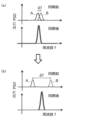
- 230000001360 synchronised effect Effects 0.000 description 20
- 230000010355 oscillation Effects 0.000 description 17
- 238000010586 diagram Methods 0.000 description 9
- 238000005259 measurement Methods 0.000 description 7
- 238000001228 spectrum Methods 0.000 description 7
- 238000000034 method Methods 0.000 description 6
- 238000004519 manufacturing process Methods 0.000 description 5
- 230000003993 interaction Effects 0.000 description 4
- 230000003595 spectral effect Effects 0.000 description 4
- 230000008859 change Effects 0.000 description 3
- XEEYBQQBJWHFJM-UHFFFAOYSA-N iron Substances [Fe] XEEYBQQBJWHFJM-UHFFFAOYSA-N 0.000 description 3
- 238000002474 experimental method Methods 0.000 description 2
- 238000005457 optimization Methods 0.000 description 2
- ZOXJGFHDIHLPTG-UHFFFAOYSA-N Boron Chemical compound [B] ZOXJGFHDIHLPTG-UHFFFAOYSA-N 0.000 description 1
- 229910045601 alloy Inorganic materials 0.000 description 1
- 239000000956 alloy Substances 0.000 description 1
- 229910052796 boron Inorganic materials 0.000 description 1
- 239000003990 capacitor Substances 0.000 description 1
- 230000000694 effects Effects 0.000 description 1
- 230000005294 ferromagnetic effect Effects 0.000 description 1
- 239000003302 ferromagnetic material Substances 0.000 description 1
- 229910052742 iron Inorganic materials 0.000 description 1
- 238000012986 modification Methods 0.000 description 1
- 230000004048 modification Effects 0.000 description 1
- 239000004065 semiconductor Substances 0.000 description 1
Images


Classifications
-
- H—ELECTRICITY
- H01—ELECTRIC ELEMENTS
- H01L—SEMICONDUCTOR DEVICES NOT COVERED BY CLASS H10
- H01L29/00—Semiconductor devices adapted for rectifying, amplifying, oscillating or switching, or capacitors or resistors with at least one potential-jump barrier or surface barrier, e.g. PN junction depletion layer or carrier concentration layer; Details of semiconductor bodies or of electrodes thereof ; Multistep manufacturing processes therefor
- H01L29/66—Types of semiconductor device ; Multistep manufacturing processes therefor
- H01L29/82—Types of semiconductor device ; Multistep manufacturing processes therefor controllable by variation of the magnetic field applied to the device
-
- H—ELECTRICITY
- H03—ELECTRONIC CIRCUITRY
- H03B—GENERATION OF OSCILLATIONS, DIRECTLY OR BY FREQUENCY-CHANGING, BY CIRCUITS EMPLOYING ACTIVE ELEMENTS WHICH OPERATE IN A NON-SWITCHING MANNER; GENERATION OF NOISE BY SUCH CIRCUITS
- H03B15/00—Generation of oscillations using galvano-magnetic devices, e.g. Hall-effect devices, or using superconductivity effects
-
- H—ELECTRICITY
- H10—SEMICONDUCTOR DEVICES; ELECTRIC SOLID-STATE DEVICES NOT OTHERWISE PROVIDED FOR
- H10N—ELECTRIC SOLID-STATE DEVICES NOT OTHERWISE PROVIDED FOR
- H10N50/00—Galvanomagnetic devices
- H10N50/10—Magnetoresistive devices
Description

2 パーマロイ層(NiFeB)
3 トンネル障壁層(MgO)
4 磁化自由層(FeB)
10 スピントルク発振素子(STO)
12 直流電源
13 高周波信号発生器
14 スペクトラムアナライザ
15 パーソナルコンピューター(PC)
16 パワーディバイダ
Claims (7)
- CoFeBを含む磁化固定層と、MgOを含むトンネル障壁層と、FeBからなる磁化自由層が順番に積層された積層構造において、前記磁化固定層と前記トンネル障壁層との間に各々に接するように配置したNiFeBを含むパーマロイ層を備える、スピントルク発振素子。
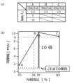
- 前記NiFeBにおけるNi組成比は76~85at%の範囲にある、請求項1に記載のスピントルク発振素子。
- 前記パーマロイ層は略5Åの厚さを有する、請求項1または2に記載のスピントルク発振素子。
- 前記磁化固定層は略23Åの厚さを有し、前記トンネル障壁層は略10Åの厚さを有し、前記磁化自由層は略50Åの厚さを有する、請求項1~3のいずれか1項に記載のスピントルク発振素子。
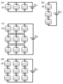
- 請求項1~4のいずれか1項に記載の複数のスピントルク発振素子を直列、並列、または直並列に配列したスピントルク発振素子アレイ。
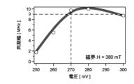
- 前記複数のスピントルク発振素子の同期幅は、9~11MHzの範囲にある、請求項5に記載のスピントルク発振素子アレイ。
- 前記複数のスピントルク発振素子に印加する磁界が360~390mTで、直流電圧が270~300mVの場合に前記同期幅が得られる、請求項6に記載のスピントルク発振素子アレイ。
Priority Applications (2)
| Application Number | Priority Date | Filing Date | Title |
|---|---|---|---|
| JP2018218165A JP7258332B2 (ja) | 2018-11-21 | 2018-11-21 | スピントルク発振素子 |
| PCT/JP2019/036543 WO2020105263A1 (ja) | 2018-11-21 | 2019-09-18 | スピントルク発振素子 |
Applications Claiming Priority (1)
| Application Number | Priority Date | Filing Date | Title |
|---|---|---|---|
| JP2018218165A JP7258332B2 (ja) | 2018-11-21 | 2018-11-21 | スピントルク発振素子 |
Publications (3)
| Publication Number | Publication Date |
|---|---|
| JP2020088088A JP2020088088A (ja) | 2020-06-04 |
| JP2020088088A5 JP2020088088A5 (ja) | 2021-11-25 |
| JP7258332B2 true JP7258332B2 (ja) | 2023-04-17 |
Family
ID=70774213
Family Applications (1)
| Application Number | Title | Priority Date | Filing Date |
|---|---|---|---|
| JP2018218165A Active JP7258332B2 (ja) | 2018-11-21 | 2018-11-21 | スピントルク発振素子 |
Country Status (2)
| Country | Link |
|---|---|
| JP (1) | JP7258332B2 (ja) |
| WO (1) | WO2020105263A1 (ja) |
Families Citing this family (4)
| Publication number | Priority date | Publication date | Assignee | Title |
|---|---|---|---|---|
| WO2019244662A1 (ja) * | 2018-06-19 | 2019-12-26 | ソニーセミコンダクタソリューションズ株式会社 | 磁気記憶素子、磁気ヘッド、磁気記憶装置、電子機器、及び磁気記憶素子の製造方法 |
| CN111969954B (zh) * | 2020-08-12 | 2022-10-21 | 北京航空航天大学合肥创新研究院 | 一种基于滤波器的自旋纳米振荡器同步方法 |
| CN113097379B (zh) * | 2021-03-23 | 2024-01-12 | 西安交通大学 | 包括磁耦合的自旋振荡器阵列的振荡器装置及其制造方法 |
| CN113823733A (zh) * | 2021-09-07 | 2021-12-21 | 北京航空航天大学合肥创新研究院(北京航空航天大学合肥研究生院) | 自旋力矩振荡器三维串并联同步阵列、振荡器及制备方法 |
Citations (5)
| Publication number | Priority date | Publication date | Assignee | Title |
|---|---|---|---|---|
| JP2002231904A (ja) | 2001-02-06 | 2002-08-16 | Mitsubishi Electric Corp | 磁気記憶装置および磁性体基板 |
| WO2009054182A1 (ja) | 2007-10-25 | 2009-04-30 | Fuji Electric Holdings Co., Ltd. | スピンバルブ素子及びその製造方法 |
| JP2012204682A (ja) | 2011-03-25 | 2012-10-22 | Toshiba Corp | 磁気発振素子及びスピン波装置 |
| JP2012253344A (ja) | 2011-05-31 | 2012-12-20 | Hgst Netherlands B V | 3端子スピントルク発振素子(sto) |
| JP2015060939A (ja) | 2013-09-18 | 2015-03-30 | 株式会社東芝 | 磁気記録装置 |
-
2018
- 2018-11-21 JP JP2018218165A patent/JP7258332B2/ja active Active
-
2019
- 2019-09-18 WO PCT/JP2019/036543 patent/WO2020105263A1/ja active Application Filing
Patent Citations (5)
| Publication number | Priority date | Publication date | Assignee | Title |
|---|---|---|---|---|
| JP2002231904A (ja) | 2001-02-06 | 2002-08-16 | Mitsubishi Electric Corp | 磁気記憶装置および磁性体基板 |
| WO2009054182A1 (ja) | 2007-10-25 | 2009-04-30 | Fuji Electric Holdings Co., Ltd. | スピンバルブ素子及びその製造方法 |
| JP2012204682A (ja) | 2011-03-25 | 2012-10-22 | Toshiba Corp | 磁気発振素子及びスピン波装置 |
| JP2012253344A (ja) | 2011-05-31 | 2012-12-20 | Hgst Netherlands B V | 3端子スピントルク発振素子(sto) |
| JP2015060939A (ja) | 2013-09-18 | 2015-03-30 | 株式会社東芝 | 磁気記録装置 |
Also Published As
| Publication number | Publication date |
|---|---|
| WO2020105263A1 (ja) | 2020-05-28 |
| JP2020088088A (ja) | 2020-06-04 |
Similar Documents
| Publication | Publication Date | Title |
|---|---|---|
| JP7258332B2 (ja) | スピントルク発振素子 | |
| Zeng et al. | High-power coherent microwave emission from magnetic tunnel junction nano-oscillators with perpendicular anisotropy | |
| Sharma et al. | Electrically connected spin-torque oscillators array for 2.4 GHz WiFi band transmission and energy harvesting | |
| Zeng et al. | Spin transfer nano-oscillators | |
| Bonetti et al. | Power and linewidth of propagating and localized modes in nanocontact spin-torque oscillators | |
| Silva et al. | Theory of thermally induced phase noise in spin torque oscillators for a high-symmetry case | |
| Prokopenko et al. | Spin-torque nano-oscillator as a microwave signal source | |
| US20070259209A1 (en) | Spin-torque devices | |
| JP5278876B2 (ja) | マイクロ波発振素子および検出素子 | |
| Thadani et al. | Strong linewidth variation for spin-torque nano-oscillators as a function of in-plane magnetic field angle | |
| JP2006295908A (ja) | マイクロ波伝送回路一体型マイクロ波発生素子及びマイクロ波伝送回路一体型マイクロ波検出素子 | |
| Berkov et al. | Micromagnetic simulations of magnetization dynamics in a nanowire induced by a spin-polarized current injected via a point contact | |
| Kendziorczyk et al. | Spin-wave-mediated mutual synchronization of spin-torque nano-oscillators: A micromagnetic study of multistable phase locking | |
| Rodríguez-Suárez et al. | Tunable misalignment of ferromagnetic and antiferromagnetic easy axes in exchange biased bilayers | |
| Yamamoto et al. | Zero-field spin torque oscillation in Co2 (Fe, Mn) Si with a point contact geometry | |
| US9407202B2 (en) | Spin-transfer torque type injection locking oscillator and design method thereof | |
| Zvezdin et al. | Spin currents and nonlinear dynamics of vortex spin torque nano-oscillators | |
| Huang et al. | Modelling high-power spin-torque oscillator with perpendicular magnetization in half-metallic Heusler alloy spin valve nanopillar | |
| Iacocca et al. | Destabilization of serially connected spin-torque oscillators via non-Adlerian dynamics | |
| Kumar et al. | Spin transfer torque induced domain wall oscillations in ferromagnetic nanowire with a nanoscale Dzyaloshinskii–Moriya interaction region | |
| Braganca et al. | Coherent and incoherent spin torque oscillations in a nanopillar magnetic spin-valve | |
| Wang et al. | Phase-locking of multiple magnetic droplets by a microwave magnetic field | |
| US8878618B2 (en) | Spin transfer oscillator | |
| Qu et al. | Phase-lock requirements in a serial array of spin transfer nano-oscillators | |
| Braganca et al. | Zero field high frequency oscillations in dual free layer spin torque oscillators |
Legal Events
| Date | Code | Title | Description |
|---|---|---|---|
| A521 | Request for written amendment filed |
Free format text: JAPANESE INTERMEDIATE CODE: A523 Effective date: 20181126 |
|
| A80 | Written request to apply exceptions to lack of novelty of invention |
Free format text: JAPANESE INTERMEDIATE CODE: A80 Effective date: 20181128 |
|
| A521 | Request for written amendment filed |
Free format text: JAPANESE INTERMEDIATE CODE: A523 Effective date: 20181204 |
|
| A521 | Request for written amendment filed |
Free format text: JAPANESE INTERMEDIATE CODE: A523 Effective date: 20211015 |
|
| A621 | Written request for application examination |
Free format text: JAPANESE INTERMEDIATE CODE: A621 Effective date: 20211015 |
|
| A131 | Notification of reasons for refusal |
Free format text: JAPANESE INTERMEDIATE CODE: A131 Effective date: 20221004 |
|
| A521 | Request for written amendment filed |
Free format text: JAPANESE INTERMEDIATE CODE: A523 Effective date: 20221124 |
|
| TRDD | Decision of grant or rejection written | ||
| A01 | Written decision to grant a patent or to grant a registration (utility model) |
Free format text: JAPANESE INTERMEDIATE CODE: A01 Effective date: 20230328 |
|
| A61 | First payment of annual fees (during grant procedure) |
Free format text: JAPANESE INTERMEDIATE CODE: A61 Effective date: 20230329 |
|
| R150 | Certificate of patent or registration of utility model |
Ref document number: 7258332 Country of ref document: JP Free format text: JAPANESE INTERMEDIATE CODE: R150 |