JP7200370B2 - logic circuit - Google Patents
logic circuit Download PDFInfo
- Publication number
- JP7200370B2 JP7200370B2 JP2021523069A JP2021523069A JP7200370B2 JP 7200370 B2 JP7200370 B2 JP 7200370B2 JP 2021523069 A JP2021523069 A JP 2021523069A JP 2021523069 A JP2021523069 A JP 2021523069A JP 7200370 B2 JP7200370 B2 JP 7200370B2
- Authority
- JP
- Japan
- Prior art keywords
- logic circuit
- serial data
- data bus
- printing device
- circuit package
- Prior art date
- Legal status (The legal status is an assumption and is not a legal conclusion. Google has not performed a legal analysis and makes no representation as to the accuracy of the status listed.)
- Active
Links
Images


Classifications
-
- G—PHYSICS
- G06—COMPUTING; CALCULATING OR COUNTING
- G06F—ELECTRIC DIGITAL DATA PROCESSING
- G06F13/00—Interconnection of, or transfer of information or other signals between, memories, input/output devices or central processing units
- G06F13/38—Information transfer, e.g. on bus
- G06F13/42—Bus transfer protocol, e.g. handshake; Synchronisation
- G06F13/4282—Bus transfer protocol, e.g. handshake; Synchronisation on a serial bus, e.g. I2C bus, SPI bus
- G06F13/4291—Bus transfer protocol, e.g. handshake; Synchronisation on a serial bus, e.g. I2C bus, SPI bus using a clocked protocol
-
- B—PERFORMING OPERATIONS; TRANSPORTING
- B41—PRINTING; LINING MACHINES; TYPEWRITERS; STAMPS
- B41J—TYPEWRITERS; SELECTIVE PRINTING MECHANISMS, i.e. MECHANISMS PRINTING OTHERWISE THAN FROM A FORME; CORRECTION OF TYPOGRAPHICAL ERRORS
- B41J2/00—Typewriters or selective printing mechanisms characterised by the printing or marking process for which they are designed
- B41J2/005—Typewriters or selective printing mechanisms characterised by the printing or marking process for which they are designed characterised by bringing liquid or particles selectively into contact with a printing material
- B41J2/01—Ink jet
- B41J2/17—Ink jet characterised by ink handling
- B41J2/175—Ink supply systems ; Circuit parts therefor
- B41J2/17503—Ink cartridges
- B41J2/17526—Electrical contacts to the cartridge
- B41J2/1753—Details of contacts on the cartridge, e.g. protection of contacts
-
- B—PERFORMING OPERATIONS; TRANSPORTING
- B41—PRINTING; LINING MACHINES; TYPEWRITERS; STAMPS
- B41J—TYPEWRITERS; SELECTIVE PRINTING MECHANISMS, i.e. MECHANISMS PRINTING OTHERWISE THAN FROM A FORME; CORRECTION OF TYPOGRAPHICAL ERRORS
- B41J2/00—Typewriters or selective printing mechanisms characterised by the printing or marking process for which they are designed
- B41J2/005—Typewriters or selective printing mechanisms characterised by the printing or marking process for which they are designed characterised by bringing liquid or particles selectively into contact with a printing material
- B41J2/01—Ink jet
- B41J2/17—Ink jet characterised by ink handling
- B41J2/175—Ink supply systems ; Circuit parts therefor
- B41J2/17503—Ink cartridges
- B41J2/17543—Cartridge presence detection or type identification
- B41J2/17546—Cartridge presence detection or type identification electronically
-
- B—PERFORMING OPERATIONS; TRANSPORTING
- B41—PRINTING; LINING MACHINES; TYPEWRITERS; STAMPS
- B41J—TYPEWRITERS; SELECTIVE PRINTING MECHANISMS, i.e. MECHANISMS PRINTING OTHERWISE THAN FROM A FORME; CORRECTION OF TYPOGRAPHICAL ERRORS
- B41J2/00—Typewriters or selective printing mechanisms characterised by the printing or marking process for which they are designed
- B41J2/005—Typewriters or selective printing mechanisms characterised by the printing or marking process for which they are designed characterised by bringing liquid or particles selectively into contact with a printing material
- B41J2/01—Ink jet
- B41J2/17—Ink jet characterised by ink handling
- B41J2/175—Ink supply systems ; Circuit parts therefor
- B41J2/17503—Ink cartridges
- B41J2/17553—Outer structure
-
- G—PHYSICS
- G03—PHOTOGRAPHY; CINEMATOGRAPHY; ANALOGOUS TECHNIQUES USING WAVES OTHER THAN OPTICAL WAVES; ELECTROGRAPHY; HOLOGRAPHY
- G03G—ELECTROGRAPHY; ELECTROPHOTOGRAPHY; MAGNETOGRAPHY
- G03G21/00—Arrangements not provided for by groups G03G13/00 - G03G19/00, e.g. cleaning, elimination of residual charge
- G03G21/16—Mechanical means for facilitating the maintenance of the apparatus, e.g. modular arrangements
- G03G21/18—Mechanical means for facilitating the maintenance of the apparatus, e.g. modular arrangements using a processing cartridge, whereby the process cartridge comprises at least two image processing means in a single unit
- G03G21/1875—Mechanical means for facilitating the maintenance of the apparatus, e.g. modular arrangements using a processing cartridge, whereby the process cartridge comprises at least two image processing means in a single unit provided with identifying means or means for storing process- or use parameters, e.g. lifetime of the cartridge
- G03G21/1878—Electronically readable memory
-
- G—PHYSICS
- G06—COMPUTING; CALCULATING OR COUNTING
- G06F—ELECTRIC DIGITAL DATA PROCESSING
- G06F13/00—Interconnection of, or transfer of information or other signals between, memories, input/output devices or central processing units
- G06F13/38—Information transfer, e.g. on bus
- G06F13/382—Information transfer, e.g. on bus using universal interface adapter
-
- H—ELECTRICITY
- H04—ELECTRIC COMMUNICATION TECHNIQUE
- H04N—PICTORIAL COMMUNICATION, e.g. TELEVISION
- H04N1/00—Scanning, transmission or reproduction of documents or the like, e.g. facsimile transmission; Details thereof
- H04N1/00127—Connection or combination of a still picture apparatus with another apparatus, e.g. for storage, processing or transmission of still picture signals or of information associated with a still picture
- H04N1/00204—Connection or combination of a still picture apparatus with another apparatus, e.g. for storage, processing or transmission of still picture signals or of information associated with a still picture with a digital computer or a digital computer system, e.g. an internet server
- H04N1/00209—Transmitting or receiving image data, e.g. facsimile data, via a computer, e.g. using e-mail, a computer network, the internet, I-fax
- H04N1/00214—Transmitting or receiving image data, e.g. facsimile data, via a computer, e.g. using e-mail, a computer network, the internet, I-fax details of transmission
Description
背景
アイ・スクエアド・シー(I2C、又はI2C(その表記が本明細書で採用される))プロトコル及びシリアル・ペリフェラル・インターフェース(SPI)プロトコルのようなシリアル・データ・バス・プロトコルにより、少なくとも1つの「マスター」集積回路(IC)が、少なくとも1つの「スレーブ」ICと通信することが可能となり、例えば、バスI2C、及び他の通信プロトコルを介して、クロック周期に従ってデータを通信することが可能となる。例えば、電圧信号が生成されることができ、この場合、電圧の値は、データと関連付けられる。例えば、x以上の電圧値は論理「1」を示すことができる一方で、x電圧未満の電圧値は論理「0」を示すことができ、この場合、xは所定の数値である。一連のクロック周期のそれぞれにおいて適切な電圧を生成することにより、データは、バス又は別の通信リンクを介して伝達され得る。
BACKGROUND With serial data bus protocols such as the I Squared Sea ( I2C, or I2C (as that notation is adopted herein)) protocol and the Serial Peripheral Interface (SPI) protocol, At least one "master" integrated circuit (IC) is enabled to communicate with at least one "slave" IC, communicating data according to the clock cycle, e.g., via bus I2C and other communication protocols. becomes possible. For example, a voltage signal can be generated, where the voltage value is associated with the data. For example, a voltage value greater than or equal to x may indicate a logic '1', while a voltage value less than x voltage may indicate a logic '0', where x is a predetermined numerical value. By generating the appropriate voltages on each of a series of clock cycles, data can be communicated over a bus or another communication link.
幾つかの2D及び3D印刷システムは、印刷材料容器(例えば、インクジェット・カートリッジ、トナー・カートリッジ、インク補給品、構築材料補給品など)、インクジェット・プリントヘッド・アセンブリ、及び同類の物のような、1つ又は複数の交換可能な印刷装置構成要素を含む。幾つかの例において、交換可能な印刷装置構成要素(単数または複数)と関連付けられる論理回路は、当該交換可能な印刷装置構成要素が装着される印刷装置の論理回路と通信し、例えば、それらの正体(身元、同一性)、容量、ステータス、及び同類の物のような情報を伝達する。 Some 2D and 3D printing systems include printing material containers (e.g., inkjet cartridges, toner cartridges, ink supplies, build material supplies, etc.), inkjet printhead assemblies, and the like. Contains one or more replaceable printing device components. In some examples, the logic associated with the replaceable printing device component(s) communicates with the logic of the printing device to which the replaceable printing device component is attached, e.g. Conveys information such as identity (identity, identity), capacity, status, and the like.
幾つかの例において、これらの通信は、I2C通信を利用する。係る例において、マスターICは一般に、印刷装置の一部として提供されることができ(「ホスト」と呼ばれ得る)、交換可能な印刷装置構成要素は、「スレーブ」ICを含むが、これは必ずしも全ての例における事例ではない。I2C通信リンクに接続された複数のスレーブIC(例えば、異なる色の印刷剤の容器)が存在することができる。スレーブIC(単数または複数)は、印刷システムの論理回路からの要求に応答する前にデータ操作を行うための論理回路を含むことができる。 In some examples, these communications utilize I2C communications. In such examples, a master IC can generally be provided as part of a printing device (may be referred to as a "host"), and replaceable printing device components include "slave" ICs, which are Not necessarily the case in every instance. There may be multiple slave ICs (eg containers of different colored printing agents) connected to the I2C communication link. The slave IC(s) may include logic circuitry for performing data manipulations prior to responding to requests from the printing system logic circuitry.
幾つかの例において、シリアル・バスに沿って取り付けられるスレーブ・デバイスの物理的位置を検出することが意図され得る。例えば、交換可能な印刷装置構成要素のようなデバイスが、印刷装置内の特定の指定された物理的場所を占有することが意図され得る。例えば、シリアル・バスに取り付けられたインク供給デバイスを備える印刷装置において、例えば、ブラック・カートリッジ、イエロー・カートリッジ、シアン・カートリッジ及びマゼンタ・カートリッジ用の予想される場所が存在することができ、それらのそれぞれは、通信プロトコル下で特定のアドレスを有することができる。特定のインク色のカートリッジが誤って装着されたか否か、又は交換されたか否かを検出することにより、間違った色または意図されていない色による印刷が防止され得る。従来の特許情報開示は、特許文献1である。 In some examples, it may be intended to detect the physical location of slave devices attached along a serial bus. For example, a device such as a replaceable printing device component may be intended to occupy a particular designated physical location within the printing device. For example, in a printing device with an ink supply device attached to a serial bus, there may be expected locations for, for example, a black cartridge, a yellow cartridge, a cyan cartridge and a magenta cartridge, which Each can have a specific address under the communication protocol. By detecting whether a cartridge of a particular ink color has been incorrectly installed or replaced, printing with the wrong or unintended color can be prevented. A conventional patent information disclosure is US Pat.
さて、制限しない例が、添付図面に関連して説明される。 A non-limiting example will now be described with reference to the accompanying drawings.
詳細な説明
本明細書において、I2C通信の応用形態に関する幾つかの例が、印刷装置の文脈で説明される。しかしながら、全ての例が係る応用形態に制限されず、本明細書で提示される原理の少なくとも幾つかは、他の文脈で使用され得る。
DETAILED DESCRIPTION Several examples of I2C communication applications are described herein in the context of printing devices. However, all examples are not limited to such applications, and at least some of the principles presented herein can be used in other contexts.
幾つかの例において、印刷装置内の論理回路は、通信インターフェースを介して、交換可能な印刷装置構成要素と関連付けられた論理回路から情報を受け取ることができるか、及び/又は交換可能な印刷装置構成要素にコマンドを送ることができる。例示的な印刷装置は、インクジェット・プリンタ、乾式トナー・プリンタ、液体トナー・プリンタ、3D粉末床インクジェット・プリンタなどのような、二次元イメージング装置および三次元積層造形装置を含む。例示的な印刷装置構成要素は、インク・タンク;インク・ボトル;プリントヘッド;インクジェット・プリントヘッド・カートリッジ;乾式トナー・リザーバ;乾式トナー・カートリッジ;光導電体カートリッジ;プロセス・カートリッジ;液体トナー・リザーバ;インク、刺激剤、接着剤、阻害剤などを含む三次元印刷剤;三次元印刷構築材料;印刷装置サービス構成要素;及び/又はホスト印刷装置に対して交換可能であることができ且つ印刷材料を含むことができる又は含むことができない任意の他の構成要素を含む。本開示において、印刷材料または印刷剤は、インク、乾式トナー又は液体トナー、三次元印刷剤、三次元構築材料(プラスチック、金属など)、ファイバ(線維)などを含むことができる。上述されたリザーバは、着色された印刷材料を含むことができる。 In some examples, logic circuitry within the printing device can receive information from logic circuitry associated with replaceable printing device components via a communication interface and/or You can send commands to components. Exemplary printing devices include two-dimensional imaging devices and three-dimensional additive manufacturing devices, such as inkjet printers, dry toner printers, liquid toner printers, 3D powder bed inkjet printers, and the like. Exemplary printing device components include ink tanks; ink bottles; printheads; inkjet printhead cartridges; dry toner reservoirs; dry toner cartridges; three-dimensional printing agents including inks, stimulants, adhesives, inhibitors, etc.; three-dimensional printing building materials; printing device service components; including any other component that may or may not contain In this disclosure, printing materials or agents can include inks, dry or liquid toners, three-dimensional printing agents, three-dimensional building materials (plastics, metals, etc.), fibers, and the like. The reservoirs described above may contain pigmented printing material.
印刷装置と当該装置に装着された交換可能な印刷装置構成要素との間の通信は、様々な機能を提供することができる。例えば、交換可能な印刷装置構成要素の正体(身元)、機能および/またはステータス、及び/又はそれと関連付けられた論理回路は、通信インターフェースを介して、印刷装置の論理回路に伝達(通信)され得る。例えば、印刷剤容器と関連付けられた(又は当該容器上に又は当該容器内に設けられた)論理回路は、製造番号および/または商標(ブランド)のような正体、及び/又は色(カラー)、カラー・マップ、カラー・マップ再構成レシピ、最大印刷剤容量または機能のような識別特性を、当該容器が装着される印刷装置に伝達することができ、例えば、特許文献2、特許文献3、特許文献4、又は特許文献5を参照されたい。充填レベルのようなステータスは、例えば、印刷装置がユーザに充填レベルの表示を生成することができるように、通信インターフェースを介して提供され得る。幾つかの例において、検証過程が、印刷装置により実行され得る。例えば、印刷装置は、交換可能な印刷装置構成要素が公認の供給元に由来するかを検証して、その品質を保証することができる。例えば、交換可能な印刷装置構成要素と関連付けられた論理回路は、秘密鍵を格納することができ、プリンタに対する認証暗号応答を生成するためのセッション鍵、セッション鍵識別子および/またはメッセージ確認コードを生成するように構成されることができ、例えば、特許文献6を参照されたい。また、当該論理回路は更に、所定の比較的短い時間ウィンドウ内で応答を計算するための専用ハードウェアのような認証メカニズムも含むことができ、例えば、特許文献7を参照されたい。幾つかの例において、検証過程は、交換可能な印刷装置構成要素および/またはそれと関連付けられた論理回路が予想通りに機能していることを保証するために一貫性チェックを含むことができる。 Communication between a printing device and replaceable printing device components attached to the device can provide a variety of functions. For example, the identity, function and/or status of a replaceable printing device component, and/or logic circuitry associated therewith, may be communicated to the logic circuitry of the printing device via a communication interface. . For example, a logic circuit associated with (or provided on or within) a printing agent container may identify a serial number and/or identity, such as a brand, and/or color, Identification characteristics, such as color maps, color map reconstruction recipes, maximum printing material capacity or functions, can be communicated to the printing device to which the container is attached, e.g. See Document 4 or Patent Document 5. Status, such as fill level, can be provided via a communication interface, for example, so that the printing device can generate an indication of fill level to the user. In some examples, the verification process may be performed by the printing device. For example, a printing device can verify that replaceable printing device components come from an authorized source to ensure their quality. For example, logic circuitry associated with a replaceable printing device component can store a private key and generate a session key, session key identifier and/or message verification code for generating an authenticated cryptographic response to the printer. See, for example, US Pat. The logic may also include an authentication mechanism such as dedicated hardware for computing responses within a predetermined relatively short time window, see for example US Pat. In some examples, the verification process can include consistency checks to ensure that the replaceable printing device components and/or logic circuits associated therewith are functioning as expected.
次に、タスクを実行するための命令が、通信インターフェースを介して、印刷装置と関連付けられた論理回路から印刷装置構成要素の論理回路へ送られ得る。例えば、これらは、認証機能または暗号化機能、印刷材料レベル検知機能、印刷タスク、又は他のタスクを実行するための命令を含むことができる。 Instructions to perform the task can then be sent from the logic associated with the printing device to the logic of the printing device component via the communications interface. For example, these may include instructions for performing authentication or encryption functions, printing material level detection functions, printing tasks, or other tasks.
後述される例の少なくとも幾つかにおいて、論理回路パッケージが説明される。論理回路パッケージは、例えばそれに取り付けられている交換可能な印刷装置構成要素と関連付けられ得る、又はそのハウジング内に少なくとも部分的に構成されることができ、印刷装置の一部として提供されるバスを介して、データを印刷装置コントローラとやりとりするように適合される。 In at least some of the examples described below, logic circuit packages are described. A logic circuit package may, for example, be associated with a replaceable printing device component attached to it, or may be configured at least partially within its housing, and may include a bus provided as part of the printing device. adapted to communicate data to and from the printing device controller via the
「論理回路パッケージ」は、当該用語が本明細書で使用される際、互いに相互接続され得る又は互いに通信可能にリンクされ得る1つ又は複数の論理回路を意味する。2つ以上の論理回路が提供される場合、これらは単一ユニットとしてカプセル化され得る、又は別個にカプセル化され得る、又はカプセル化されない、又はそれらの幾つかの組み合わせであることができる。各パッケージは、シリアル・バス・インターフェースを介して通信するように構成され得る。 "Logic circuit package," as that term is used herein, means one or more logic circuits that can be interconnected or communicatively linked together. Where more than one logic circuit is provided, these may be encapsulated as a single unit, or may be separately encapsulated or non-encapsulated, or some combination thereof. Each package may be configured to communicate via a serial bus interface.
幾つかの例において、各論理回路パッケージには、少なくとも1つのプロセッサ及びメモリが設けられる。一例において、論理回路パッケージは、マイクロコントローラ又はセキュア・マイクロコントローラであることができる、又はマイクロコントローラ又はセキュア・マイクロコントローラとして機能することができる。使用中、論理回路パッケージは、交換可能な印刷装置構成要素に付着され得る、又は交換可能な印刷装置構成要素と一体化され得る。 In some examples, each logic circuit package is provided with at least one processor and memory. In one example, the logic circuit package can be a microcontroller or a secure microcontroller, or can function as a microcontroller or a secure microcontroller. In use, the logic circuit package can be attached to a replaceable printing device component or integrated with a replaceable printing device component.
幾つかの例において、論理回路パッケージは、ホスト(例えば、印刷装置)からの様々なタイプの要求(又はコマンド)に応答することができる。要求は、データ、例えば識別情報および/または認証情報に対する要求(例えば、「読み出し」要求)を含むことができる。他の例において、要求は、「書き込み」要求を含むことができる。ホストからの別の要求は、少なくとも1つの測定を実行する、又は印刷タスク又は同類の物を実行するような、動作を実行するための要求であることができる。別のタイプの要求は、データ処理動作のための要求であることができる。 In some examples, a logic circuit package can respond to various types of requests (or commands) from a host (eg, a printing device). Requests can include requests for data, such as identification and/or authentication information (eg, “read” requests). In another example, the request can include a "write" request. Another request from the host can be a request to perform an action, such as performing at least one measurement, or performing a print task or the like. Another type of request can be a request for a data processing operation.
相互作用(対話)の例において、ホストは、交換可能な印刷装置構成要素と関連付けられた論理回路パッケージにコマンドを送ることができ、当該論理回路パッケージは、当該コマンドを実行して、結果として生じるデータをメモリ(幾つかの例において、バッファ及び/又はメモリの特定のレジスタ)へロードすることができる。ホストは、応答を読み出すために更なるコマンドを送ることができ、それにより当該応答が、接続されたバスを介してシリアル・データとして伝送される。係るプロセス(過程)は例えば、論理回路パッケージのメモリに保持されたデータを取得するために使用され得る。例えば、第1の要求は、そのパッケージの識別子の要求であることができ、当該パッケージが識別子をメモリ・バッファへロードするという結果になることができる。その後の「読み出し」要求は、データが当該バッファから読み出されて、シリアル・データ信号として伝送されるという結果になることができる。 In an interaction example, the host can send a command to a logic circuit package associated with a replaceable printing device component, which executes the command and produces a resulting Data can be loaded into memory (in some examples, buffers and/or specific registers in memory). The host can send further commands to read the response, which is then transmitted as serial data over the attached bus. Such processes may be used, for example, to retrieve data held in memory of a logic circuit package. For example, the first request may be for the package's identifier, and may result in the package loading the identifier into a memory buffer. Subsequent "read" requests can result in data being read from the buffer and transmitted as a serial data signal.
少なくとも幾つかの例において、複数の係る論理回路パッケージ(それらの各々が異なる交換可能な印刷装置構成要素と関連付けられ得る)は、I2Cバスに接続され得る。 In at least some examples, multiple such logic packages (each of which may be associated with a different replaceable printing device component) may be connected to the I2C bus.
図1は、印刷システム100の一例である。印刷システム100は、通信リンク106を介して、交換可能な印刷装置構成要素104と通信する印刷装置102を含む。明確にするために、交換可能な印刷装置構成要素104は印刷装置102の外部として示されるが、幾つかの例において、交換可能な印刷装置構成要素104は、印刷装置内に収容され得る。印刷装置102は、任意のタイプの2D印刷装置または3D印刷装置であることができる。
FIG. 1 is an example of a
交換可能な印刷装置構成要素104は例えば、印刷装置102の消費可能資源、又は印刷装置102の寿命より短い(幾つかの例において、大幅に短い)寿命を有する可能性がある構成要素を含むことができる。例えば、当該印刷装置構成要素104は、インク、トナー、3D印刷剤、又は3D印刷構築粉末を物理的に貯蔵することができ、実質的な枯渇後に交換されることが意図され得る。交換可能な印刷装置構成要素104は例えば、印刷材料容器またはカートリッジ(3D印刷用の構築材料容器、又は2D又は3D印刷用の液体印刷剤容器であることができる)を含むことができる。幾つかの例において、交換可能な印刷装置構成要素104は、プリントヘッド又は他の吐出構成要素を含むことができる。この例において、単一の交換可能な印刷装置構成要素104が示されるが、他の例において、例えば、異なる色の印刷剤容器、プリントヘッド(当該容器に一体化され得る)、又は同類の物を含む複数の交換可能な印刷装置構成要素が存在することができる。
Replaceable
幾つかの例において、通信リンク106は、シリアル・バス、例えばI2C対応バス又はI2C互換性バス(本明細書において以降は、I2Cバス)を含むことができる。
In some examples,
図2は、図1の交換可能な印刷装置構成要素104を提供することができる交換可能な印刷装置構成要素200の一例を示す。交換可能な印刷装置構成要素200は、論理回路パッケージ204へ統合(一体化)されたデータ・インターフェース202を含む。交換可能な印刷装置構成要素200の使用中、論理回路パッケージ204は、データ・インターフェース202を介して受け取ったデータを復号する。データ・インターフェース202は、I2Cインターフェースを含むことができる。
FIG. 2 illustrates an example of a replaceable
幾つかの例において、論理回路パッケージ204は更に、データ・インターフェース202を介して伝送するためのデータを符号化するように構成され得る。幾つかの例において、単一の構成要素200に対して設けられた2つ以上のデータ・インターフェース202が存在することができる。
In some examples,
幾つかの例において、論理回路パッケージ204は、I2C通信における「スレーブ」としての役割を果たすように構成され得る。
In some examples,
この例における交換可能な印刷装置構成要素200は、上述した印刷材料の例の何れかを収容することができる印刷材料リザーバ206を含む。
The replaceable
図3は、印刷装置300の一例を示す。印刷装置300は、図1の印刷装置102を提供することができる。印刷装置300は、交換可能な印刷装置構成要素と通信するためのインターフェース302及び通信バス306を含むコントローラ304を含む。コントローラ304は論理回路を含む。幾つかの例において、インターフェース302は、I2Cインターフェースであり、通信バス306は、I2C対応通信バスである。
FIG. 3 shows an example of a
幾つかの例において、コントローラ304は、I2C通信において、ホスト又はマスターとしての役割を果たすように構成され得る。コントローラ304は、少なくとも1つの交換可能な印刷装置構成要素200にコマンドを生成および送信することができ、それから応答を受信して、受信した応答を復号することができる。
In some examples,
係る印刷装置102、300、及び交換可能な印刷装置構成要素(単数または複数)104、200、及び/又はその論理回路パッケージは、別個に製造され得る、及び/又は販売され得る。一例において、ユーザは、印刷装置102、300を手に入れることができ、長年にわたって当該装置102、300を持ち続けることができる一方で、複数の交換可能な印刷装置構成要素104、200が、それらの長年において、例えば印刷剤が印刷出力を生成する際に使用される場合、購入され得る。従って、印刷装置102、300と交換可能な印刷装置構成要素104、200との間で少なくとも或る程度の上位互換性および/または下位互換性が存在する場合がある。
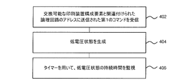
図4は、交換可能な印刷装置構成要素と関連付けられた論理回路パッケージにより実行され得る方法の一例である。幾つかの例において、方法は、交換可能な印刷装置構成要素が装着される印刷装置が交換可能な印刷装置構成要素の物理的位置を求めることができるように、実行され得る。本明細書で説明される方法は、シリアル・ペリフェラル・インターフェース(SPI)プロトコルのような、I2C以外の通信プロトコルと共に使用され得るが、留意されるべきは、I2Cプロトコルにおいて、複数のデバイスは、それらの物理的位置または順序を即座に求める又は指定する任意の手段なしに、単一のバス上にシリアル(直列)に接続される。しかしながら、例えばSPIを考察する場合、2つの配線構成、並列およびデイジー・チェーンが存在する。並列配線構成において、各「スレーブ」論理回路に専用の別個のライン(線)が存在し、デイジー・チェーン構成において、デバイスは特定の順序で逐次に配線され、そのため、それらの相対的な位置は、何か他の方法で有効化される場合がある。従って、本明細書で説明される方法は、I2Cのような、デバイスの物理的位置を検証することが難しいプロトコルを用いる特定のユーティリティを有することができる。しかしながら、それは、それに制限されない。 FIG. 4 is an example of a method that may be performed by a logic circuit package associated with a replaceable printing device component. In some examples, the method may be performed such that a printing device to which the replaceable printing device component is attached can determine the physical location of the replaceable printing device component. It should be noted that although the methods described herein may be used with communication protocols other than I2C, such as the Serial Peripheral Interface (SPI) protocol, in the I2C protocol, multiple devices communicate with their are connected serially on a single bus without any means of immediately determining or specifying their physical location or order. However, when considering SPI for example, there are two wiring configurations, parallel and daisy chain. In a parallel wiring configuration there is a separate line dedicated to each "slave" logic circuit, and in a daisy chain configuration the devices are wired serially in a particular order so that their relative positions are , may be enabled in some other way. Thus, the methods described herein can have particular utility with protocols such as I2C, where it is difficult to verify the physical location of a device. However, it is not so limited.
ブロック402は、シリアル・データ・バス(例えば、I2Cバス)を介して、交換可能な印刷装置構成要素と関連付けられた論理回路のアドレスに送信された第1のコマンドを受信することを含む。幾つかの例において、第1のコマンドは、動作モードの指示であることができる。幾つかの例において、第1のコマンドは時間期間の指示であることができる。アドレスは、論理回路/論理回路パッケージに格納された及び/又は配線で接続されたI2Cバス・インターフェース・アドレスであることができる。第1のコマンドは、印刷装置のコントローラにより、当該アドレスに送信され得る。第1のコマンドは、所定のコマンドであることができる。
ブロック404は、論理回路により、シリアル・データ・バス上に低電圧状態を生成することを含む。以下でより詳細に説明されるように、これは実質上、シリアル・データ・バス(より具体的には、シリアル・データ・バスのデータ・ライン)と接地との間の接続を提供することを含むことができる。一例において、低電圧は、公称の接地または約0Vのような基準電圧である。以下でも説明されるように、低電圧は、高い又はデフォルトの電圧状態または電圧状況より低い。
ブロック406は、論理回路のタイマーを用いて、低電圧状態の持続時間を監視することを含む。タイマーは、論理回路の内部の一体型タイマーからなることができ、例えば、タイマーとして働くように構成された抵抗容量(RC)回路、カウンターと共に構成された論理ゲート、水晶発振器またはリング発振器、位相ロック・ループ(フェーズロックド・ループとしても知られる)又は同類の物、又は交換可能な印刷装置構成要素に関連して設けられた論理回路の一部を論理的に構成する任意のタイマーを含む。タイマーは、シリアル・データ・バス上にクロック信号が無くても提供される内部クロック信号を提供することができる。タイマーは、計数(カウント)することができ、ひいては第1のコマンドで指定されたタイマー期間の持続時間の決定を可能にする。
タイマーは、コマンドの時間期間を測定することに捧げられ得る。特定の例において、タイマーは、I2Cクロック・サイクル及び/又はホスト装置または論理回路の中央処理装置の処理サイクルのような、動作しているI2C論理回路パッケージにおける他の汎用サイクルに関係無い時間を測定することに捧げられる。例えば、タイマーは、クロック周波数より速く計数するように構成されることができ、クロック信号のタイミングに関係無く、計数することを開始および停止することができる。タイマーは、論理回路/ホスト装置の中央処理装置のプロセッサ速度に関係無く計数するように構成されることができ、例えば中央処理装置に関係無い公称の仕様を有する。 A timer may be dedicated to measuring the time duration of the command. In a particular example, the timer measures time independent of other general cycles in the active I2C logic circuit package, such as I2C clock cycles and/or processing cycles of the host device or the central processing unit of the logic circuit. Dedicated to doing. For example, the timer can be configured to count faster than the clock frequency and can start and stop counting regardless of the timing of the clock signal. The timer can be configured to count regardless of the processor speed of the central processing unit of the logic circuit/host device, eg, having nominal specifications regardless of the central processing unit.
他の例において、論理回路/論理回路パッケージは、外部クロックのような外部タイマーを監視することに基づいて、又は特定の例において、時間期間の持続時間を求めるのに適切であることができる外部または内部の波形信号、発振(振動)信号などを監視することにより、時間期間を監視することができる。一例において、論理回路パッケージのタイマーは、論理回路と無線でリンクされたタイマーであることができる(そのため、1つのタイマーが、より多い論理回路により共用され得る)。 In other examples, the logic circuit/logic circuit package may be based on monitoring an external timer, such as an external clock, or in certain examples, may be suitable for determining the duration of a time period. Alternatively, the time period can be monitored by monitoring an internal waveform signal, oscillation (vibration) signal, or the like. In one example, the timer of the logic circuit package can be a timer wirelessly linked with the logic circuit (so one timer can be shared by more logic circuits).
方法は、シリアル・データ・バスが異なる及び/又はデフォルトの高い電圧状態または電圧状況になるような時間期間の終わりで、バスを解放すること、又は低電圧状態を解除することを含むことができる。これは例えば、接地への接続を遮断することを含む。時間期間外で、例えば第1のコマンドに応答して開始されるような時間期間の持続時間の前と後で、論理回路/論理回路パッケージは、高電圧状態を生成することができる。代案として、係る高電圧状態は、後述されるように、バス上に「プルアップ」抵抗を含むことにより生じるデフォルト状態であることができる。 The method includes releasing the bus or removing the low voltage state at the end of a period of time such that the serial data bus is in a different and /or default high voltage state or condition. can be done. This includes, for example, breaking the connection to ground. Outside the time period, for example before and after the duration of the time period as initiated in response to the first command, the logic circuit/logic circuit package can generate a high voltage state. Alternatively, such a high voltage state can be a default state caused by including a "pull-up" resistor on the bus, as described below.
例えば、I2Cデータ・バスを考察すると、これは、2つの通信ライン、即ちシリアル・データ・ライン(SDA)及びシリアル・クロック・ライン(SCL)を含む。SDA及びSCLは、電流源またはプルアップ抵抗を介して、正の電圧源に接続された双方向性ラインであることができる。 For example, consider an I2C data bus, which includes two communication lines, a serial data line (SDA) and a serial clock line (SCL). SDA and SCL can be bidirectional lines connected to a positive voltage source through current sources or pull-up resistors.
ライン上に信号がない場合(即ち、SCL上にクロック信号が無い、及び/又はデータ・ライン上にデータ信号が無い)、双方のラインは、高(HIGH)電圧状態のデフォルトにされ得る。高電圧状態の電圧の正確な値は、多くの動作因子に依存するが、幾つかの例において、例えば約3ボルトから6ボルトの間の数ボルトであることができる。従って、一般に「高」電圧は比較的低い場合があるが、これは、例えば1ボルト未満であることができるバスの「低」電圧状態に比べて高い。 If there is no signal on the line (ie, no clock signal on SCL and/or no data signal on the data line), both lines may default to a HIGH voltage state. The exact value of the high voltage state voltage depends on many operating factors, but in some instances can be a few volts, for example between about 3 and 6 volts. Thus, in general, the "high" voltage may be relatively low, which is higher than the "low" voltage state of the bus, which may be less than 1 volt, for example.
マスター/ホスト・デバイス(例えば、本文脈において、交換可能な印刷装置構成要素が装着される印刷装置の処理回路またはコントローラ)は、SCLラインの電圧を低(LOW)状態に引き下ろすことにより(例えば、接地への短絡を事実上提供するためのオープンドレイン構成を用いて)、クロック信号を生成することができる。例えば、スイッチ(電界効果トランジスタのような)が付勢されて(閉じられて)、低電圧状態をもたらすことができ、次いで、ライン上のプルアップ抵抗が電圧を高(HIGH)状態まで引っ張ることを可能にするように再び開かれる。他の例において、オープンコレクタ構成が使用されることができ、この場合、バイポーラ接合トランジスタ(BJT)が同様の効果のために使用され得る。プルダウン及び解放のタイミングは、マスター・デバイスの処理回路により制御されるクロック信号を提供する。 A master/host device (e.g., in this context, the processing circuitry or controller of the printing device to which the replaceable printing device component is attached) pulls the voltage on the SCL line to a LOW state (e.g., , using an open-drain configuration to effectively provide a short circuit to ground) to generate the clock signal. For example, a switch (such as a field effect transistor) can be energized (closed) to provide a low voltage state, and then a pull-up resistor on the line pulls the voltage to a HIGH state. is reopened to allow In another example, an open-collector configuration can be used, in which case a bipolar junction transistor (BJT) can be used to similar effect. The pull-down and release timings provide clock signals that are controlled by the processing circuitry of the master device.
データを伝送するために、マスター・デバイス又はスレーブ(この例において、交換可能な印刷装置構成要素と関連付けられた論理回路)は、電圧を低(LOW)に引っ張る(例えば、接地への接続を提供する)ことにより、又は電圧を「フロート高(HIGH)」にする(例えば、接地への接続を遮断する)ことにより、同様にSDA上の電圧を選択的に制御することができる。これは、クロック信号で、即ちI2Cプロトコルに従ってタイミングをとられ、SCLラインが高(HIGH)である際のSDAラインの状態が、少なくとも1つのデータ・ビットを提供する。通常、SCLが高(HIGH)である際にSDAラインが低(LOW)(及び安定)である場合、これはバイナリの0を示し、SCLが高(HIGH)(及び安定)である際にSDAラインが高(HIGH)である場合、これはバイナリの1を示すが、これは慣例であり、そのため、所与のシステムにおいて変更され得る。 To transmit data, a master device or slave (in this example, logic circuitry associated with a replaceable printing device component) pulls a voltage LOW (e.g., provides a connection to ground). Similarly, the voltage on SDA can be selectively controlled by letting the voltage "float HIGH" (eg, breaking the connection to ground). This is timed with a clock signal, ie according to the I2C protocol, the state of the SDA line when the SCL line is HIGH provides at least one data bit. Normally, when the SDA line is LOW (and stable) when SCL is HIGH, this indicates a binary 0, and when SCL is HIGH (and stable), the SDA line is LOW. When the line is HIGH, it indicates a binary 1, but this is a convention and so can be changed in a given system.
図4の方法の一例において、SCLラインが高である状態と一致するようにタイミングをとられるデータ信号を提供する代わりに、SCLラインの状態は考慮されない。実際には、電圧は、論理回路のタイマーにより監視される持続時間にわたって低に引っ張られ(やはり、例えば接地への接続を提供することにより)、次いで、「解放」される又はデフォルトの高(HIGH)状態になるようにされる(例えば、その接続を遮断することにより)。実際には、幾つかの実施形態において、低電圧状態の持続時間の少なくとも部分的にわたって、及び幾つかの例においてその全体にわたって、マスター・デバイスにより提供されるクロック信号が存在しない場合がある。 In one example of the method of FIG. 4, instead of providing a data signal timed to coincide with the state of the SCL line being high, the state of the SCL line is not considered. In practice, the voltage is pulled low (again, e.g., by providing a connection to ground) for a duration monitored by a timer in the logic circuit, and then "released" or default high (HIGH ) state (eg, by breaking its connection). In fact, in some embodiments, the clock signal provided by the master device may be absent for at least a portion, and in some instances throughout, the duration of the low voltage state.
上述されたように、この方法は、ここで図5に関連して説明されるように、交換可能な印刷装置構成要素の物理的位置を検出する文脈で利用され得る。例えば、この方法は、印刷材料補給物のような交換可能な印刷装置構成要素が意図された位置に装着されたか否かを検出する際に利用され得る。幾つかの例において、これは、「機械的キー係合」の使用を取り除く又は低減することができ、「機械的キー係合」において、交換可能な印刷装置構成要素は、相補的な形状を有する「スロット」に一致するように特に形作られている。その結果として、これは、例えば異なる色のような異なる印刷材料タイプの交換可能な印刷装置構成要素が共通の物理的設計を有することができるので、製造の複雑性を低減する。幾つかの例において、機械的キー係合および本明細書で説明された技術の組み合わせが使用され得る。例えば、幾つかの応用形態において、ブラック(K)着色剤は、他の色に比べて頻繁に吐出される傾向があるので(例えば、テキストが印刷されることが多い文脈において)、ブラック印刷材料供給カートリッジは、例えば、CMYKカートリッジ・セットにおいて、シアン、マゼンタ又はイエローの印刷材料供給カートリッジより物理的に大きい場合がある。従って、幾つかの例において、機械的キー係合(例えば、ブラック・カートリッジ対他の色の純然たるサイズにより)が、ブラック・カートリッジに使用されることができ、それは、ブラック・カートリッジが意図された「スロット」に配置されることを保証するのに十分であることができ、本明細書で説明された技術は、他の色のカートリッジが意図されたように配置されることを保証するために使用され得る。 As noted above, this method may be utilized in the context of detecting the physical location of replaceable printing device components, as described herein with respect to FIG. For example, the method can be utilized in detecting whether a replaceable printing apparatus component, such as a supply of printing material, has been installed in its intended location. In some instances, this can eliminate or reduce the use of "mechanical keying," in which interchangeable printing device components have complementary shapes. It is specially shaped to match the "slot" it has. As a result, this reduces manufacturing complexity as interchangeable printing device components for different print material types, such as different colors, can have a common physical design. In some examples, a combination of mechanical key engagement and the techniques described herein may be used. For example, in some applications, black (K) colorants tend to jet more frequently than other colors (e.g., in contexts where text is often printed), so black printing materials A supply cartridge may be physically larger than a cyan, magenta or yellow print material supply cartridge, for example in a CMYK cartridge set. Thus, in some instances, mechanical keying (e.g., by sheer size of black cartridges versus other colors) can be used with black cartridges, which are intended for black cartridges. can be sufficient to ensure that the cartridge is placed in the correct "slot", and the techniques described herein are used to ensure that other color cartridges are placed as intended. can be used for
幾つかの例において、例えば、タイマーによる時間期間監視機能は、他の目的に使用され得る。例えば、論理回路パッケージは、例えば、論理回路パッケージの同じI2Cバス・インターフェースにわたって(例えば、同じ単一のデータ相互接続パッド、同じ単一の電力パッド、同じ単一の接地パッド及び/又は同じ信号クロック・パッドを介して)、当該パッケージに含まれる異なる論理回路または異なる機能との通信を容易にするために、2つ以上のI2Cアドレスを有するように構成され得る。例えば、デフォルトのデータ読み出し/書き込み通信および低電圧生成および/または検出は、前述されたパッケージ・アドレスである、論理回路パッケージの一次アドレスと関連付けられ得る。論理回路パッケージは、一時的に二次(例えば、一時的に、対応するコマンドを受け取る際のI2Cアドレス)に「切り替わる」(即ち、それに向けられたコマンドに応答して)ことができるように適合され得る。このコマンドは、第2の時間期間を含むことができる。この第2の時間期間は、論理回路パッケージが第2のアドレスを介して受信したコマンドに応答することができる時間を決定するために、例えばタイマーを用いて、論理回路パッケージにより監視され得る。例えば、論理回路は、第1の時間期間に対して一次アドレスと関連付けられ、第2の時間期間に対して二次アドレスと関連付けられることができ、この場合、第2の時間期間は、タイマーを用いて監視され得る。本文脈において、第1の時間期間は、第2の時間期間外の任意の時間期間であることができる。特定の実施例において、この第2の時間期間は、第2のアドレスを介したデータ通信用の十分な時間を容易にするために、低電圧状態を生成するための時間期間より長くすることができ、その時間期間は、例えば本開示の交換可能な印刷装置構成要素の装着場所検出より長くすることができる。少なくとも1つの異なるアドレスを活性化することは、例えば、論理回路パッケージのアドレスを示すメモリの一部に異なるアドレスを書き込むことにより、異なるアドレス(例えば、一時的な二次アドレス)の設定(例えば、書き込み、書き直し又は変更)又は異なるアドレスの設定をトリガすることを含むことができる。 In some examples, a time period monitoring function, such as by a timer, can be used for other purposes. For example, a logic circuit package may be connected across the same I2C bus interface of the logic circuit package (e.g., same single data interconnect pad, same single power pad, same single ground pad and/or same signal clock pad). - via pads), can be configured to have more than one I2C address to facilitate communication with different logic circuits or different functions contained in the package. For example, default data read/write communications and low voltage generation and/or detection may be associated with the primary address of the logic circuit package, which is the package address described above. The logic package is adapted to be able to temporarily "switch" (i.e., in response to commands directed to it) to a secondary (e.g., temporarily I2C address upon receipt of the corresponding command). can be This command can include a second time period. This second time period may be monitored by the logic circuit package, for example using a timer, to determine when the logic circuit package can respond to commands received via the second address. For example, a logic circuit may be associated with a primary address for a first period of time and a secondary address for a second period of time, where the second period of time activates the timer. can be monitored using In this context, the first time period can be any time period outside the second time period. In certain embodiments, this second time period can be longer than the time period for generating the low voltage state to facilitate sufficient time for data communication via the second address. The time period can be longer than, for example, location detection of replaceable printing device components of the present disclosure. Activating at least one different address means setting a different address (e.g. a temporary secondary address), e.g. writing, rewriting or modifying) or triggering the setting of different addresses.
論理回路は、第1のアドレスに送信された命令に応答して、第1の組の応答を提供するように、又は第1のモードで動作するように構成され、第2のアドレスに送信された命令に応答して、第2の組の応答を提供するように、又は第2のモードで動作するように構成され得る。言い換えれば、アドレスは、回路により提供された異なる機能をトリガすることができる。幾つかの例において、第1の組の応答は、第1のアドレスに送信されたコマンドに応答してアクセス可能であり、第2のアドレスに送信されたコマンドに応答してアクセス可能でなく、第2の組の応答は、第2のアドレスに送信されたコマンドに応答して利用可能であり、第1のアドレスに送信されたコマンドに応答して利用可能でない。幾つかの例において、第1の組の応答は、暗号論的に認証されることができ(例えば、メッセージ認証により付随されて、又は暗号論的に「サインされた」及び/又は暗号化された)、第2の組の応答は、暗号論的に認証されない。幾つかの例において、例えば第2のアドレスは、論理回路に設けられ得る又は論理回路と関連付けられ得る他のセル又はセンサ又は同類の物にアクセスするために利用され得る。 The logic circuit is configured to provide a first set of responses or to operate in a first mode in response to commands sent to a first address and sent to a second address. may be configured to provide a second set of responses or to operate in a second mode in response to a given command. In other words, the address can trigger different functions provided by the circuit. In some examples, the first set of responses is accessible in response to commands sent to the first address and not accessible in response to commands sent to the second address; A second set of responses is available in response to commands sent to the second address and not available in response to commands sent to the first address. In some examples, the first set of responses can be cryptographically authenticated (e.g., accompanied by message authentication, or cryptographically "signed" and/or encrypted). ), the second set of responses is cryptographically unauthenticated. In some examples, for example, the second address may be utilized to access other cells or sensors or the like that may be provided in or associated with the logic circuit.
時間期間の監視機能を多目的にすることにより、これら複数のタスク(例えば、位置検出および二次アドレス通信)を実行するための時間は、例えば、速度、能力、論理回路パッケージの仕様、単一のバスに対して潜在的に接続可能である交換可能な構成要素の数、バス速度などを含む、各印刷装置のプラットフォーム特性に依存して指定され得る。 By making the time period monitoring function versatile, the time to perform these multiple tasks (e.g., location detection and secondary address communication) can be controlled by, e.g., speed, capability, logic package specifications, single It can be specified depending on the platform characteristics of each printing device, including the number of replaceable components that are potentially connectable to the bus, bus speed, and the like.
図5は、合計で4つのライン、即ち、上述されたような2つのアクティブなライン、SDA及びSCL、電圧源接続Vdd及び接地接続GNDを含むシリアル・バス500の一例を示す。アクティブなラインは双方向性である。電圧源接続Vddは第1の電圧源502に接続され、SDAラインは、プルアップ抵抗506を介して第2の電圧源504に接続される。
FIG. 5 shows an example of a
例えば、アナログ・デジタル変換器510と関連付けられた印刷装置コントローラを含むマスター・デバイス508は、バス500に取り付けられる。バス500、マスター・デバイス508及びアナログ・デジタル変換器510は、印刷装置により提供され得る。マスター・デバイス508は、印刷装置と関連付けられた(幾つかの例において、印刷装置内に設けられた)処理回路を含む。交換可能な印刷装置構成要素514a~514dと関連付けられた、この例において当該交換可能な印刷装置構成要素514a~514dに取り付けられた論理回路を含む4つの「スレーブ・デバイス」512a~512dも、バス500に取り付けられる。この例において、交換可能な印刷装置構成要素514a~514dのそれぞれは、所与の色のインク・カートリッジを含む。
Attached to
この例において、バス500に取り付けられた各スレーブ・デバイス512a~512dは、それ自体の一意のアドレスを有し、レシーバ及び/又はトランスミッタであることができる。典型的な動作において、シリアル・クロック信号およびシリアル・データ信号が、クロック信号ラインSCL及びデータ・ラインSDAを介してマスター・デバイス508から提供されるが、スレーブ・デバイスの動作電圧は、電圧源ラインVddと接地ラインGNDとの間で提供される。また、データ信号は、スレーブ・デバイス512からマスター・デバイス508に送信され得る。
In this example, each
一例において、開始(START)状態から始まって停止(STOP)状態で終了する通信は、I2C「パケット」と呼ばれ得る。マスター・デバイス508により送信されるI2Cパケットの一例において、これは、スレーブ・デバイスのアドレス、コマンドが読み出し又は書き込みコマンドであるか否かのしるし(幾つかの例において、これらは合わさってバイトを構成することができる)、コマンド・コード(第2のバイトのデータであることができる)、及び幾つかの例において、任意の追加のコマンド・データ(例えば、1つ又は複数の後続のデータ・バイトであることができる、追加のコマンド・パラメータ、メッセージ認証コード(MAC)、周期的冗長検査(CRC)及び同類の物)を含むことができる。
In one example, a communication that begins in the START state and ends in the STOP state can be referred to as an I2C "packet." In one example of an I2C packet sent by
図4の方法を実行する際の動作の一例において、マスター・デバイス508は、接続されたスレーブ・デバイス512の全てに対する「注意」信号として働く、開始(START)状態を最初に発行することができる。これは例えば、SCL電圧が高(HIGH)である間のSDAラインの電圧の低下により、特徴付けられ得る。次いで、マスター・デバイス508は、マスター・デバイス508がアクセスすることを望むスレーブ・デバイス512のアドレスを含む1バイト、及びアクセスが読み出し操作または書き込み操作であるか否かのしるしを提供する1ビットを送信することができる。
In one example of operation in performing the method of FIG. 4, the
アドレス・バイトの受信後、全てのスレーブ・デバイス512a~512dは、それをそれら自体のアドレスと比較する。一致しない場合、スレーブ・デバイス512は一般に、マスター・デバイス508により開始される次の開始(START)状態を待つ。
After receiving the address byte, all
しかしながら、アドレスが一致する場合、そのスレーブ・デバイス512a~512dの回路は、後続のコマンド情報を受信し、その後、確認応答信号(「ACK」信号)を生成する(特定のクロック期間においてSDAラインを低(LOW)に引っ張ることを含むことができる)。
However, if the addresses match, the circuitry of that
本明細書で説明される幾つかの例において、コマンドは、スレーブ・デバイス512が、或る時間期間にわたって低電圧状態を生成するためのコマンドであることができる。低電圧状態は、ACK応答信号の生成後にもたらされ得る。次いで、マスター・デバイス508は、停止(STOP)状態を生成することができる。
In some examples described herein, the command may be a command for slave device 512 to generate a low voltage state for a period of time. A low voltage condition may be provided after generation of the ACK response signal.
ひとたびマスター・デバイス508が確認応答信号を受信すれば(及び幾つかの例において、停止(STOP)状態の生成後に)、マスター・デバイス508は、スレーブ・デバイス512がSDA上に低(LOW)電圧状態を生成したかを確認しようと試みることができる(及び幾つかの例において、この低(LOW)電圧状態が予想される間にSCL上にクロック信号を送信することを停止することができる)。
Once
この例において、スレーブ・デバイス512の個々の物理的位置を電子的に求めることを可能にするために、シリアル・バス500のSDAラインには、抵抗分圧器回路網が設けられる。特に、直列の分圧器抵抗516a~516dがデータ・ラインSDAに設けられ、データ・ラインSDAからアナログ・デジタル変換器(ADC)510への接続518が存在する。この構成は、はしご型分割器回路網(又ははしご型抵抗器回路網)を形成し、デバイス512が異なる位置において当該はしご型分割器回路網に接続される際、当該はしご型分割器回路網により、各デバイス512からの信号の電圧は、デバイス512の物理的位置に依存して変化する。例えば、スレーブ・デバイス512dからの信号は、分割器抵抗516の4つを通過するが、スレーブ・デバイス512aからの信号は、分割器抵抗516aの1つのみを通過する。電圧値を検出することにより、低電圧状態を生成しているスレーブ・デバイス512の位置が求められ得る。言い換えれば、各スレーブ・デバイス512は、異なる低電圧状態を生成する。電圧は、ADC510を用いて検出され得る。ADC510は、電圧レベルを示すデジタル信号へアナログ電圧を変換する回路を含む。このデジタル信号は、マスター・デバイス508により使用されて、スレーブ・デバイス512からの信号の電圧レベルに基づいてバス上のスレーブ・デバイス512の物理的場所を電子的に区別する。電圧は、コマンドに使用されたアドレスを有するデバイス512の予想された電圧と比較され得る。
In this example, the SDA line of
ADC510は、通信リンク(別の通信バスであることができる)を介してマスター・デバイス508からの制御信号を受信し且つデータをマスター・デバイス508に提供することができる。ADC510がマスター・デバイス508とは別に示されるが、ADC510は、物理的にマスター・デバイス508の一部であることができ、又は別個の場所に存在することができる。
ADC510及びはしご型分割器回路網は、データ伝送に使用される高(HIGH)と低(LOW)状態の識別に干渉せずに、バス500上のデバイスの電圧順序を検出することによって場所の区別を可能にするように動作するために構成され得る。言い換えれば、各スレーブ・デバイス512によってバス上に生成された特徴的な低電圧の全ては、高(HIGH)又は低(LOW)であるとして各データ・ビットを特徴付けるための閾値から比較的離れることができる。
The
一例を考察すると、マスター・デバイス508は、データを受信する際、閾値未満の任意の信号を低(LOW)電圧状態であるように検出するように構成され得る。例えば、SCL電圧が高(HIGH)である際の2V未満または1V未満の何らかの電圧は、低(LOW)データ・ビット(幾つかの例において、0)として識別されることができる一方で、この閾値以上の値は、高(HIGH)データ・ビットとして識別され得る(幾つかの例において、1)。幾つかの例において、低(LOW)データ・ビットを検出するための閾値は、1.3V未満の電圧である。
Considering an example, when receiving data,
しかしながら、ADC510からの変換された電圧を用いるマスター・デバイス508は、位置の識別を可能にするために、この閾値未満である特定の信号とゼロ(又は公称0V)(例えば、約数百ミリボルト(mV)まで)以上の或る量とを区別するように構成され得る。各分割器抵抗516は、分割器抵抗516の合計とプルアップ抵抗504との間に生成される電圧が低(LOW)電圧閾値未満の電圧であるように十分な抵抗を有することができる。しかしながら、分割器抵抗516の抵抗は、通常動作中にマスター・デバイス508からの高(HIGH)電圧信号の識別が過度に脅かされない、即ち高(HIGH)電圧が第2の電圧源504により提供される最大電圧に比較的接近した状態のままであるように十分に小さくなるように選択され得る。
However, the
一実施形態において、分割器抵抗516はそれぞれ、約51オームの抵抗を有するが、これは、使用され得る多くの抵抗レベルの1つに過ぎず、抵抗レベルは、異なる抵抗516の間で変化する場合がある。係る例において、第1及び第2の電圧源502、504はそれぞれ、約3.3ボルトを提供することができ、プルアップ抵抗506は、約1000オーム(1キロオーム)の抵抗であり、即ち、分割器抵抗516より大幅に大きい抵抗値であることができる。
In one embodiment, the divider resistors 516 each have a resistance of approximately 51 ohms, but this is only one of many resistance levels that may be used, and the resistance level varies between different resistors 516. Sometimes. In such an example, the first and
言い換えれば、分割器抵抗516は、SDAライン上の個々の「追加」のプルアップ抵抗として働くことができ、それが公称0Vまで降下するのを防止する。これは例えば、上記で指定された値ならば、約100~200mVの電圧差を提供することができる。これは、ADC510による「カウント(計数)」の観点から測定され得る。例えば、3.3Vシステムにおいて、9ビットADCが設けられる場合、その結果として、これは、各計数が約6mV(3.3Vを512で割ることにより求められる)を表すことを意味する。従って、ADC510は、最も低い電圧のカートリッジの約20カウントから最も高い電圧のカートリッジの約80カウントまでを記録することが予想され得る。
In other words, divider resistor 516 can act as a separate "extra" pull-up resistor on the SDA line, preventing it from dropping to nominally 0V. For example, given the values specified above, this can provide a voltage difference of about 100-200 mV. This can be measured in terms of “counts” by
上述されたように、少なくとも幾つかの交換可能な印刷装置構成要素が、本明細書で説明される方法の代わりに機械的キー係合を用いて確認されるそれらの位置を有することができる場合がある。従って、検出される電圧レベルの数は、例えば使用される印刷供給カートリッジの数より小さい場合がある。 As noted above, if at least some of the replaceable printing device components can have their positions verified using mechanical keying instead of the methods described herein. There is Thus, the number of voltage levels detected may be less than the number of print supply cartridges used, for example.
留意されるべきは、交換可能な印刷装置構成要素514a~514dと関連付けられる特定のアドレスが存在するので、特定のコマンドが例えば514aに送信されることができて、電圧がサンプリングされ、次いで当該処理は、交換可能な印刷装置構成要素514b、514c、及び514dのそれぞれに対して次々に繰り返される。交換可能な印刷装置構成要素514a~514dがそれらの予想された場所にいる場合、その順序で測定されるなら、より低い電圧値からより高い電圧値の漸進的な変化になると予想され得る。しかしながら、交換可能な印刷装置構成要素514a~514dが予想された場所にいない場合、このパターン(より具体的には、予想される相対電圧)は看取されず、警告が生成され得る。
It should be noted that since there are specific addresses associated with the replaceable
実際には、SDAラインが低に保持されている時間期間は、サンプリング時間期間より大きい場合がある。例えば、スレーブ・デバイス512は、マスター・デバイス508により、50msにわたってSDAラインを低に保持するように命令され得る。この時間中、データ・ラインSDAは、ホスト装置のADC510により、特定の回数(例えば、3回~10回)だけサンプリングされ得る。幾つかの例において、これら読取り値の少なくとも1つが特定の閾値範囲内にない場合、コマンドが再び実行されることができ、新たなサンプルが取得され得る。他の例において、サンプルは、閾値数の「良好な」サンプルが存在するまで、取得され得る。幾つかの係る例において、エラー状態が宣言されるまでに許可されるサンプルの最大数が存在することができ、例えば、サンプルは、予想される範囲内である5つのサンプルが取得されるまで続き、又は最大10個のサンプルが取得される。「良好な」サンプルのセットが取得されない場合、エラーが示されることができる。サンプルは、その交換可能な印刷装置構成要素514a~514dの代表値を生成するために平均化され得る。
In practice, the time period the SDA line is held low may be greater than the sampling time period. For example, slave device 512 may be commanded by
サンプリング期間は、比較的短くすることができる。例えば、スレーブ・デバイス512がSDAラインを低に保持するように命令された後、マスター・デバイス508は、バスが安定することを可能にするためにバスをサンプリングする前に、待つことができる(例えば、約10msの間)。サンプルの取得は、約1ms内に行われ得る。しかしながら、SDAラインがより長い期間(例えば、50ms)にわたって低に保持されて再テストなどを可能にすることができる。この期間は、指定され得る、又は幾つかの例において、第1のコマンドと関連付けられ得る(例えば、スレーブ・デバイス512に保持されたルックアップ・テーブル又はレジスタの参照により)。
The sampling period can be relatively short. For example, after slave device 512 has been commanded to hold the SDA line low,
従って、SDAラインは、適用できる場合、第1のコマンドにより又は第1のコマンドで指定された時間期間の全部にわたって低に保持される必要がない場合がある。しかしながら、試行の許容できるセットの少なくとも1つで、SDAラインが低に保持される時間中に、サンプリング期間が生じやすいように、スレーブ・デバイス512が、少なくとも統計的に、SDAラインを低に保持することができる場合がある。 Therefore, the SDA line may not need to be held low by the first command or for the entire time period specified in the first command, if applicable. However, slave device 512 may, at least statistically, hold the SDA line low so that the sampling period is likely to occur during the time the SDA line is held low for at least one of the allowable sets of trials. sometimes you can.
理解されるべきは、SDAラインは、実際には低電圧状態と関連付けられた一連のデータ・ビット(例えば、一連の0ビット)で作られているデータ信号を送信することにより、低に保持され得る。これは、SDAラインが時間期間にわたって低に保持されているという結果になる。しかしながら、データ信号を送信する際、スレーブ・デバイス512は、高(HIGH)状態に戻ることを可能にするためにSDAラインをいつ解放するか(即ち、シリアル・データ・バスが異なる高および/またはデフォルトの電圧状態または電圧状況となるように、低電圧状態をいつ解除するか)を決定するために、それ自体の内部タイマーの代わりに、SCL上の信号を参照することができる。しかしながら、本明細書で説明される方法において、第1のコマンドの後に適用される低電圧状態は、SCLバス上の任意のクロック信号とは無関係に適用される(場合よっては、SCLバス上に任意の係るクロック信号が無い)。 It should be understood that the SDA line is held low by transmitting a data signal that is actually made up of a series of data bits (eg, a series of 0 bits) associated with the low voltage state. obtain. This results in the SDA line being held low for a period of time. However, when transmitting data signals, the slave device 512 will release the SDA line when it releases the SDA line to allow it to return to a HIGH state (i.e., if the serial data bus is at a different HIGH and/or HIGH state). Instead of its own internal timer, the signal on the SCL can be referenced to determine when to exit the low voltage state (to be the default voltage state or voltage condition). However, in the method described herein, the low voltage state applied after the first command is applied independently of any clock signal on the SCL bus (in some cases, the without any such clock signal).
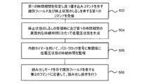
図6は、交換可能な印刷装置構成要素と関連付けられた論理回路(例えば、上述されたような論理回路パッケージ)の動作に関する方法の別の例を示す。この例では、ブロック602において、論理回路は、I2Cデータ・バスを介して、第1の時間期間を指定する第1のコマンドを受信する。この例において、第1のコマンドは、開始(START)状態のしるし、論理回路パッケージのアドレス、書き込みコマンドを示す識別フィールド、及び停止(STOP)状態のしるしも含む(例えば、クロック・パルスの高(HIGH)部分の間にデータ・ライン上の立ち上がる電圧)。
FIG. 6 illustrates another example of a method relating to the operation of logic circuits (eg, logic circuit packages as described above) associated with replaceable printing device components. In this example, at
幾つかの例において、時間期間は、ホスト・デバイスの属性、又はその回路に基づいて選択され得る。一般に、時間期間は、良好なサンプルが捕捉されることを可能にするほど十分に長くなることができるが、交換可能な印刷装置構成要素の位置を検証するのに費やす時間を過度に長くしないぐらいである。 In some examples, the time period may be selected based on attributes of the host device or its circuitry. In general, the time period can be long enough to allow good samples to be captured, but not so long as to unduly lengthen the time spent verifying the position of replaceable printing device components. is.
ブロック604は、論理回路により、停止(STOP)状態(それ自体はコマンドの送信に続く)のしるしの受領後に及び第1の時間期間の実質的な持続時間にわたってI2Cバスのシリアル・データ・ライン上に低電圧状態を生成することを含む。上述されたように、幾つかの例において、低電圧状態は時間期間の全体にわたって生成され得るが、幾つかの例において、方法は、第1の時間期間の一部の間にシリアル・データ・ラインを「フロート高(HIGH)」にすること(即ち、ラインは中断される態様で低に保持され得る)を含むことができる。幾つかの例において、シリアル・データ・ラインは、第1の時間期間の少なくとも60%、又は第1の時間期間の少なくとも70%、又は第1の時間期間の少なくとも80%、又は第1の時間期間の少なくとも90%、又は第1の時間期間の少なくとも95%にわたって、低に保持され得る。幾つかの例において、電圧は、サンプリング期間と確実に一致するのに十分な一部にわたって低に保持される。低電圧状態の持続時間は、少なくとも1つのサンプリング期間を含み、この場合、サンプリングは、上述されたように、印刷装置の処理回路により実行される。更に、データ・ラインが過度に長い時間期間にわたって低に保持される場合、これが通信を阻止するので、これにより、例えばホスト装置は、タイムアウト・エラー又は同類の物を生成することができる。
停止(STOP)状態のしるしの受領後に低電圧状態を生成することは、バスが、データ・パケットの進行している伝送中に阻止されないことを意味する。 Generating a low voltage state after receipt of a STOP condition indication means that the bus is not blocked during ongoing transmission of data packets.
この例において、低電圧状態を生成することは、シリアル・データ・バス上にクロック信号が存在しない状態と一致し、ブロック606は、論理回路の内部タイマーを用いて、低電圧状態の持続時間を監視することを含む。 In this example, generating a low voltage state coincides with the absence of a clock signal on the serial data bus, and block 606 uses an internal timer in the logic circuit to determine the duration of the low voltage state. Including monitoring.
方法は更に、ブロック608において、読み出しモードを示す識別フィールドを有する読み出し要求に応答して、論理回路により、読み出し操作を実行することを含む。言い換えれば、本明細書で説明された特殊機能に加えて、論理回路はI2Cスレーブ・デバイスとして機能することができる。論理回路は、I2Cスレーブ・デバイスの他の特徴、例えば、認証および/または検証の交換に参加すること、読み出し及び/又は書き込みコマンドを受信すること又は読み出し及び/又は書き込みコマンドに作用すること、処理タスクなどを引き受けることなどを呈することができる。
The method further includes, at
図7は、交換可能な印刷装置構成要素と関連する論理回路パッケージ700の一例であり、論理回路パッケージ700は、ロジック(論理回路)702、シリアル・データ・バス・インターフェース704、タイマー706、及びこの例においてメモリ708を含む。論理回路パッケージ700の使用中、ロジック702は、シリアル・データ・バス・インターフェース704に接続されたシリアル・データ・バスを介して論理回路パッケージ700に送信された第1のコマンドに応答し、論理回路パッケージ700はこの例においてシリアル・データ・バス上に低電圧状態を生成するように構成され、タイマー706を用いて時間期間の持続時間を監視する。幾つかの例において、タイマー706は、例えば有線リンク又は無線リンクを介して、ロジック702と通信することができる。幾つかの例において、タイマー706は、ロジック702と共通の基板上に設けられ得る。
FIG. 7 is an example of a
幾つかの例において、ロジック702は、シリアル・データ・バスのクロック信号と無関係に時間期間の持続時間を監視するように構成され得る。シリアル・データ・バス・インターフェース704は、I2Cデータ・バス・インターフェースを含むことができる。
In some examples,
第1のコマンドは、時間期間を指定することができ、ロジック702は、第1の時間期間の実質的な持続時間にわたってシリアル・データ・バス上に低電圧状態を生成するように構成され得る。ロジック702は、上記図4~図6に関連して説明された方法の何らかの態様を実行することができる。
The first command may specify a time period, and
第2のコマンドに応答して、ロジック702は、シリアル・データ・バス・インターフェース704を介して受信したデータをメモリ708に書き込むように構成され得る。読み出し要求に応答して、ロジック702は、メモリ708からデータを読み出して、シリアル・データ・バス・インターフェース704を介してデータ信号を送信するように構成され得る。
In response to the second command,
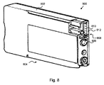
図8は、図7に示されたような論理回路パッケージを含む交換可能な印刷装置構成要素の一例を示す。この例において、交換可能な印刷装置構成要素は、高さより短い幅を有するハウジング802を備える印刷カートリッジ800である。印刷液体出力804(この例において、出口がカートリッジ800の下側に設けられる)、空気入力806、及びリセス808がカートリッジ800の前面に設けられる。リセス808は、カートリッジ800の上部を横切って延び、論理回路パッケージ812(例えば、上述された論理回路パッケージ700)のI2Cバス・コンタクト810が、ハウジング802の上部および前面に隣接してハウジング802の側壁の内壁に対向してリセス808の側面に設けられる。この例において、論理回路パッケージ812は、側壁の内側に当接して設けられる。
FIG. 8 shows an example of a replaceable printing device component that includes a logic circuit package such as that shown in FIG. In this example, the replaceable printing device component is a
本開示の例は、ソフトウェア、ハードウェア、ファームウェア又は同類の物の任意の組み合わせのような、方法、システム又は機械可読命令として提供され得る。係る機械可読命令は、機械可読記憶媒体(以下に限定されないが、ディスク記憶装置、CD-ROM、光学式記憶措置などを含む)に含まれることができ、当該機械可読記憶媒体は、その中に又はその上に機械可読プログラム・コードを有する。 Examples of the present disclosure may be provided as a method, system or machine readable instructions, such as any combination of software, hardware, firmware or the like. Such machine-readable instructions may be contained on a machine-readable storage medium (including, but not limited to, disk storage devices, CD-ROMs, optical storage devices, etc.), in which or have machine-readable program code thereon.
本開示は、本開示の例による、方法、デバイス及びシステムの流れ図およびブロック図に関連して説明される。上述された流れ図は実行の特定の順序を示すが、実行の順序は、示された順序と異なることができる。1つの流れ図に関連して記載されたブロックは、別の流れ図のブロックと組み合わされ得る。理解されるべきは、流れ図およびブロック図、並びにそれらの組みあわせの少なくとも幾つかのブロックは、機械可読命令により実現され得る。 The present disclosure is described with reference to flowchart illustrations and block diagrams of methods, devices and systems according to examples of the disclosure. Although the flow diagrams described above show a particular order of execution, the order of execution can differ from that shown. Blocks described in association with one flowchart may be combined with blocks of another flowchart. It should be understood that at least some of the blocks in the flow diagrams and block diagrams, and combinations thereof, can be implemented by machine readable instructions.
機械可読命令は例えば、汎用コンピュータ、専用コンピュータ、説明および図面に記載された機能を実現するための他のプログラム可能なデータ処理デバイスの組み込みプロセッサ又はプロセッサにより、実行され得る。特に、プロセッサ又は処理回路は、機械可読命令を実行することができる。かくして、装置およびデバイスの機能モジュール(例えば、論理回路および/またはコントローラ)は、メモリに格納された機械可読命令を実行するプロセッサにより、又は論理回路に埋め込まれた命令に従って動作するプロセッサにより、具現化され得る。用語「プロセッサ」は、CPU、処理ユニット、ASIC、論理ユニット又はプログラム可能ゲート・アレイなどを含むように広く解釈されるべきである。方法および機能モジュールは全て、単一のプロセッサによって実行され得る、又は幾つかのプロセッサ間で分担され得る。 Machine-readable instructions can be executed, for example, by an embedded processor or processor of a general purpose computer, special purpose computer, or other programmable data processing device to perform the functions described in the description and drawings. In particular, a processor or processing circuit is capable of executing machine-readable instructions. Thus, functional modules (e.g., logic circuits and/or controllers) of apparatus and devices are embodied by processors executing machine-readable instructions stored in memory or by processors operating according to instructions embedded in logic circuits. can be The term "processor" should be interpreted broadly to include CPUs, processing units, ASICs, logic units or programmable gate arrays, and the like. All methods and functional modules may be executed by a single processor or may be shared among several processors.
また、係る機械可読命令は、機械可読記憶装置(例えば、有形の機械可読媒体)に格納されることもでき、特定のモードで動作するためにコンピュータ又は他のプログラム可能データ処理デバイスを案内することができる。 Such machine-readable instructions may also be stored on a machine-readable storage device (e.g., a tangible machine-readable medium) to guide a computer or other programmable data processing device to operate in a particular mode. can be done.
また、係る機械可読命令は、コンピュータ又は他のプログラム可能データ処理装置上へロードされることができ、そのため、コンピュータ又は他のプログラム可能データ処理装置は、コンピュータにより実現される処理を生成するために一連の演算を実行し、かくして、コンピュータ又は他のプログラム可能データ処理装置上で実行された命令は、流れ図および/またはブロック図のブロック(単数または複数)により指定された機能を実現する。 Also, such machine-readable instructions can be loaded onto a computer or other programmable data processing apparatus such that the computer or other programmable data processing apparatus can be used to generate computer-implemented processes. The instructions executed on the computer or other programmable data processing apparatus perform the sequences of operations and thus perform the functions specified by the block(s) in the flow diagrams and/or block diagrams.
更に、本明細書の教示は、コンピュータ・ソフトウェア製品の形態で具現化されることができ、当該コンピュータ・ソフトウェア製品は、記憶媒体に格納され、本開示の例に記載された方法をコンピュータ・デバイスに具現化させるための複数の命令を含む。 Furthermore, the teachings herein can be embodied in the form of a computer software product stored on a storage medium and used to implement the methods described in the examples of this disclosure on a computer device. contains a number of instructions for implementing the
方法、装置および関連した態様は特定の例に関連して説明されたが、様々な変形、変更、省略、及び置換は、本開示の精神から逸脱せずに行われ得る。従って、方法、装置および関連した態様は、以下の特許請求の範囲およびそれらの等価物の範囲によってのみ制限されることが意図されている。留意されるべきは、上述した例は、本明細書で説明されたことを制限するために示したのではなく、当業者は添付の特許請求の範囲から逸脱せずに多くの代替の具現化形態を設計することができる。一例に関連して説明された特徴は、別の例の特徴と組み合わされ得る。 Although the methods, apparatus, and related aspects have been described with reference to particular examples, various modifications, alterations, omissions, and substitutions may be made without departing from the spirit of the disclosure. It is therefore intended that the methods, apparatus and related aspects be limited only by the scope of the following claims and their equivalents. It should be noted that the examples described above are not meant to limit what has been described herein, but that those skilled in the art will be able to make many alternative implementations without departing from the scope of the appended claims. You can design the form. Features described in relation to one example may be combined with features of another example.
用語「含む」は、特許請求の範囲に列挙されたもの以外の要素の存在を排除せず、「a」又は「an」は複数を除外せず、単一のプロセッサ又は他のユニットは、特許請求の範囲に記載された幾つかのユニットの機能を実現することができる。 The word "comprising" does not exclude the presence of elements other than those listed in a claim, nor does "a" or "an" exclude a plurality; The functions of several units recited in the claims may be implemented.
任意の従属請求項の特徴は、独立請求項または他の従属請求項の何れかの特徴と組み合わされ得る。 Features of any dependent claim may be combined with features of any independent or other dependent claim.
ステートメント
幾つかの例において、方法は、以下のステートメントの何れかにより説明され得る。
ステートメント1.
シリアル・データ・バスを介して、交換可能な印刷装置構成要素と関連付けられた論理回路のアドレスに送信された第1のコマンドに応答して、
前記論理回路により、前記シリアル・データ・バス上に低電圧状態を生成し、
前記論理回路のタイマーを用いて、前記低電圧状態の持続時間を監視することを含む、方法。
ステートメント2.前記第1のコマンドが第1の時間期間を指定し、前記シリアル・データ・バス上に低電圧状態を生成することは、前記第1の時間期間に基づいて前記シリアル・データ・バス上に低電圧状態を生成することを含む、ステートメント1に記載の方法。
ステートメント3.前記第1の時間期間の実質的な持続時間にわたって、前記シリアル・データ・バス上に低電圧状態を生成することを含む、ステートメント2に記載の方法。
ステートメント4.前記シリアル・データ・バスのシリアル・データ・ライン上に低電圧状態を生成することを含む、ステートメント1~3の何れか1項に記載の方法。
ステートメント5.前記低電圧状態の持続時間は、少なくとも1つのサンプリング期間を含み、サンプリングが前記サンプリング期間の間に印刷装置の処理回路により実行される、ステートメント1~4の何れか1項に記載の方法。
ステートメント6.前記低電圧状態を生成することは、前記シリアル・データ・バス上にクロック信号がない状態と一致する、ステートメント1~5の何れか1項に記載の方法。
ステートメント7.前記第1のコマンドは、書き込みコマンドを示す識別フィールド、及び停止状態のしるしを含み、
方法は、前記論理回路により、前記停止状態のしるしの受領後に前記シリアル・データ・バス上に低電圧状態を生成することを更に含む、ステートメント1~6の何れか1項に記載の方法。
ステートメント8.読み出しモードを示す識別フィールドを有する読み出し要求に応答して、前記論理回路により、読み出し操作を行うことを更に含む、ステートメント7に記載の方法。
ステートメント9.前記低電圧状態の電圧値は、前記印刷装置における前記交換可能な印刷装置構成要素の位置を示す、ステートメント1~8の何れか1項に記載の方法。
ステートメント10.前記シリアル・データ・バスが異なる高および/またはデフォルトの電圧状態または電圧状況になるように、前記低電圧状態を解除することを更に含む、ステートメント1~9の何れか1項に記載の方法。
ステートメント11.交換可能な印刷装置構成要素と関連する論理回路パッケージであって、
ロジック及びシリアル・データ・バス・インターフェースを含み、
前記シリアル・データ・バス・インターフェースは、印刷装置のシリアル・データ・バスと接続して機能することができ、
前記ロジックは、前記シリアル・データ・バス・インターフェースに接続された前記シリアル・データ・バスを介して前記論理回路パッケージに送信された第1のコマンドに応答して、前記シリアル・データ・バス上に低電圧状態を生成して、時間期間の持続時間を監視することができる、論理回路パッケージ。
ステートメント12.タイマーを更に含み、前記ロジックは、前記タイマーを用いて前記時間期間の持続時間を監視することができる、ステートメント11に記載の論理回路パッケージ。
ステートメント13.前記ロジックは、前記時間期間の終わりで前記シリアル・データ・バス上の前記低電圧状態を解除することができる、ステートメント11又は12に記載の論理回路パッケージ。
ステートメント14.前記ロジックは、前記時間期間外で、前記シリアル・データ・バスを異なる高および/またはデフォルトの電圧状態または電圧状況にするように構成されている、ステートメント11~13の何れか1項に記載の論理回路パッケージ。
ステートメント15.前記ロジックは、前記第1のコマンドを受信した際に前記低電圧状態を生成する前に、確認応答を出力することができる、ステートメント11~14の何れか1項に記載の論理回路パッケージ。
ステートメント16.前記ロジックは、前記シリアル・データ・バスのクロック信号に無関係に前記時間期間の持続時間を監視することができる、ステートメント11~15の何れか1項に記載の論理回路パッケージ。
ステートメント17.前記第1のコマンドは時間期間を指定し、前記ロジックは、前記時間期間の持続時間内で前記シリアル・データ・バス上に低電圧状態を生成することができる、ステートメント11~16の何れか1項に記載の論理回路パッケージ。
ステートメント18.前記ロジックは、前記第1のコマンドに指定された前記時間期間にわたって前記低電圧状態を生成するように構成される、ステートメント11~17の何れか1項に記載の論理回路パッケージ。
ステートメント19.前記第1のコマンドは、時間期間を指定し、前記ロジックは、前記時間期間の実質的な持続時間にわたって前記シリアル・データ・バス上に低電圧状態を生成することができる、ステートメント11~18の何れか1項に記載の論理回路パッケージ。
ステートメント20.メモリを更に含み、第2のコマンドに応答して、前記ロジックは、前記シリアル・データ・バス・インターフェースを介して受信したデータを前記メモリに書き込むことができる、ステートメント11~19の何れか1項に記載の論理回路パッケージ。
ステートメント21.メモリを更に含み、読み出し要求に応答して、前記ロジックは、前記メモリからデータを読み出して、前記シリアル・データ・バス・インターフェースを介してデータ信号を送信することができる、ステートメント11~20の何れか1項に記載の論理回路パッケージ。
ステートメント22.前記シリアル・データ・バス・インターフェースがI2Cデータ・バス・インターフェースである、ステートメント11~21の何れか1項に記載の論理回路パッケージ。
ステートメント23.2つ以上のI2Cアドレスを介して、同じI2Cバス・インターフェースにわたって通信し、
異なる二次I2Cアドレスを一時的に用いて、第2の時間期間を含むコマンドと関連付けられたコマンドを受信し、
前記第2の時間期間を監視し、
前記第2の時間期間中に前記二次I2Cアドレスに向けられたコマンドに応答するように構成されている、ステートメント11~22の何れか1項に記載の論理回路パッケージ。
ステートメント24.前記論理回路パッケージは、タイマーを含み、前記第2の時間期間が前記タイマーを用いて監視される、ステートメント12に従属するステートメント22に記載の論理回路パッケージ。
ステートメント25.ステートメント11~24の何れか1項に記載の論理回路パッケージを含む、交換可能な印刷装置構成要素。
ステートメント26.印刷装置に接続するための交換可能な印刷装置カートリッジであって、
着色された印刷材料を含むリザーバと、
論理回路パッケージとを含み、
前記論理回路パッケージは、
ロジック及びシリアル・データ・バス・インターフェースを含み、
前記シリアル・データ・バス・インターフェースは、印刷装置のシリアル・データ・バスに接続されることができ、
前記ロジックは、前記印刷装置に接続された際に前記交換可能な印刷装置カートリッジの場所を求めるために、前記シリアル・データ・バス・インターフェースに接続されたシリアル・データ・バスを介して前記論理回路パッケージに送信された第1のコマンドに応答して、前記シリアル・データ・バス上に低電圧状態を生成し、時間期間の持続時間を監視することができる、交換可能な印刷装置カートリッジ。
ステートメント27.ステートメント11~25の何れか1項に記載された特徴の何れかを更に含む、ステートメント26に記載の交換可能な印刷装置カートリッジ。
ステートメント28.内部にはしご型抵抗回路網を有する通信バスを含み、ステートメント11~25の何れか1項に記載された論理回路パッケージの少なくとも2つを受容するように適合された印刷装置であって、前記論理回路パッケージは異なるI2Cアドレスを有し、各論理回路パッケージは、前記はしご型抵抗回路網の異なる箇所で前記通信バスに接続されて、所定のコマンドに応答して前記通信バス上に異なる低電圧状態を生成する、印刷装置。
Statements In some examples, a method can be described by any of the following statements.
Statement 1.
in response to a first command sent over the serial data bus to an address of a logic circuit associated with a replaceable printing device component;
generating a low voltage state on the serial data bus with the logic circuit;
A method comprising monitoring the duration of the low voltage condition using a timer of the logic circuit.
Statement 2. The first command specifies a first time period and generating a low voltage state on the serial data bus causes a low voltage state on the serial data bus based on the first time period. The method of Statement 1 including generating the voltage state.
Statement 3. 3. The method of statement 2 including generating a low voltage state on said serial data bus for a substantial duration of said first time period.
Statement 4. 4. The method of any one of statements 1-3, including generating a low voltage state on a serial data line of the serial data bus.
Statement 5. 5. The method of any one of statements 1-4, wherein the duration of the low voltage state includes at least one sampling period, and sampling is performed by processing circuitry of the printing device during the sampling period.
Statement 6. 6. The method of any one of statements 1-5, wherein generating the low voltage condition coincides with no clock signal on the serial data bus.
Statement 7. the first command includes an identification field indicating a write command and an indicia of a halt condition;
7. The method of any one of statements 1-6, further comprising generating, by the logic circuit, a low voltage state on the serial data bus after receiving the indication of the halt condition.
Statement 8. 8. The method of Statement 7, further comprising performing a read operation with the logic circuit in response to a read request having an identification field indicating a read mode.
Statement 9. 9. The method of any one of statements 1-8, wherein the voltage value of the low voltage state indicates a position of the replaceable printing device component in the printing device.
Statement 10. 10. The method of any one of statements 1-9, further comprising releasing the low voltage state such that the serial data bus is in a different high and/or default voltage state or voltage condition.
Statement 11. A logic circuit package associated with a replaceable printing device component, comprising:
including logic and serial data bus interfaces;
the serial data bus interface is operable in connection with a serial data bus of a printing device;
on the serial data bus in response to a first command sent to the logic circuit package via the serial data bus connected to the serial data bus interface; A logic circuit package capable of generating a low voltage state and monitoring the duration of a time period.
Statement 12. 12. The logic circuit package of statement 11, further comprising a timer, wherein the logic can monitor the duration of the time period using the timer.
Statement 13. 13. The logic circuit package of statement 11 or 12, wherein said logic is capable of releasing said low voltage condition on said serial data bus at the end of said time period.
Statement 14. 14. The statement of any one of statements 11-13, wherein the logic is configured to put the serial data bus into different high and/or default voltage states or conditions outside of the time period. Logic circuit package.
Statement 15. 15. The logic circuit package of any one of statements 11-14, wherein the logic is capable of outputting an acknowledgment prior to generating the low voltage state upon receiving the first command.
Statement 16. 16. The logic circuit package of any one of statements 11-15, wherein the logic is capable of monitoring the duration of the time period independently of a clock signal on the serial data bus.
Statement 17. any one of statements 11-16, wherein the first command specifies a time period and the logic is capable of generating a low voltage state on the serial data bus within the duration of the time period Logic circuit package as described above.
Statement 18. 18. The logic circuit package of any one of statements 11-17, wherein the logic is configured to generate the low voltage state for the period of time specified in the first command.
Statement 19. of statements 11-18, wherein the first command specifies a time period and the logic can generate a low voltage state on the serial data bus for a substantial duration of the time period; A logic circuit package according to any one of claims 1 to 3.
Statement 20. 20. Any one of statements 11-19, further comprising a memory, and in response to a second command, the logic being capable of writing data received via the serial data bus interface to the memory. logic circuit package described in .
Statement 21. 21. Any of statements 11-20, further comprising a memory, and in response to a read request, the logic can read data from the memory and transmit data signals over the serial data bus interface. 2. A logic circuit package according to claim 1.
Statement 22. 22. The logic circuit package of any one of statements 11-21, wherein the serial data bus interface is an I2C data bus interface.
Statement 23. Communicate over the same I2C bus interface via two or more I2C addresses;
temporarily using a different secondary I2C address to receive a command associated with the command including the second time period;
monitor the second time period;
23. The logic circuit package of any one of statements 11-22, configured to respond to commands directed to the secondary I2C address during the second time period.
Statement 24. 22. Dependent from statement 12, the logic circuit package of statement 22, wherein the logic circuit package includes a timer, and wherein the second period of time is monitored using the timer.
Statement 25. A replaceable printing device component comprising a logic circuit package according to any one of statements 11-24.
Statement 26. A replaceable printing device cartridge for connection to a printing device, comprising:
a reservoir containing pigmented printing material;
a logic circuit package;
The logic circuit package includes:
including logic and serial data bus interfaces;
the serial data bus interface can be connected to a serial data bus of a printing device;
The logic communicates the logic circuit via a serial data bus connected to the serial data bus interface to determine the location of the replaceable printing device cartridge when connected to the printing device. A replaceable printer cartridge capable of producing a low voltage state on said serial data bus and monitoring the duration of a time period in response to a first command sent to the package.
Statement 27. 26. The replaceable printer cartridge of Statement 26, further including any of the features of any one of Statements 11-25.
Statement 28. 26. A printing device including a communication bus having a resistive ladder network therein and adapted to receive at least two of the logic circuit packages of any one of statements 11-25, wherein said logic The circuit packages have different I2C addresses and each logic circuit package is connected to the communication bus at a different point of the ladder resistor network to produce a different low voltage state on the communication bus in response to a predetermined command. A printing device that produces
Claims (22)
前記論理回路により、前記第1の時間期間に基づいて設定された持続時間にわたって前記シリアル・データ・バス上に低電圧状態を生成し、
前記シリアル・データ・バスのクロック信号と無関係に、前記論理回路のタイマーを用いて、前記低電圧状態の持続時間を監視し、
前記第1の時間期間に基づいて設定された持続時間外で、前記シリアル・データ・バスが高および/またはデフォルトの異なる電圧状態または電圧状況になるように、前記低電圧状態を解除することを含む、方法。 in response to a first command specifying a first period of time sent over the serial data bus to an address of a logic circuit associated with a replaceable printing device component;
causing the logic circuit to generate a low voltage state on the serial data bus for a duration set based on the first time period;
monitoring the duration of the low voltage state using a timer of the logic circuit independently of the serial data bus clock signal;
releasing the low voltage state such that the serial data bus is in a high and/or default different voltage state or voltage condition outside of the duration set based on the first time period; including, method.
方法は、前記論理回路により、前記停止状態のしるしの受領後に前記シリアル・データ・バス上に低電圧状態を生成することを更に含む、請求項1~5の何れか1項に記載の方法。 the first command includes an identification field indicating a write command and an indicia of a halt condition;
A method according to any one of claims 1 to 5, further comprising generating, by said logic circuit, a low voltage state on said serial data bus after receiving said indication of a halt condition.
ロジック、タイマー及びシリアル・データ・バス・インターフェースを含み、
前記シリアル・データ・バス・インターフェースは、印刷装置のシリアル・データ・バスと接続して機能することができ、
前記ロジックは、前記シリアル・データ・バス・インターフェースに接続された前記シリアル・データ・バスを介して前記論理回路パッケージの第1のアドレスに送信された、第1の時間期間を指定する第1のコマンドに応答して、
前記第1の時間期間に基づいて設定された持続時間にわたって、前記シリアル・データ・バス上に低電圧状態を生成し、
前記シリアル・データ・バスのクロック信号と無関係に、前記タイマーを用いて前記第1の時間期間に基づいて設定された持続時間を監視し、
前記第1の時間期間に基づいて設定された持続時間外で、前記シリアル・データ・バスを高および/またはデフォルトの異なる電圧状態または電圧状況にすることができる、論理回路パッケージ。 A logic circuit package associated with a replaceable printing device component, comprising:
including logic, timer and serial data bus interface;
the serial data bus interface is operable in connection with a serial data bus of a printing device;
The logic includes a first address specifying a first time period sent to a first address of the logic circuit package over the serial data bus connected to the serial data bus interface. in response to the command
generating a low voltage state on the serial data bus for a duration set based on the first time period;
using the timer to monitor a duration set based on the first time period, independently of the clock signal on the serial data bus;
A logic circuit package capable of driving the serial data bus to high and/or default different voltage states or conditions outside of the duration set based on the first time period.
クロック周波数より速く計数し、且つ
クロック信号のタイミングに関係無く計数することを開始および停止するように構成される、請求項9に記載の論理回路パッケージ。 The timer
10. The logic circuit package of claim 9, configured to count faster than a clock frequency and to start and stop counting regardless of the timing of the clock signal.
異なる二次I2Cアドレスを一時的に用いて、第2の時間期間を含むコマンドと関連付けられたコマンドを受信し、
前記第2の時間期間を監視し、
前記第2の時間期間中に前記二次I2Cアドレスに向けられたコマンドに応答するように構成されている、請求項18に記載の論理回路パッケージ。 communicate over the same I2C bus interface via two or more I2C addresses;
temporarily using a different secondary I2C address to receive a command associated with the command including the second time period;
monitor the second time period;
19. The logic circuit package of claim 18, configured to respond to commands directed to said secondary I2C address during said second time period.
着色された印刷材料を含むリザーバと、
請求項9~20の何れか1項に記載の論理回路パッケージとを含み、前記交換可能な印刷装置カートリッジは、請求項9~20の何れか1項に記載の前記交換可能な印刷装置構成要素である、印刷装置カートリッジ。 A replaceable printing device cartridge for connection to a printing device, comprising:
a reservoir containing pigmented printing material;
and a logic circuit package according to any one of claims 9 to 20, wherein said replaceable printing device cartridge is said replaceable printing device component according to any one of claims 9 to 20. , a printer cartridge.
Applications Claiming Priority (1)
| Application Number | Priority Date | Filing Date | Title |
|---|---|---|---|
| PCT/US2018/063633 WO2020117196A1 (en) | 2018-12-03 | 2018-12-03 | Logic circuitry |
Publications (2)
| Publication Number | Publication Date |
|---|---|
| JP2022511652A JP2022511652A (en) | 2022-02-01 |
| JP7200370B2 true JP7200370B2 (en) | 2023-01-06 |
Family
ID=64734242
Family Applications (2)
| Application Number | Title | Priority Date | Filing Date |
|---|---|---|---|
| JP2021523069A Active JP7200370B2 (en) | 2018-12-03 | 2018-12-03 | logic circuit |
| JP2021529280A Active JP7011102B2 (en) | 2018-12-03 | 2019-02-11 | Logic circuit |
Family Applications After (1)
| Application Number | Title | Priority Date | Filing Date |
|---|---|---|---|
| JP2021529280A Active JP7011102B2 (en) | 2018-12-03 | 2019-02-11 | Logic circuit |
Country Status (21)
| Country | Link |
|---|---|
| US (5) | US11256654B2 (en) |
| EP (4) | EP3767480B1 (en) |
| JP (2) | JP7200370B2 (en) |
| KR (2) | KR20210087064A (en) |
| CN (6) | CN111880387B (en) |
| AR (2) | AR117240A1 (en) |
| AU (2) | AU2018452006B2 (en) |
| BR (1) | BR112021010792A2 (en) |
| CA (2) | CA3114001C (en) |
| CL (2) | CL2021001189A1 (en) |
| DK (4) | DK3688601T3 (en) |
| ES (4) | ES2830401T3 (en) |
| IL (1) | IL281933B2 (en) |
| MX (2) | MX2021005849A (en) |
| MY (1) | MY190371A (en) |
| NZ (1) | NZ776685A (en) |
| PL (2) | PL3767480T3 (en) |
| PT (3) | PT3688601T (en) |
| TW (2) | TWI737047B (en) |
| WO (2) | WO2020117196A1 (en) |
| ZA (1) | ZA202101623B (en) |
Families Citing this family (5)
| Publication number | Priority date | Publication date | Assignee | Title |
|---|---|---|---|---|
| DE102017215528A1 (en) | 2017-09-05 | 2019-03-07 | Sarstedt Ag & Co. Kg | Napf or Napfstreifen and process for its preparation |
| DK3688601T3 (en) | 2018-12-03 | 2020-11-16 | Hewlett Packard Development Co | LOGICAL CIRCUIT |
| WO2022086538A1 (en) | 2020-10-22 | 2022-04-28 | Hewlett-Packard Development Company, L.P. | Logic circuitry |
| US11934285B2 (en) * | 2021-01-15 | 2024-03-19 | Google Llc | Identification/communication interface between consumer electronic devices and accessory devices |
| TWI795884B (en) * | 2021-08-25 | 2023-03-11 | 立積電子股份有限公司 | Device of measuring duty cycle and compensation circuit |
Citations (3)
| Publication number | Priority date | Publication date | Assignee | Title |
|---|---|---|---|---|
| JP2011168004A (en) | 2010-02-22 | 2011-09-01 | Seiko Epson Corp | Memory device, substrate, liquid vessel, host device, and system |
| JP2011525004A (en) | 2008-05-21 | 2011-09-08 | ヒューレット−パッカード デベロップメント カンパニー エル.ピー. | Multi-drop serial bus and method having position detection function |
| JP2018116423A (en) | 2017-01-17 | 2018-07-26 | キヤノン株式会社 | Image processing device |
Family Cites Families (151)
| Publication number | Priority date | Publication date | Assignee | Title |
|---|---|---|---|---|
| US4506276A (en) | 1977-06-16 | 1985-03-19 | System Industries, Inc. | Ink supply system |
| US4639738A (en) | 1985-04-12 | 1987-01-27 | Eastman Kodak Company | Ink level detection system for ink jet printing apparatus |
| US5142909A (en) | 1986-09-29 | 1992-09-01 | Baughman James S | Material level indicator |
| US5001596A (en) | 1990-05-07 | 1991-03-19 | Therm-O-Disc, Incorporated | Capacitive fluid level sensor |
| JPH05289778A (en) * | 1992-04-10 | 1993-11-05 | Fuji Xerox Co Ltd | Information processor |
| US5680960A (en) | 1993-03-05 | 1997-10-28 | Keyes; Denis E. | Volumetric fluid dispensing apparatus |
| JP3428191B2 (en) * | 1994-12-26 | 2003-07-22 | 株式会社デンソー | Data communication method, transmitting device, and receiving device |
| JPH0939265A (en) | 1995-07-29 | 1997-02-10 | Seiko Epson Corp | Ink cartridge for printer and identifying device therefor |
| WO1998055318A1 (en) | 1997-06-04 | 1998-12-10 | Hewlett-Packard Company | Ink delivery system adapter |
| US5964718A (en) | 1997-11-21 | 1999-10-12 | Mercury Diagnostics, Inc. | Body fluid sampling device |
| US6089687A (en) | 1998-03-09 | 2000-07-18 | Hewlett-Packard Company | Method and apparatus for specifying ink volume in an ink container |
| US6151041A (en) | 1998-10-19 | 2000-11-21 | Lexmark International, Inc. | Less restrictive print head cartridge installation in an ink jet printer |
| US6981215B1 (en) | 1998-12-31 | 2005-12-27 | Microsoft Corp. | System for converting event-driven code into serially executed code |
| US6098457A (en) | 1999-01-18 | 2000-08-08 | Cts Corporation | Fluid level detector using thermoresistive sensor |
| US6729707B2 (en) | 2002-04-30 | 2004-05-04 | Hewlett-Packard Development Company, L.P. | Self-calibration of power delivery control to firing resistors |
| GB9920301D0 (en) | 1999-08-27 | 1999-11-03 | Philipp Harald | Level sensing |
| US6190000B1 (en) * | 1999-08-30 | 2001-02-20 | Hewlett-Packard Company | Method and apparatus for masking address out failures |
| MY127696A (en) | 2000-05-18 | 2006-12-29 | Seiko Epson Corp | Method and apparatus for detecting consumption of ink |
| DE60135064D1 (en) | 2000-06-16 | 2008-09-11 | Canon Kk | An ink jet recording apparatus using a solid state semiconductor device |
| US6378977B1 (en) * | 2000-06-30 | 2002-04-30 | Hewlett-Packard Company | System and method for conveying printer status information |
| WO2002002227A2 (en) | 2000-07-03 | 2002-01-10 | Xeotron Corporation | Devices and methods for carrying out chemical reactions using photogenerated reagents |
| GB0020268D0 (en) | 2000-08-18 | 2000-10-04 | Neopost Ltd | Control of quality of printing |
| TW505572B (en) | 2000-10-20 | 2002-10-11 | Internat United Technoloy Co L | Ink container with pressure regulation device |
| TW503186B (en) | 2001-02-02 | 2002-09-21 | Benq Corp | Detecting device for ink storage |
| CA2371040A1 (en) | 2001-02-09 | 2002-08-09 | Nobuyuki Hatasa | Liquid container and recording apparatus |
| US6648434B2 (en) | 2001-03-08 | 2003-11-18 | Hewlett-Packard Development Company, L.P. | Digitally compensated pressure ink level sense system and method |
| US6546796B2 (en) | 2001-03-15 | 2003-04-15 | Therm-O-Disc, Incorporated | Liquid level sensor |
| US6456802B1 (en) | 2001-04-02 | 2002-09-24 | Hewlett-Packard Co. | Capacity determination for toner or ink cartridge |
| US20030009595A1 (en) | 2001-07-09 | 2003-01-09 | Roger Collins | System and method for compressing data using field-based code word generation |
| US6802581B2 (en) | 2002-07-30 | 2004-10-12 | Hewlett-Packard Development Company, L.P. | Method, program product and system for ink management control |
| US7077506B2 (en) | 2002-08-01 | 2006-07-18 | Benq Corporation | Identifiable inkjet cartridge and method of preventing misplacing inkjet cartridge in an inkjet apparatus |
| EP1389531B1 (en) | 2002-08-12 | 2007-07-18 | Seiko Epson Corporation | Container for printing material, technique of detecting information on printing material in container, and technique of allowing for transmission of information between container and printing device |
| US7201463B2 (en) | 2002-08-12 | 2007-04-10 | Seiko Epson Corporation | Container for printing material and detector used for container |
| US7529868B2 (en) | 2002-12-20 | 2009-05-05 | Transact Technologies Incorporated | Method and apparatus for controlling a peripheral via different data ports |
| CN2603934Y (en) | 2003-01-16 | 2004-02-18 | 杨伟雄 | Electronic spring balance |
| US6685290B1 (en) | 2003-01-30 | 2004-02-03 | Hewlett-Packard Development Company, L.P. | Printer consumable having data storage for static and dynamic calibration data, and methods |
| JP2004266783A (en) | 2003-02-04 | 2004-09-24 | Vanfu Inc | Color matching method in preparation of printing color image |
| US6959599B2 (en) | 2003-04-10 | 2005-11-01 | Robert Feldstein | Level detector for storage tanks for fluids |
| US6926397B2 (en) | 2003-04-29 | 2005-08-09 | Hewlett-Packard Development Company, L.P. | Cartridge tape removal apparatus and method |
| US6796644B1 (en) | 2003-06-18 | 2004-09-28 | Lexmark International, Inc. | Ink source regulator for an inkjet printer |
| US7101029B2 (en) * | 2003-10-31 | 2006-09-05 | Hewlett-Packard Development Company, L.P. | Interconnect circuit |
| US6966222B2 (en) | 2003-12-08 | 2005-11-22 | Hewlett-Packard Development Company, L.P. | Methods and apparatus for media level measurement |
| US20050126282A1 (en) | 2003-12-16 | 2005-06-16 | Josef Maatuk | Liquid sensor and ice detector |
| KR20050098142A (en) * | 2004-04-06 | 2005-10-11 | 삼성전자주식회사 | Electronic device for communicating with host through serial communication interface |
| US7107838B2 (en) | 2004-04-19 | 2006-09-19 | Fook Tin Technologies Ltd. | Apparatus and methods for monitoring water consumption and filter usage |
| US7775105B2 (en) | 2004-04-21 | 2010-08-17 | Therm-O-Disc, Incorporated | Multi-function sensor |
| CN1287259C (en) * | 2004-05-19 | 2006-11-29 | 中兴通讯股份有限公司 | Device and method for operating multiple I2C sub device in communication equipment |
| US7093989B2 (en) | 2004-05-27 | 2006-08-22 | Silverbrook Research Pty Ltd | Printer comprising two uneven printhead modules and at least two printer controllers, one which spends print data to the other |
| JP4525212B2 (en) | 2004-07-07 | 2010-08-18 | 船井電機株式会社 | Thermal transfer printer |
| JP2006099410A (en) | 2004-09-29 | 2006-04-13 | Mitsubishi Electric Corp | Method for controlling i2c |
| JP4047328B2 (en) | 2004-12-24 | 2008-02-13 | キヤノン株式会社 | Liquid storage container, liquid supply system and recording apparatus using the container, and circuit board for the container |
| US7610526B2 (en) * | 2005-01-24 | 2009-10-27 | Hewlett-Packard Development Company, L.P. | On-chip circuitry for bus validation |
| JP2006224395A (en) | 2005-02-16 | 2006-08-31 | Seiko Epson Corp | Method for controlling functional liquid feeding apparatus, functional liquid feeding apparatus, liquid droplet delivering apparatus, method for manufacturing electrooptic apparatus, electrooptic apparatus and electronic instrument |
| FR2885710B1 (en) | 2005-05-11 | 2007-08-03 | Stmicroelectronics Maroc | ADDRESS SELECTION FOR I2C BUS |
| KR100694134B1 (en) | 2005-07-05 | 2007-03-12 | 삼성전자주식회사 | Ink cartridge including a means for sensing the amount of residual ink |
| JP2007018288A (en) | 2005-07-07 | 2007-01-25 | Fuji Xerox Co Ltd | Arithmetic processor and power saving mode changeover method therefor |
| KR20070059247A (en) * | 2005-12-06 | 2007-06-12 | 삼성전자주식회사 | Apparatus and method for serial bus interfacing between printed circuit board assemblies |
| US7444453B2 (en) * | 2006-01-03 | 2008-10-28 | International Business Machines Corporation | Address translation device |
| KR100772389B1 (en) * | 2006-01-12 | 2007-11-01 | 삼성전자주식회사 | Apparatus for cognizing memory |
| US8562645B2 (en) | 2006-09-29 | 2013-10-22 | Biomet Sports Medicine, Llc | Method and apparatus for forming a self-locking adjustable loop |
| JP2008030219A (en) | 2006-07-26 | 2008-02-14 | Seiko Epson Corp | Liquid jet system, liquid container, and method for judging residual amount of liquid in liquid container |
| WO2008058335A1 (en) | 2006-11-15 | 2008-05-22 | Depth Analysis Pty Ltd | Systems and methods for managing the production of a free-viewpoint video-based animation |
| US20080246626A1 (en) | 2007-04-03 | 2008-10-09 | Vizionware, Inc. | Data transaction direction detection in an adaptive two-wire bus |
| US20080307134A1 (en) | 2007-06-05 | 2008-12-11 | Geissler Andrew J | I2C bus interface and protocol for thermal and power management support |
| JP2009023187A (en) | 2007-07-19 | 2009-02-05 | Citizen Holdings Co Ltd | Print system |
| US8128186B2 (en) * | 2007-07-27 | 2012-03-06 | Hewlett-Packard Development Company, L.P. | Non-volatile memory data integrity validation |
| GB0720289D0 (en) * | 2007-10-12 | 2007-11-28 | Videojet Technologies Inc | Ink jet printer |
| EP2280756B1 (en) | 2008-04-29 | 2014-07-23 | St. Jude Medical AB | An implantable medical lead and a method of manufacturing thereof |
| CN105701058B (en) * | 2008-05-21 | 2019-05-03 | 惠普开发有限公司 | Multi-drop serial bus and method with position detection |
| HUE046819T2 (en) | 2008-05-29 | 2020-03-30 | Hewlett Packard Development Co | Authenticating a replaceable printer component |
| ATE543139T1 (en) | 2008-07-16 | 2012-02-15 | St Microelectronics Rousset | INTERFACE BETWEEN A DUAL LINE BUS AND A SINGLE LINE BUS |
| JP2010208288A (en) * | 2009-03-12 | 2010-09-24 | Ricoh Co Ltd | Image formation apparatus |
| JP5478101B2 (en) | 2009-03-31 | 2014-04-23 | シスメックス株式会社 | Reagent preparation apparatus and specimen processing system |
| US8289788B2 (en) * | 2009-04-01 | 2012-10-16 | Seiko Epson Corporation | System having a plurality of memory devices and data transfer method for the same |
| JP5257236B2 (en) | 2009-05-20 | 2013-08-07 | 株式会社リコー | Image forming medium container, ink cartridge, and image forming apparatus |
| US8225021B2 (en) | 2009-05-28 | 2012-07-17 | Lexmark International, Inc. | Dynamic address change for slave devices on a shared bus |
| US8621116B2 (en) | 2011-08-26 | 2013-12-31 | Lexmark International, Inc. | Dynamic address change optimizations |
| JP5515523B2 (en) | 2009-08-31 | 2014-06-11 | セイコーエプソン株式会社 | Liquid ejector |
| US8489786B2 (en) | 2009-11-09 | 2013-07-16 | Stmicroelectronics International N.V. | Acknowledgement management technique for supported command set of SMBUS/PMBUS slave applications |
| US20150074304A1 (en) | 2009-11-13 | 2015-03-12 | Lexmark International, Inc. | Apparatus and method for polling addresses of one or more slave devices in a communications system |
| US8215751B2 (en) | 2009-11-18 | 2012-07-10 | Eastman Kodak Company | Carriage with improved print cartridge mounting reliability |
| JP5445072B2 (en) | 2009-11-27 | 2014-03-19 | セイコーエプソン株式会社 | System comprising a plurality of storage devices and data transfer method therefor |
| JP5656395B2 (en) | 2009-12-01 | 2015-01-21 | キヤノン株式会社 | Inkjet recording device |
| US9582443B1 (en) * | 2010-02-12 | 2017-02-28 | Marvell International Ltd. | Serial control channel processor for executing time-based instructions |
| US8364859B2 (en) | 2010-02-22 | 2013-01-29 | Seiko Epson Corporation | Storage device, board, liquid container and system |
| JP5556371B2 (en) | 2010-05-25 | 2014-07-23 | セイコーエプソン株式会社 | Storage device, substrate, liquid container, method for receiving data to be written to data storage unit from host circuit, and system including storage device electrically connectable to host circuit |
| CN101853000B (en) * | 2010-06-02 | 2012-05-23 | 珠海赛纳打印科技股份有限公司 | One-swath multi-imaging box chip, method using the same, imaging system and imaging box |
| US8892798B2 (en) | 2010-09-27 | 2014-11-18 | Stmicroelectronics (Rousset) Sas | Identification, by a master circuit, of two slave circuits connected to a same bus |
| US9454504B2 (en) * | 2010-09-30 | 2016-09-27 | Hewlett-Packard Development Company, L.P. | Slave device bit sequence zero driver |
| WO2012044299A1 (en) | 2010-09-30 | 2012-04-05 | Hewlett-Packard Development Company, L.P. | Thermal sensing fluid ejection assembly and method |
| US8454137B2 (en) | 2010-12-21 | 2013-06-04 | Eastman Kodak Company | Biased wall ink tank with capillary breather |
| JP5866865B2 (en) * | 2011-08-24 | 2016-02-24 | セイコーエプソン株式会社 | Printing apparatus and control method thereof |
| US9231926B2 (en) | 2011-09-08 | 2016-01-05 | Lexmark International, Inc. | System and method for secured host-slave communication |
| DE112012004029T5 (en) * | 2011-09-27 | 2014-08-14 | Mitsubishi Electric Corporation | Slave device, master device and communication method |
| US8864277B2 (en) | 2011-09-30 | 2014-10-21 | Hewlett-Packard Development Company, L.P. | Authentication systems and methods |
| CN103946713B (en) | 2011-09-30 | 2016-04-13 | 惠普发展公司,有限责任合伙企业 | Verification System and method |
| JP5884408B2 (en) * | 2011-10-28 | 2016-03-15 | セイコーエプソン株式会社 | Printing apparatus and circuit board for printing apparatus |
| JP5762561B2 (en) * | 2011-11-25 | 2015-08-12 | 三菱電機株式会社 | COMMUNICATION DEVICE, COMMUNICATION METHOD, AND COMMUNICATION SYSTEM |
| WO2013143069A1 (en) | 2012-03-27 | 2013-10-03 | Nec (China) Co., Ltd. | Method and apparatus for outer loop link adaptation for a wireless communication system |
| US8558577B1 (en) | 2012-07-31 | 2013-10-15 | Hewlett-Packard Development Company, L.P. | Systems and methods for bidirectional signal separation |
| FR2996322A1 (en) | 2012-10-02 | 2014-04-04 | St Microelectronics Rousset | METHOD FOR MANAGING THE OPERATION OF A CIRCUIT CONNECTED ON A TWO-WIRE BUS, IN PARTICULAR AN I²C BUS, AND CORRESPONDING CIRCUIT |
| KR101720890B1 (en) * | 2012-11-30 | 2017-03-28 | 인텔 코포레이션 | Apparatus, method and system for determining reference voltages for a memory |
| US8990465B2 (en) * | 2012-12-09 | 2015-03-24 | Lenovo Enterprise Solutions (Singapore) Pte. Ltd. | Device presence detection using a single channel of a bus |
| US8978487B2 (en) | 2012-12-13 | 2015-03-17 | Blackberry Limited | Capacitive force sensor with magnetic spring |
| US9030682B2 (en) | 2013-01-02 | 2015-05-12 | Static Control Components, Inc. | Systems and methods for universal imaging components |
| US9170975B2 (en) * | 2013-01-03 | 2015-10-27 | Lenovo Enterprise Solutions (Singapore) Pte. Ltd. | High speed overlay of idle I2C bus bandwidth |
| JP6107933B2 (en) | 2013-03-29 | 2017-04-05 | 富士通株式会社 | Connection control apparatus, information processing apparatus, and connection control method |
| US9959223B2 (en) | 2013-05-08 | 2018-05-01 | Nxp B.V. | Method and system for interrupt signaling in an inter-integrated circuit (I2C) bus system |
| CN104239169A (en) | 2013-06-14 | 2014-12-24 | 鸿富锦精密工业(深圳)有限公司 | Signal testing card and method |
| WO2015016860A1 (en) | 2013-07-31 | 2015-02-05 | Hewlett-Packard Development Company, L.P. | Printer cartridge and memory device containing a compressed color table |
| KR101907816B1 (en) | 2013-08-30 | 2018-10-12 | 휴렛-팩커드 디벨롭먼트 컴퍼니, 엘.피. | Supply authentication via timing challenge response |
| KR20150033895A (en) | 2013-09-25 | 2015-04-02 | 삼성전자주식회사 | crum chip mauntable in comsumable unit, image forming apparatus for authentificating the crum chip, and method thereof |
| JP6774160B2 (en) | 2013-12-06 | 2020-10-21 | キヤノン株式会社 | Information processing device and data transfer device control method |
| US9413356B1 (en) | 2013-12-11 | 2016-08-09 | Marvell International Ltd. | Chip or SoC including fusible logic array and functions to protect logic against reverse engineering |
| US20160036999A1 (en) * | 2014-07-31 | 2016-02-04 | Ken Kaye | System, Method, and Apparatus for Free Printing |
| DK3183121T6 (en) | 2014-08-19 | 2021-12-20 | Hewlett Packard Development Co | TRANSFORMATION CARD IN A PRINTER CARTRIDGE |
| US9213396B1 (en) | 2014-10-17 | 2015-12-15 | Lexmark International, Inc. | Methods and apparatus for setting the address of a module using a clock |
| US9298908B1 (en) | 2014-10-17 | 2016-03-29 | Lexmark International, Inc. | Methods and apparatus for setting the address of a module using a voltage |
| US9223741B1 (en) | 2014-10-17 | 2015-12-29 | Lexmark International, Inc. | Systems for setting the address of a module |
| WO2016114759A1 (en) | 2015-01-13 | 2016-07-21 | Hewlett-Packard Development Company, L.P. | Anticipating maintenance in a printing device |
| PL3256324T3 (en) | 2015-02-13 | 2020-05-18 | Hewlett-Packard Development Company, L.P. | Printhead employing data packets including address data, printing system and method of operating a printhead |
| ES2660452T3 (en) | 2015-04-23 | 2018-03-22 | Hewlett-Packard Development Company, L.P. | Print media cartridge |
| US10067895B2 (en) | 2015-06-03 | 2018-09-04 | Lexmark International, Inc. | Systems and methods for asynchronous toggling of I2C data line |
| US10108511B2 (en) | 2015-06-15 | 2018-10-23 | Qualcomm Incorporated | Test for 50 nanosecond spike filter |
| JP6711579B2 (en) * | 2015-09-15 | 2020-06-17 | キヤノン株式会社 | Image forming apparatus, control method thereof, and computer program |
| KR102058844B1 (en) | 2015-10-28 | 2019-12-24 | 휴렛-팩커드 디벨롭먼트 컴퍼니, 엘.피. | Liquid level indicator |
| EP3408104A1 (en) | 2016-01-29 | 2018-12-05 | Hewlett-Packard Development Company, L.P. | Printing apparatus and methods for detecting fluid levels |
| DE102016106111A1 (en) | 2016-04-04 | 2017-10-05 | Khs Gmbh | Printing ink container for a device for printing on containers |
| WO2017189009A1 (en) | 2016-04-29 | 2017-11-02 | Hewlett-Packard Development Company, L.P. | Printing apparatus and methods for detecting fluid levels |
| WO2017189013A1 (en) | 2016-04-29 | 2017-11-02 | Hewlett-Packard Development Company, L.P. | Detecting fluid levels using a counter |
| CN109153263B (en) | 2016-04-29 | 2020-07-07 | 惠普发展公司,有限责任合伙企业 | Detecting fluid levels using variable threshold voltages |
| CN109073441A (en) | 2016-04-29 | 2018-12-21 | 惠普发展公司,有限责任合伙企业 | Fluid levels are detected using voltage comparator |
| DE102016108206B4 (en) | 2016-05-03 | 2020-09-10 | Bury Sp.Z.O.O | Circuit arrangement and method for attenuation compensation in an antenna signal connection |
| KR102618563B1 (en) | 2016-07-01 | 2023-12-27 | 삼성전자주식회사 | Integrated circuit device and electronic device including the same |
| CN109155810B (en) | 2016-07-08 | 2020-12-01 | 惠普发展公司,有限责任合伙企业 | Color look-up table compression |
| US10632756B2 (en) | 2016-07-19 | 2020-04-28 | Hewlett-Packard Development Company, L.P. | Fluid level sensors |
| RU171656U1 (en) | 2017-01-10 | 2017-06-08 | Федеральное государственное бюджетное образовательное учреждение высшего образования "Комсомольский-на-Амуре государственный технический университет" (ФГБОУ ВО "КнАГТУ") | SERIAL ASYMMETRIC BUS LINE MONITORING DEVICE |
| JP6859811B2 (en) | 2017-03-31 | 2021-04-14 | ブラザー工業株式会社 | Liquid drainer |
| WO2018199886A1 (en) | 2017-04-24 | 2018-11-01 | Hewlett-Packard Development Company, L.P. | Fluid ejection dies including strain gauge sensors |
| JP6845941B2 (en) | 2017-04-24 | 2021-03-24 | ヒューレット−パッカード デベロップメント カンパニー エル.ピー.Hewlett‐Packard Development Company, L.P. | Fluid discharge die including strain gauge sensor |
| IT201700073773A1 (en) | 2017-07-05 | 2019-01-05 | St Microelectronics Srl | CONTROL MODULE FOR A CONSTANT SWITCH-ON CONVERTER AND METHOD OF CHECKING A SWITCHING CONVERTER |
| US20190012663A1 (en) | 2017-07-06 | 2019-01-10 | Robert Masters | Systems and methods for providing an architecture for an internet-based marketplace |
| US11318750B2 (en) | 2017-10-18 | 2022-05-03 | Hewlett-Packard Development Company, L.P. | Fluid property sensor |
| US20210095958A1 (en) | 2017-10-18 | 2021-04-01 | Hewlett-Packard Development Company, L.P. | Orientation sensing |
| US11084293B2 (en) | 2017-10-18 | 2021-08-10 | Hewlett-Packard Development Company, L.P. | Container for fluid |
| WO2019078840A1 (en) | 2017-10-18 | 2019-04-25 | Hewlett-Packard Development Company, L.P. | Print apparatus component authentication |
| WO2019078839A1 (en) | 2017-10-18 | 2019-04-25 | Hewlett-Packard Development Company, L.P. | Replaceable print apparatus components |
| US20210129548A1 (en) | 2017-10-18 | 2021-05-06 | Hewlett-Packard Development Company, L.P. | Container for fluid |
| US10375273B1 (en) * | 2018-04-13 | 2019-08-06 | Lexmark International, Inc. | Chip and supply item for imaging device, including communication |
| DK3688601T3 (en) | 2018-12-03 | 2020-11-16 | Hewlett Packard Development Co | LOGICAL CIRCUIT |
| US10572438B1 (en) * | 2019-03-07 | 2020-02-25 | Qualcomm Incorporated | Dynamic optimal data sampling time on a multi-drop bus |
-
2018
- 2018-12-03 DK DK18821924.0T patent/DK3688601T3/en active
- 2018-12-03 DK DK20190995.9T patent/DK3767480T3/en active
- 2018-12-03 JP JP2021523069A patent/JP7200370B2/en active Active
- 2018-12-03 ES ES18821924T patent/ES2830401T3/en active Active
- 2018-12-03 KR KR1020217016595A patent/KR20210087064A/en not_active Application Discontinuation
- 2018-12-03 PT PT188219240T patent/PT3688601T/en unknown
- 2018-12-03 WO PCT/US2018/063633 patent/WO2020117196A1/en active Application Filing
- 2018-12-03 MX MX2021005849A patent/MX2021005849A/en unknown
- 2018-12-03 CN CN202010679422.1A patent/CN111880387B/en active Active
- 2018-12-03 EP EP20190995.9A patent/EP3767480B1/en active Active
- 2018-12-03 EP EP18821924.0A patent/EP3688601B1/en active Active
- 2018-12-03 ES ES20190995T patent/ES2912900T3/en active Active
- 2018-12-03 AU AU2018452006A patent/AU2018452006B2/en active Active
- 2018-12-03 CA CA3114001A patent/CA3114001C/en active Active
- 2018-12-03 PT PT201909959T patent/PT3767480T/en unknown
- 2018-12-03 CN CN202111503658.0A patent/CN114148092B/en active Active
- 2018-12-03 CN CN201880084826.7A patent/CN111527483A/en active Pending
- 2018-12-03 PL PL20190995T patent/PL3767480T3/en unknown
-
2019
- 2019-02-11 CN CN202111515415.9A patent/CN114179524B/en active Active
- 2019-02-11 MY MYPI2021002800A patent/MY190371A/en unknown
- 2019-02-11 JP JP2021529280A patent/JP7011102B2/en active Active
- 2019-02-11 EP EP19705902.5A patent/EP3688602B1/en active Active
- 2019-02-11 ES ES19705902T patent/ES2859576T3/en active Active
- 2019-02-11 US US16/495,238 patent/US11256654B2/en active Active
- 2019-02-11 NZ NZ776685A patent/NZ776685A/en unknown
- 2019-02-11 WO PCT/US2019/017511 patent/WO2020117297A1/en unknown
- 2019-02-11 AU AU2019392060A patent/AU2019392060B2/en active Active
- 2019-02-11 PL PL19705902T patent/PL3688602T3/en unknown
- 2019-02-11 CN CN202010679552.5A patent/CN111880388B/en active Active
- 2019-02-11 CA CA3153045A patent/CA3153045A1/en active Pending
- 2019-02-11 DK DK19705902.5T patent/DK3688602T3/en active
- 2019-02-11 PT PT197059025T patent/PT3688602T/en unknown
- 2019-02-11 CN CN201980007080.4A patent/CN111527484A/en active Pending
- 2019-02-11 BR BR112021010792-4A patent/BR112021010792A2/en not_active Application Discontinuation
- 2019-02-11 EP EP21155499.3A patent/EP3835965B1/en active Active
- 2019-02-11 DK DK21155499.3T patent/DK3835965T3/en active
- 2019-02-11 IL IL281933A patent/IL281933B2/en unknown
- 2019-02-11 MX MX2021006096A patent/MX2021006096A/en unknown
- 2019-02-11 KR KR1020217016758A patent/KR20210084611A/en not_active Application Discontinuation
- 2019-02-11 ES ES21155499T patent/ES2929495T3/en active Active
- 2019-07-02 US US16/460,016 patent/US10740275B1/en active Active
- 2019-11-26 TW TW108142927A patent/TWI737047B/en active
- 2019-11-26 TW TW108142928A patent/TWI726503B/en active
- 2019-12-03 AR ARP190103534A patent/AR117240A1/en active IP Right Grant
- 2019-12-03 AR ARP190103531A patent/AR117237A1/en active IP Right Grant
-
2020
- 2020-02-04 US US16/781,052 patent/US11068434B2/en active Active
-
2021
- 2021-03-10 ZA ZA2021/01623A patent/ZA202101623B/en unknown
- 2021-05-05 CL CL2021001189A patent/CL2021001189A1/en unknown
- 2021-05-10 CL CL2021001221A patent/CL2021001221A1/en unknown
- 2021-06-30 US US17/364,027 patent/US11513992B2/en active Active
- 2021-06-30 US US17/364,052 patent/US11513993B2/en active Active
Patent Citations (3)
| Publication number | Priority date | Publication date | Assignee | Title |
|---|---|---|---|---|
| JP2011525004A (en) | 2008-05-21 | 2011-09-08 | ヒューレット−パッカード デベロップメント カンパニー エル.ピー. | Multi-drop serial bus and method having position detection function |
| JP2011168004A (en) | 2010-02-22 | 2011-09-01 | Seiko Epson Corp | Memory device, substrate, liquid vessel, host device, and system |
| JP2018116423A (en) | 2017-01-17 | 2018-07-26 | キヤノン株式会社 | Image processing device |
Also Published As
Similar Documents
| Publication | Publication Date | Title |
|---|---|---|
| JP7200370B2 (en) | logic circuit | |
| RU2774795C1 (en) | Logic circuit | |
| RU2779569C1 (en) | Logic circuit |
Legal Events
| Date | Code | Title | Description |
|---|---|---|---|
| A621 | Written request for application examination |
Free format text: JAPANESE INTERMEDIATE CODE: A621 Effective date: 20210426 |
|
| A977 | Report on retrieval |
Free format text: JAPANESE INTERMEDIATE CODE: A971007 Effective date: 20220530 |
|
| A131 | Notification of reasons for refusal |
Free format text: JAPANESE INTERMEDIATE CODE: A131 Effective date: 20220628 |
|
| A521 | Request for written amendment filed |
Free format text: JAPANESE INTERMEDIATE CODE: A523 Effective date: 20220920 |
|
| A131 | Notification of reasons for refusal |
Free format text: JAPANESE INTERMEDIATE CODE: A131 Effective date: 20221004 |
|
| A521 | Request for written amendment filed |
Free format text: JAPANESE INTERMEDIATE CODE: A523 Effective date: 20221129 |
|
| TRDD | Decision of grant or rejection written | ||
| A01 | Written decision to grant a patent or to grant a registration (utility model) |
Free format text: JAPANESE INTERMEDIATE CODE: A01 Effective date: 20221206 |
|
| A61 | First payment of annual fees (during grant procedure) |
Free format text: JAPANESE INTERMEDIATE CODE: A61 Effective date: 20221221 |
|
| R150 | Certificate of patent or registration of utility model |
Ref document number: 7200370 Country of ref document: JP Free format text: JAPANESE INTERMEDIATE CODE: R150 |