JP6107933B2 - Connection control apparatus, information processing apparatus, and connection control method - Google Patents
Connection control apparatus, information processing apparatus, and connection control method Download PDFInfo
- Publication number
- JP6107933B2 JP6107933B2 JP2015507905A JP2015507905A JP6107933B2 JP 6107933 B2 JP6107933 B2 JP 6107933B2 JP 2015507905 A JP2015507905 A JP 2015507905A JP 2015507905 A JP2015507905 A JP 2015507905A JP 6107933 B2 JP6107933 B2 JP 6107933B2
- Authority
- JP
- Japan
- Prior art keywords
- bus
- signal
- unit
- voltage level
- signal line
- Prior art date
- Legal status (The legal status is an assumption and is not a legal conclusion. Google has not performed a legal analysis and makes no representation as to the accuracy of the status listed.)
- Expired - Fee Related
Links
Images


Classifications
-
- G—PHYSICS
- G06—COMPUTING; CALCULATING OR COUNTING
- G06F—ELECTRIC DIGITAL DATA PROCESSING
- G06F13/00—Interconnection of, or transfer of information or other signals between, memories, input/output devices or central processing units
- G06F13/38—Information transfer, e.g. on bus
- G06F13/40—Bus structure
- G06F13/4004—Coupling between buses
- G06F13/4022—Coupling between buses using switching circuits, e.g. switching matrix, connection or expansion network
-
- G—PHYSICS
- G06—COMPUTING; CALCULATING OR COUNTING
- G06F—ELECTRIC DIGITAL DATA PROCESSING
- G06F1/00—Details not covered by groups G06F3/00 - G06F13/00 and G06F21/00
- G06F1/26—Power supply means, e.g. regulation thereof
- G06F1/32—Means for saving power
- G06F1/3203—Power management, i.e. event-based initiation of a power-saving mode
- G06F1/3206—Monitoring of events, devices or parameters that trigger a change in power modality
-
- G—PHYSICS
- G06—COMPUTING; CALCULATING OR COUNTING
- G06F—ELECTRIC DIGITAL DATA PROCESSING
- G06F13/00—Interconnection of, or transfer of information or other signals between, memories, input/output devices or central processing units
- G06F13/38—Information transfer, e.g. on bus
- G06F13/40—Bus structure
- G06F13/4063—Device-to-bus coupling
- G06F13/4068—Electrical coupling
-
- G—PHYSICS
- G06—COMPUTING; CALCULATING OR COUNTING
- G06F—ELECTRIC DIGITAL DATA PROCESSING
- G06F2213/00—Indexing scheme relating to interconnection of, or transfer of information or other signals between, memories, input/output devices or central processing units
- G06F2213/0016—Inter-integrated circuit (I2C)
Description
本発明は、接続制御装置、情報処理装置、及び接続制御方法に関する。 The present invention relates to a connection control device, an information processing device, and a connection control method.
サーバやパーソナルコンピュータ等の情報処理装置では、I2C(登録商標)バスに類する2線式シリアルバスが用いられることがある。2線式シリアルバスは、例えば比較的低速な周辺機器等のデバイスを接続するために用いられる。
2線式シリアルバスへデバイスを有するユニットを活線挿入する場合、ユニット内部の信号線のコンデンサ成分(浮遊容量)により、ごく短い時間(例えば数ns)ではあるが、バス線からユニットの端子側に電流が流れるという現象が発生することがある。An information processing apparatus such as a server or a personal computer may use a two-wire serial bus similar to an I2C (registered trademark) bus. The two-wire serial bus is used for connecting a device such as a peripheral device having a relatively low speed.
When hot-plugging a unit with a device into a 2-wire serial bus, the terminal side of the unit from the bus line is very short (for example, several ns) due to the capacitor component (floating capacitance) of the signal line inside the unit. There may be a phenomenon that current flows through the.
図14は、バス線へユニットを活線挿入したときのユニット内部の浮遊容量によるバス線への影響を説明する図である。図14に示すように、ユニットは、内部回路に依存した浮遊容量を有する。バス線は、プルアップ抵抗により所定の電圧レベルに維持されるが、バス線にユニットが活線挿入されると、バス線からユニットの浮遊容量に対するチャージ電流iが流れる。このとき、バス線からユニットへの電流iの流出により瞬間的にバス線の電圧レベルが低下するため、2線式シリアルバスに接続された他のデバイスが誤動作する可能性がある。 FIG. 14 is a diagram for explaining the influence on the bus line due to the stray capacitance inside the unit when the unit is hot-inserted into the bus line. As shown in FIG. 14, the unit has a stray capacitance depending on the internal circuit. The bus line is maintained at a predetermined voltage level by a pull-up resistor, but when a unit is hot inserted into the bus line, a charge current i flows from the bus line to the stray capacitance of the unit. At this time, since the voltage level of the bus line is instantaneously lowered due to the current i flowing from the bus line to the unit, other devices connected to the two-wire serial bus may malfunction.
2線式シリアルバスへのユニットの追加による他のデバイスの誤動作を防ぐため、例えば以下の手法が知られている。
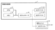
図15及び図16は、I2Cバスを有する情報処理装置100及び100′の構成例を示す図である。
はじめに、図15に示す例を説明する。図15に示すように、情報処理装置100は、MPU(Micro Processing Unit)120、I2Cバスコントローラ130、IO_PORT入力110、IO_PORT出力111、並びに、バススイッチ140a及び140bを備える。また、情報処理装置100は、プルアップ抵抗150及び160、コネクタ170、電源供給部180、並びに、I2Cデバイス210−2及び210−3を備える。さらに、追加ユニット200は、I2Cデバイス210−1、電源部220、及び、コネクタ230を備える。In order to prevent malfunction of other devices due to addition of a unit to the 2-wire serial bus, for example, the following method is known.
15 and 16 are diagrams illustrating configuration examples of the
First, an example shown in FIG. 15 will be described. As illustrated in FIG. 15, the
MPU120は、I2Cデバイス210−1〜210−3(以下、I2Cデバイス210−1〜210−3を区別しない場合には、単にI2Cデバイス210という)の監視及び制御を行なうプロセッサである。MPU120は、ローカルバス310を介してIO_PORT入力110、IO_PORT出力111、及び、I2Cバスコントローラ130に接続される。
The MPU 120 is a processor that monitors and controls the I2C devices 210-1 to 210-3 (hereinafter, simply referred to as the
IO_PORT入力110は、情報処理装置100に追加ユニット200が実装されたことを検出する。ここで、IO_PORT入力110は、プルアップ抵抗160により所定の電圧レベルに維持された実装信号線340を介して、コネクタ170に接続される。また、追加ユニット200のコネクタ230には、GND接続(接地)された実装信号線420が接続される。コネクタ170がコネクタ230に接続されると、実装信号線340が実装信号線420を介してGND接続する。このため、IO_PORT入力110は、実装信号線340の電圧が低下した場合に、情報処理装置100に追加ユニット200が実装されたことを検出する。
The IO_PORT
I2Cバスコントローラ130は、プルアップ抵抗150により所定の電圧レベルに維持されたシリアルバス(I2Cバス)320を介してI2Cデバイス210と接続され、I2Cデバイス210との間でデータ信号及びクロック信号の通信制御を行なう。
BUS−SW(バススイッチ)140a及び140bは、それぞれ、シリアルバス320に含まれるデータ信号線(SDA)320a及びクロック信号線(SCL)320bとコネクタ170との間に介装されるスイッチである。バススイッチ140a及び140bは、対応する信号線とコネクタ170及び230を介して接続された追加ユニット200のI2Cデバイス210−1との間の接続を切り替える。なお、バススイッチ140a及び140bは、コネクタ170に追加ユニット200が接続されるときにはいずれもディセーブル状態になり、シリアルバス320とI2Cデバイス210−1との間の接続を開放、つまり切り離された状態にする。The
The BUS-SWs (bus switches) 140a and 140b are switches interposed between the data signal line (SDA) 320a and the clock signal line (SCL) 320b included in the serial bus 320 and the connector 170, respectively. The
IO_PORT出力111は、MPU120からの制御に応じて、制御線330a及び330bを介してバススイッチ140a及び140bにおける接続の切り替えを行なう。
なお、電源供給部180は、コネクタ170に追加ユニット200のコネクタ230が接続されると、電源部220に対して電力を供給する。
上述の如く構成された情報処理装置100では、追加ユニット200が実装されると、IO_PORT110は、実装信号線340の実装信号がHighからLowに変化したことを通じて追加ユニット200の接続を検知する(図15の矢印(1)参照)。The IO_PORT
The
In the
MPU120は、IO_PORT入力110を参照して追加ユニット200が接続されたことを認識すると、I2Cバスコントローラ130に対して、シリアルバス320のバスアクセスの動作を一旦停止させる(図15の矢印(2)参照)。
また、MPU120は、シリアルバス320が停止している間に、IO_PORT出力111を制御してバススイッチ140a及び140bをイネーブルに切り替える(図15の矢印(3)参照)。これにより、バススイッチ140a及び140bが閉じて、SDA320aと追加ユニット200のSDA410aとが導通するとともに、SCL320bと追加ユニット200のSCL410bとが導通する。When the MPU 120 recognizes that the
Also, the MPU 120 controls the
バススイッチ140a及び140bがイネーブルに切り替えられると、I2Cバスコントローラ130は、バスアクセスの動作を再開し、追加ユニット200のI2Cデバイス210−1へのバスアクセスを実施する(図15の矢印(4)参照)。
以上の動作により、MPU120は、シリアルバス320のバスアクセスを一旦停止させて、シリアルバス320へ追加ユニット200を接続させる。これにより、追加ユニット200の信号線のコンデンサ成分(浮遊容量)による、バス線への追加ユニット200の接触時のノイズ(電圧低下)の影響を抑えることができる。つまり、追加ユニット200をコネクタ170に接続した際に発生する電圧低下のノイズは、ディセーブル状態のバススイッチ140a及び140bにより分離されるため、シリアルバス320には影響を及ぼさない。When the
With the above operation, the MPU 120 temporarily stops the bus access of the serial bus 320 and connects the
次に、図16に示す例を説明する。図16に示すように、情報処理装置100′は、図15に示す情報処理装置100と同様の構成を備えるが、IO_PORT出力111、並びに、バススイッチ140a及び140bの代わりに、I2Cバスマルチプレクサ112を備える点が異なる。
I2Cバスマルチプレクサ112は、シリアルバス320とI2Cデバイス210及びコネクタ170との間に介装されるI2Cデバイスである。なお、I2Cバスマルチプレクサ112としては、NXP製PCA9542等が挙げられる。Next, an example shown in FIG. 16 will be described. As shown in FIG. 16, the
The
I2Cバスマルチプレクサ112は、情報処理装置100′内部のI2Cデバイス210−2及び210−3用のチャネル1と、追加ユニット200のI2Cデバイス210−1用のチャネル2との間で、シリアルバス320のチャネル切替を行なう。具体的には、I2Cバスマルチプレクサ112は、バスがビジー状態でないタイミングでチャネル切替を行なう。なお、I2Cバスマルチプレクサ112は、内部にレジスタを備え、I2Cコントローラ130を介してMPU120によりチャネル切替を示す値がレジスタに書き込まれると、バスがビジー状態でないタイミングの検出を開始する。
The
上述の如く構成された情報処理装置100′では、追加ユニット200が実装されると、IO_PORT110は、情報処理装置100と同様に追加ユニット200の接続を検知する(図16の矢印(1)参照)。
MPU120は、追加ユニット200の接続の検出後、追加ユニット200へのアクセスに先立ち、シリアルバス320を介して、I2Cバスマルチプレクサ112の内部レジスタに対してチャネル切替制御を行なう(図16の矢印(2′)参照)。
In the
MPU120 after detection of the connection of the
I2Cバスマルチプレクサ112は、内部レジスタの値に基づき、バスがビジー状態でないタイミングでチャネル1からチャネル2への切り替えを行なう(図16の矢印(3′)参照)。
I2Cバスマルチプレクサ112によりチャネルが切り替えられると、I2Cバスコントローラ130は、追加ユニット200のI2Cデバイス210−1へのバスアクセスを実施する(図16の矢印(4)参照)。Based on the value of the internal register, the
When the channel is switched by the
以上の動作により、I2Cバスマルチプレクサ112は、バスがビジー状態でないときに、チャネルを切り替えてシリアルバス320へ追加ユニット200を接続させる。これにより、図15に示す例と同様に、追加ユニット200の信号線のコンデンサ成分(浮遊容量)による、バス線への追加ユニット200の接触時のノイズ(電圧低下)の影響を抑えることができる。つまり、追加ユニット200をコネクタ170に接続した際に発生する電圧低下のノイズは、I2Cバスマルチプレクサ112により分離されるため、シリアルバス320には影響を及ぼさない。
With the above operation, the
なお、関連する技術として、システムのオンライン稼働中でのモジュールの交換手法が知られている(例えば、特許文献1参照)。この技術では、モジュールの挿入/抜去のときに発生するノイズをバスに接続された他のモジュールが受信しても誤動作しないタイミングで、バススイッチがモジュールの接続/切り離しを行なう。
ここで、ノイズを他のモジュールが受信しても誤動作しないタイミングとしては、図17に示す例が挙げられる。図17は、バスへのモジュールの接続又は切り離しのタイミングを説明する図である。例えばパラレルバスでは、他のモジュールは、バスクロックの立ち上がりのタイミングでデータを受け取る。換言すれば、他のモジュールは、追加モジュールをバスへ接続した際にノイズが発生したとしても、バスクロックに同期してデータを受け取るときにこのノイズが消滅していれば、ノイズの影響を受けずにデータ(図17のデータ“B”)を受け取ることができる。As a related technique, a module replacement method during online operation of the system is known (for example, see Patent Document 1). In this technique, the bus switch connects / disconnects modules at a timing that does not cause a malfunction even when other modules connected to the bus receive noise generated when the modules are inserted / removed.
Here, an example shown in FIG. 17 is given as a timing at which no malfunction occurs even when other modules receive noise. FIG. 17 is a diagram for explaining the timing of connecting or disconnecting the module to the bus. For example, in the parallel bus, other modules receive data at the rising timing of the bus clock. In other words, even if noise occurs when another module is connected to the bus, other modules are affected by the noise if the noise disappears when data is received in synchronization with the bus clock. The data (data “B” in FIG. 17) can be received.
また、関連する他の技術として、バスとユニットとの間に介装されたスイッチにより、バス又はユニットの状態に応じて、バス及びユニットの接続状態を切り替える技術が知られている(例えば、特許文献2及び3参照)。
さらに、コンピュータ本体のバスの電位レベルを制御し、拡張ユニット側のバスと等しい電位レベルにすることで、バスサイクルが実行状態のときに、拡張ユニットとのバス接続を可能とする技術が知られている(例えば、特許文献4参照)。As another related technique, a technique is known in which the connection state of the bus and the unit is switched according to the state of the bus or the unit by a switch interposed between the bus and the unit (for example, a patent).
Furthermore, a technology is known that enables the bus connection with the expansion unit when the bus cycle is in an execution state by controlling the potential level of the bus of the computer main body and setting it to the same potential level as the bus on the expansion unit side. (For example, see Patent Document 4).
図15に示す情報処理装置100では、MPU120は、I2Cバスコントローラ130に対するソフトウェアによる制御により、I2Cバス320の動作を停止させる。本来、I2Cバス320のような共有バスは、常にデバイスへアクセスできる状態であることが望ましいが、情報処理装置100においては、共有バスへの追加ユニット200の接続の際に、他のデバイス210に対して継続アクセスができなくなる。
In the
また、図16に示す情報処理装置100′では、I2Cバスマルチプレクサ112が備えられることでI2Cバス320が分岐しバス構成が複雑になる。MPU120は、複雑なバス構成へ追加ユニット200を追加するために、I2Cバスマルチプレクサ112に対してソフトウェアによるチャネル切替制御を行なう。従って、情報処理装置100′では、図15に示す情報処理装置100と同様の問題に加え、MPU120によるチャネル切替制御において処理の遅延が発生するという問題もある。
In addition, in the
さらに、図17を参照して説明した技術は、パラレルバスに適用されるものである。仮に、当該技術をI2C(シリアル)バスに適用したとしても、追加するモジュールの接続に伴いクロック信号にノイズが発生した場合には、他のモジュールは誤ってデータを取りこんでしまう可能性がある。
なお、上述した、バス又はユニットの状態に応じてスイッチによりバス及びユニットの接続状態を切り替える技術では、ユニットを接続する際に発生するノイズの影響を抑えることについては考慮されていない。Furthermore, the technique described with reference to FIG. 17 is applied to a parallel bus. Even if the technology is applied to an I2C (serial) bus, if noise occurs in the clock signal due to the connection of the added module, other modules may erroneously capture data.
Note that the above-described technology for switching the connection state between the bus and the unit with a switch according to the state of the bus or the unit does not consider the suppression of the influence of noise generated when the units are connected.
また、コンピュータ本体のバスの電位レベルを制御し、拡張ユニット側のバスと等しい電位レベルにする技術では、ソフトウェアによる複雑な制御が行なわれるため、拡張ユニットの接続処理の遅延が発生するという問題がある。
以上のように、上述した技術では、デバイスの接続の際にバスは種々の影響を受ける。
1つの側面では、本発明は、デバイスの接続の際にバスが受ける影響を低減させることを目的とする。In addition, in the technology for controlling the potential level of the bus of the computer main body to be equal to the potential level of the bus on the expansion unit side, complicated control by software is performed, so that there is a problem in that the expansion unit connection processing is delayed. is there.
As described above, in the above-described technique, the bus is affected in various ways when devices are connected.
In one aspect, the present invention is directed to reducing the impact of the bus upon device connection.
なお、前記目的に限らず、後述する発明を実施するための形態に示す各構成により導かれる作用効果であって、従来の技術によっては得られない作用効果を奏することも本発明の他の目的の1つとして位置付けることができる。 In addition, the present invention is not limited to the above-described object, and other effects of the present invention can be achieved by the functions and effects derived from the respective configurations shown in the embodiments for carrying out the invention which will be described later. It can be positioned as one of
本件の接続制御装置は、バスに対するデバイスの接続制御を行なう接続制御装置であって、前記バスに含まれる複数の信号線の各々から入力される信号の電圧レベルの組み合わせに基づき前記バスのバスサイクルの開始タイミングを検出した場合、前記複数の信号線の各々から入力される信号の電圧レベルがそれぞれ所定の閾値未満であることを検出する検出部と、前記バスと前記デバイスとの間に介装され前記複数の信号線の各々と前記デバイスとの間の接続の切り替えを行なう切替部に対して、前記検出部により前記信号の電圧レベルが前記所定の閾値未満であることが検出された信号線を前記デバイスに接続させるように切替制御を行なう切替制御部と、をそなえる。 The connection control device according to the present invention is a connection control device that controls connection of a device to a bus, and is based on a combination of voltage levels of signals input from a plurality of signal lines included in the bus. when detecting the start timing, interposed between a detector for detecting the voltage level of a signal input from each of said plurality of signal lines are each less than a predetermined threshold value, and the bus and said device against switching unit for switching the connection between is between said device and each of said plurality of signal lines are signal line voltage level of the signal by the detecting unit is detected that the less than a predetermined threshold value And a switching control unit that performs switching control so as to be connected to the device.
第1又は第2実施形態によれば、デバイスの接続の際にバスが受ける影響を低減させることができる。 According to the first or second embodiment, it is possible to reduce the influence of the bus upon connection of devices.
以下、図面を参照して実施の形態を説明する。
〔1〕第1実施形態
〔1−1〕情報処理装置の説明
図1は、第1実施形態に係る情報処理装置1の構成例を示す図である。図1に示すように、情報処理装置1は、I2Cコントローラ50、Central Processing Unit(CPU)51、メモリ52、並びに、I2Cデバイス21−2及び21−3を備える。Hereinafter, embodiments will be described with reference to the drawings.
[1] First Embodiment [1-1] Description of Information Processing Device FIG. 1 is a diagram illustrating a configuration example of an
CPU(プロセッサ)51は、種々の制御や演算を行なう処理装置である。CPU51は、メモリ52又は図示しないRead Only Memory(ROM)等に格納されたプログラムを実行することにより、種々の機能を実現する。なお、CPU51は、メモリ52及びI2Cコントローラ50とそれぞれシステムバスを介して接続される。
メモリ52は、種々のデータやプログラムを一時的に格納する記憶装置であって、CPU51がプログラムを実行する際に、データやプログラムを一時的に格納・展開して用いる。なお、メモリ52としては、例えばRandom Access Memory(RAM)等の揮発性メモリが挙げられる。The CPU (processor) 51 is a processing device that performs various controls and operations. The
The
I2Cコントローラ50は、2線式のシリアルバスの一例であるI2Cバスを介して、I2Cデバイス21−2及び21−3に対する各種制御を行なう装置である。また、第1実施形態に係るI2Cコントローラ50は、I2Cデバイス21−1を備える追加ユニット(I2Cユニット)20をI2Cバスに接続させるために、後述する各種制御を行なう。例えば、I2Cコントローラ50は、I2Cデバイス21を含む情報処理装置1の監視を行なう監視装置であってもよい。
The
I2Cデバイス21−1〜21−3(I2Cデバイス21−1〜21−3を区別しない場合には、単にI2Cデバイス21という)は、情報処理装置1に対して活線接続が可能なデバイスである。例えば、I2Cデバイス21としては、Hard Disk Drive(HDD)又はSolid State Drive(SSD)等の記憶装置のほか、ファン、センサ、電源等の制御装置、又は、監視装置等、I2Cに準拠した種々のデバイスが挙げられる。
The I2C devices 21-1 to 21-3 (in the case where the I2C devices 21-1 to 21-3 are not distinguished from each other) are simply devices that can be hot-wired to the
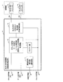
〔1−2〕I2Cコントローラの説明
次に、図2を参照してI2Cコントローラ50の構成を説明する。
図2は、図1に示すI2Cコントローラ50の構成例を示す図である。
図2に示すように、I2Cコントローラ50は、BUS−SW(バススイッチ)制御部10、MPU2、I2Cバスコントローラ3、バススイッチ4a及び4b、プルアップ抵抗5及び6、コネクタ7、電源供給部8、並びに、クロック発振器9を備える。[1-2] Description of I2C Controller Next, the configuration of the
FIG. 2 is a diagram illustrating a configuration example of the
As shown in FIG. 2, the
また、追加ユニット20は、図15又は図16に示す追加ユニット200と同様の構成であり、I2Cデバイス21−1、電源部22、及び、コネクタ23を備える。
MPU2は、図示しないROM等に格納されたファームウェアを実行することにより種々の制御を実行するプロセッサである。例えば、MPU2は、ローカルバス31を介してI2Cバスコントローラ3に接続され、I2Cデバイス21−1〜21−3の監視及び制御を行なう。The
The
I2Cバスコントローラ3は、プルアップ抵抗5により所定の電圧レベルに維持されたシリアルバス(バス)32を介してI2Cデバイス21と接続され、MPU2からの制御を受けてI2Cデバイス21との間でデータ信号及びクロック信号の通信制御を行なう。
つまり、図2に示すように、シリアルバス32に含まれるデータ信号線(SDA)32a及びクロック信号線(SCL)32bは、それぞれプルアップ抵抗5に接続され、プルアップ抵抗5により各信号線の電圧が調整される。例えば、SDA32a及びSCL32bの各々は、I2Cバスコントローラ3により印加された電圧レベルがVhigh(High)又はVlow(Low)で示す所定のレベルを維持するように、プルアップ抵抗5によって調整される(図4及び図5参照)。The
That is, as shown in FIG. 2, the data signal line (SDA) 32 a and the clock signal line (SCL) 32 b included in the
なお、図2において図示を省略しているが、MPU2及びI2Cバスコントローラ3の少なくとも一方は、システムバスを介して図1に示すCPU51に接続され、CPU51からの要求に応じて、上記制御を行なうのである。
BUS−SW(バススイッチ,スイッチ)4a及び4bは、それぞれ、SDA32a及びSCL32bとコネクタ7との間に介装されるスイッチである。バススイッチ14a及び14bは、対応する信号線について個別に、コネクタ7及び23を介して接続された追加ユニット20(I2Cデバイス21−1)との間の接続及び切り離しの切り替えを行なう。なお、バススイッチ4a及び4bは、コネクタ7に追加ユニット20が接続されるときにはいずれもディセーブル状態になり、シリアルバス32とI2Cデバイス21−1との間の接続を開放、つまり切り離された状態にする。Although not shown in FIG. 2, at least one of the
The BUS-SWs (bus switches, switches) 4a and 4b are switches interposed between the
従って、バススイッチ4a及び4bは、シリアルバス32とI2Cデバイス21−1との間に介装され複数の信号線(SDA32a及びSCL32b)の各々とI2Cデバイス21との間の接続の切り替えを行なう切替部4の一例である。なお、ここでは、切替部4がバススイッチ4a及び4bである例を説明したが、これに限定されるものではなく、複数の信号線とI2Cデバイス21との間の接続の切り替えを個別に行なうことができれば、切替部4が一のスイッチ素子により実現されてもよい。
Accordingly, the
コネクタ7は、追加ユニット20のコネクタ23と嵌合等によって接触することにより、I2Cコントローラ50と追加ユニット20とを接続する。具体的には、コネクタ7は、I2Cコントローラ50側のSDA32a、SCL32b、実装信号線34、電源供給部8と、追加ユニット20側のSDA41a、SCL41b、実装信号線42、電源部22と、をそれぞれ接触(導通)させる。
The
実装信号線34は、バススイッチ制御部10とコネクタ7とを接続する信号線であり、プルアップ抵抗6により所定の電圧レベルに維持される。一方、追加ユニット20のコネクタ23には、GND接続(接地)された実装信号線42が接続されている。
電源供給部8は、コネクタ7に追加ユニット20のコネクタ23が接続されると、電源部22に対して電力を供給する。The mounting
The
クロック発振器9は、バススイッチ制御部10においてサンプリングを行なうために用いられるクロック信号を生成するものである。なお、クロック発振器9が生成するクロック信号は、SDA32aにおけるクロック信号よりも十分に早い(例えば十倍程度の)周波数である。なお、クロック発振器9としては、LC回路を用いた発振器や水晶発振器等が挙げられる。
The
バススイッチ制御部(接続制御装置)10は、シリアルバス32に対するI2Cデバイス21の接続制御を行なう装置である。バススイッチ制御部10は、図2に示すように、シリアルバス32から分岐したSDA32a及びSCL32b、実装信号線34、並びに、クロック発振器9からのクロック信号線35が接続され、各信号線からの信号を入力信号とする。また、バススイッチ制御部10は、図2に示すように、バススイッチ4a及び4bの各々とBUS−SW ENABLE(バススイッチイネーブル;以下、制御線という)33a及び33bを介して接続され、バススイッチ4a及び4bを制御する。
The bus switch control unit (connection control device) 10 is a device that controls connection of the
以下、図3〜図6を参照してバススイッチ制御部10の構成を説明する。図3は、図2に示すバススイッチ制御部10の構成例を示す図であり、図4及び図5は、それぞれ、図2に示すシリアルバス32へ追加ユニット20を活線挿入したときのシリアルバス32の電圧レベルを説明する図である。図6は、図2に示すシリアルバス32の通信状態の遷移を説明する図である。
Hereinafter, the configuration of the bus
図3に示すように、バススイッチ制御部10は、実装信号検知部11、タイマー部12、クロック信号/データ信号レベル判定部13、BUS−SW ENABLE(バススイッチイネーブル)設定部14を備える。
実装信号検知部(検知部)11は、実装信号線34からの実装信号を入力され、I2Cユニット20(I2Cデバイス21)がコネクタ7(バススイッチ4a及び4b)に接続されたことを検知する。例えば、コネクタ7がコネクタ23に接続されると、実装信号線34は、実装信号線42を介してGND接続する。実装信号検知部11は、実装信号線42の電圧が低下したことを検知すると、I2Cデバイス21がバススイッチ4a及び4bに接続されたことを検知する。As shown in FIG. 3, the bus
The mounting signal detection unit (detection unit) 11 receives a mounting signal from the mounting
タイマー部12は、所定期間の計時を行なうものである。タイマー部12としては、例えばカウンター回路のほか、計時が可能な種々の回路を用いることができる。
バススイッチイネーブル設定部(切替制御部)14は、切替部4に対して、後述する信号レベル判定部13により信号の強度(電圧レベル)が所定の閾値未満であると判定された信号線をI2Cデバイス21に接続させるように切替制御を行なう。具体的には、バススイッチイネーブル設定部14は、信号レベル判定部13により検出されたSDA32a又はSCL32bに対応するバススイッチ4a又は4bに対して、切り離し状態から接続状態に切り替えさせる制御を行なう。The
The bus switch enable setting unit (switching control unit) 14 sends to the
例えば、バススイッチイネーブル設定部14は、追加ユニット20がI2Cコントローラ50に接続されたときは、制御線33a及び33bの電圧レベルをLow(ディセーブル)にすることで、バススイッチ4a及び4bを開放し、切り離し状態にする。一方、バススイッチイネーブル設定部14は、信号レベル判定部13からの指示に応じて、制御線33a又は33bの電圧レベルをHigh(イネーブル)にすることで、バススイッチ4a又は4bを閉じ、接続状態にする。
For example, when the
クロック信号/データ信号レベル判定部(信号レベル判定部,判定部)13は、追加ユニット20をシリアルバス32へ接触させる際に発生する、追加ユニット20内の信号線のコンデンサ成分によるノイズの大きさが最小限となるタイミングを検出する。
具体的には、信号レベル判定部13は、実装信号検知部11によりI2Cデバイス21がバススイッチ4a及び4bに接続されたことが検知されると、SDA32a及びSCL32bの各々から入力される信号の電圧レベルを監視する。そして、信号レベル判定部13は、SDA32a及びSCL32bの各々から入力される信号の電圧レベルが所定の閾値(Vthreshold)未満であるか否かを判定する。より具体的に、信号レベル判定部13は、クロック発振器9から入力されるクロック信号を用いて、SDA32a及びSCL32bから入力される信号をそれぞれサンプリングする。そして、信号レベル判定部13は、サンプリング結果から、各信号の電圧レベルがHigh及びLowのいずれの状態であるかを判別する。The clock signal / data signal level determination unit (signal level determination unit, determination unit) 13 generates noise when the
Specifically, when the mounting
以下、図4及び図5を参照して、シリアルバス32へ追加ユニット20を活線挿入するタイミングと、シリアルバス32の電圧レベルとの関係を説明する。
図4に示すように、シリアルバス32のうちのSDA32a又はSCL32bの信号の電圧レベルがVhighである場合、図4中“接触”のタイミングでシリアルバス32に追加ユニット20が接続されると、浮遊容量による電圧低下の振れが大きい。図4に示す例では、SDA32a又はSCL32bの電圧レベルは、閾値(Vthreshold)の近傍にまで降下しているため、システムバス32に接続された他のI2Cデバイス21が誤動作する可能性がある。Hereinafter, with reference to FIG. 4 and FIG. 5, the relationship between the timing when the
As shown in FIG. 4, when the voltage level of the signal of the
これに対し、図5に示すように、SDA32a又はSCL32bの信号の電圧レベルがVlowである場合、もともと電圧レベルがLowの状態であるため、浮遊容量に起因する電圧低下が発生しても他のI2Cデバイス21で誤動作は生じない。つまり、バス線の電圧レベルがLowの状態のときに、システムバス32に追加ユニット20を接続することで、追加ユニット20のコンデンサ成分によるノイズの影響を抑えることができる。
On the other hand, as shown in FIG. 5, when the voltage level of the
そこで、信号レベル判定部13は、上述のようにバス線の電圧レベルがLowになったタイミングを判定し、Lowになったバス線(SDA32a又はSCL32b)について、バススイッチイネーブル設定部14に切替制御を指示する。
ここで、シリアルバス32の一例としてのI2Cバスは、図6に示すように、通信の過程で、バスアクセスとバスアクセスとの合間であるバスフリータイム(Bus free time between STOP and START conditions;以下、Tbufという)の状態に遷移する。Tbufは、STOPコンディションとSTARTコンディションとの間の時間であり、この間、シリアルバス32に接続されたI2Cデバイス21−2及び21−3は、シリアルバス32を使用しない。Therefore, the signal
Here, as shown in FIG. 6, the I2C bus as an example of the
I2CバスのSTARTコンディションは、図6に示すように、SCL32bがHighの状態のときに、SDA32aがHighの状態からLowに落ちるときの状態であり、I2Cバスにおけるバスアクセスの開始を表す。一方、I2CバスのSTOPコンディションは、図6に示すように、SCL32bがHighの状態のときに、SDA32aがLowの状態からHighに上がるときの状態であり、I2Cバスにおけるバスアクセスの終了を表す。
As shown in FIG. 6, the START condition of the I2C bus is a state when the
図6に示すように、SDA32a及びSCL32bは、STARTコンディションにおいて、順にHighの状態からLowに落ちる。
そこで、信号レベル判定部13は、Tbufを検出し、その後のSTARTコンディションを検出することで、SDA32a及びSCL32bの電圧レベルについて、HighからLowへの切り替わりを、順に検出することができる。そして、信号レベル判定部13は、Lowへの切り替わりを検出したSDA32a及びSCL32bについて、個別にバススイッチ4a及び4b(バススイッチイネーブル設定部14)に対して切替制御を行なうことができる。As shown in FIG. 6, the
Therefore, the signal
すなわち、信号レベル判定部13は、SDA32a及びSCL32bの各々から入力される信号の電圧レベルが、タイマー部12による所定期間の計時の間、いずれも所定の閾値(Vthreshold)以上である場合に、Tbufの期間であると判定する。ここで、Tbufは、I2Cバス固有の期間であり、SCL32bのクロック信号におけるHighの期間よりも長い。従って、タイマー部12には、計時する期間として、予めTbufと同一或いは略同一、又はTbuf以上の期間が設定されることが好ましい。
That is, the signal
〔1−3〕バススイッチ制御部の詳細な構成例
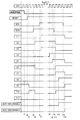
次に、図7及び図8を参照して、バススイッチ制御部10の詳細な構成例を説明する。図7は、図2に示すバススイッチ制御部10の詳細な構成例を示す図であり、図8は、図7に示すバススイッチ制御部10における各部の状態の一例を示すタイムチャートである。図7に示すように、バススイッチ制御部10は、例えば複数の回路素子を用いて、ハードウェアにより実現される。[1-3] Detailed Configuration Example of Bus Switch Control Unit Next, a detailed configuration example of the bus
実装信号検知部11は、実装信号線34に接続される抵抗11a、増幅器11b、及びコンデンサ11cを備える。
タイマー部12は、カウンター回路12a及びOR回路10cを備える。
信号レベル判定部13は、プルアップ抵抗10a、10e、及び10k、AND回路10b、10f、及び10l、OR回路10i、NAND回路10j、並びにDelay−Flip Flop(ディレイフリップフロップ;D−FF)13a〜13fを備える。The mounting
The
The signal
バススイッチイネーブル設定部14は、プルアップ抵抗10h及び10n、OR回路10g及び10m、並びにD−FF14a及び14bを備える。
なお、図7において、“RESET”は、例えばMPU2から送信されるリセット信号線36であり、実装信号線34がLowに落ちると、Highに維持される。
以下、クロック発振器9からのクロック信号線35、実装信号検知部11からの実装信号線34、リセット信号線36、SCL32b、SDA32a、図7に示す(1)〜(11)の各部、並びに制御線33a及び33bの状態の一例を、図8を参照して説明する。なお、図8においては、制御線33aを“BUS−SW1_ENABLE”と表記し、制御線33bを“BUS−SW2_ENABLE”と表記する。The bus switch enable setting
In FIG. 7, “RESET” is, for example, the
Hereinafter, the
なお、クロック発振器9からのクロック信号線35は、サンプリング用のクロック信号を出力し、バススイッチ制御部10内の各回路素子は、クロック信号に同期して動作を行なう。
タイミングt1において、実装信号線34がLow、つまり追加ユニット20がシステムバス32に接続されると、リセット信号線36がHighに維持される(タイミングt2)。また、タイミングt3において、D−FF13eの出力(9)がHighからLowに遷移するとともに、D−FF13fの出力(10)がLowからHighに遷移する。The
When the mounting
タイミングt4において、SDA32aの電圧レベルがLowからHighに遷移すると、D−FF13aの出力(2)がHighになるとともに、D−FF13c及び13eの出力(6)及び(10)がそれぞれLowになる(タイミングt5)。なお、D−FF13a、13c、及び13eは、それぞれSDA32aの電圧レベルを監視するD−FFである。
When the voltage level of the
次いで、タイミングt6において、SCL32bの電圧レベルがLowからHighに遷移すると、D−FF13bの出力(1)がHighになる(タイミングt7)。また、タイミングt7において、D−FF13a及び13bの出力のANDをとるAND回路10bの出力(3)がHighになる(タイミングt7)。なお、D−FF13b、13d、及び13fは、それぞれSCL32bの電圧レベルを監視するD−FFである。
Next, when the voltage level of the
なお、タイミングt6において、SDA32aの電圧レベルがHighの状態で、SCL32bの電圧レベルがHighに遷移したため(STOPコンディション)、システムバス32はバスフリータイムの状態になっている。
カウンター回路12aでは、AND回路10bの出力(3)がHighになったことで、“*LOAD”端子にHighが入力される。そして、カウンター回路12aは、タイミングt7において、Tbufの期間のカウントを開始する。At timing t6, since the voltage level of
In the
カウンター回路12aによる所定期間の計時が終了し、AND回路10bの出力(3)がHighである時間がTbuf以上であった場合には、カウンター回路12aの出力(4)がHighに遷移する(タイミングt8)。また、出力(4)がHighになったことにより、カウンター回路12aの後段のD−FF13dの出力(5)がHighに遷移する(タイミングt9)。
When the counting of the predetermined period by the
ここで、タイミングt10において、SDA32aの電圧レベルがHighからLowに遷移すると、つまりSTARTコンディションになると、D−FF13a及びAND回路10bの出力(2)及び(3)がLowになる(タイミングt11)。また、タイミングt11において、D−FF13c及び13eの出力(6)及び(10)がHighになるとともに、D−FF13c及び13dのANDをとるAND回路10fの出力(7)がHighになる。
Here, at the timing t10, when the voltage level of the
また、AND回路10fの出力(7)がHighになったことで、D−FF14aの出力(8)がHighになり、制御線33aの電圧レベルがHighになる(タイミングt12)。すなわち、バススイッチイネーブル設定部14によりバススイッチ4aが接続状態に切替制御され、I2Cデバイス21−1のSDA42aがシリアルバス32のSDA32aに接続される。
Also, since the output (7) of the AND
次いで、タイミングt13において、SCL32bの電圧レベルがHighからLowに遷移すると、D−FF13b及び13dの出力(1)及び(5)がLowに遷移する(タイミングt14)。また、タイミングt14において、D−FF13c及び13dのANDをとるAND回路10fの出力(7)がLowになる。さらに、タイミングt14において、D−FF13fの出力(9)がHighに遷移するとともに、D−FF13e及び13fのANDをとるAND回路10lの出力(11)がHighになる。
Next, when the voltage level of the
また、AND回路10lの出力(11)がHighになったことで、D−FF14bの出力がHighになり、制御線33bの電圧レベルがHighになる(タイミングt14)。すなわち、バススイッチイネーブル設定部14によりバススイッチ4bが接続状態に切替制御され、I2Cデバイス21−1のSCL41bがシリアルバス32のSCL32bに接続される。
In addition, since the output (11) of the AND circuit 101 becomes High, the output of the D-
以上のように、第1実施形態に係るバススイッチ制御部10によれば、信号レベル判定部13及びバススイッチイネーブル設定部14が論理回路により実現される。従って、I2Cバスの動作の中で、追加ユニット20をシリアルバス32に接続する機会をハードウェアによって高速に検出し接続を行なうため、図15を参照して説明したソフトウェアによる制御と比べ、I2Cバスコントローラ3の動作を停止しなくてよい。さらに、図16を参照して説明したI2Cバスマルチプレクサ112のように、バス分岐がなくなるため、バス構成が複雑になることを抑止できる。また、ハードウェアによる制御は、MPU2の性能や負荷に依存するソフトウェアによる制御と比べて、安定した動作を実現することができる。
As described above, according to the bus
なお、図17を参照して説明したパラレルバスに関する技術をI2Cバスに適用した場合、I2Cバスにはバス制御信号がないため、I2Cデバイス21は、発生したノイズが原因でSTARTコンディション又はSTOPコンディションと誤認識する可能性がある。これに対し、第1実施形態に係るバススイッチ制御部10によれば、バス線の電圧レベルがLowの状態のときに、システムバス32に追加ユニット20を接続するため、I2Cデバイス21は、発生するノイズが原因でシリアルバス32の状態を誤認識することがない。
When the technology related to the parallel bus described with reference to FIG. 17 is applied to the I2C bus, the
なお、図7では、信号レベル判定部13及びバススイッチイネーブル設定部14の双方が論理回路により実現される例を示したが、これに限定されるものではない。例えば、信号レベル判定部13及びバススイッチイネーブル設定部14のうちの少なくとも一方が論理回路をそなえる構成としてもよい。この場合でも、信号レベル判定部13及びバススイッチイネーブル設定部14の双方がソフトウェアによる制御により実現される場合と比べて、安定した動作を実現することができる。
Although FIG. 7 shows an example in which both the signal
〔1−4〕第1実施形態の動作例
次に、上述の如く構成された第1実施形態に係るI2Cコントローラ50における、シリアルバス32への追加ユニット20(I2Cデバイス21−1)の接続制御の動作例を、図9〜図11を参照して説明する。図9は、図1に示すI2Cコントローラ50の動作例を説明するフローチャートであり、図10は、図1に示すI2Cコントローラ50の動作例を説明する図である。図11は、図2に示すシリアルバス32、実装信号線34、及び制御線33の状態の一例を示すタイムチャートである。なお、図9においては、制御線33aを“BUS−SW1_ENABLE”と表記し、制御線33bを“BUS−SW2_ENABLE”と表記する。[1-4] Operation Example of First Embodiment Next, connection control of the additional unit 20 (I2C device 21-1) to the
はじめに、図9に示すように、バススイッチ制御部10により、追加ユニット20がコネクタ7に接続されたことに起因する実装信号が検出されたか否かが判定される(ステップS1)。実装信号が検出されなかったと判定された場合(ステップS1のNoルート)、実装信号が検出されるまでステップS1の判定が行なわれる。
一方、実装信号が検出されたと判定された場合(ステップS1のYesルート;図10の矢印(1)及び図11のタイミングT1参照)、バススイッチ制御部10により、バスフリータイム(Tbuf)が検出されたか否かが判定される(ステップS2)。つまり、バススイッチ制御部10は、シリアルバス32のSDA32a及びSCL32bの電圧レベルを監視し、両方とも一定時間(Tbuf)High状態であるバスフリータイム(バスアクセスとバスアクセスとの合間)の検出が行なわれる。バススイッチ制御部10により、Tbufが検出されなかったと判定された場合(ステップS2のNoルート)、Tbufが検出されるまでステップS2の判定が行なわれる。First, as shown in FIG. 9, the bus
On the other hand, if it is determined that a mounting signal has been detected (Yes route in step S1; see the arrow (1) in FIG. 10 and the timing T1 in FIG. 11), the bus
一方、Tbufが検出されたと判定された場合(ステップS2のYesルート;図10の(2)及び図11のタイミングT1〜T2参照)、バススイッチ制御部10により、SDA32aの電圧レベルがHighからLowに遷移したことが検出されたか否かが判定される(ステップS3)。つまり、バススイッチ制御部10は、バスフリータイムを検出すると、I2CバスのSTARTコンディションの発生を検出する。バススイッチ制御部10により、SDA32aの電圧レベルがHighからLowに遷移したことが検出されなかったと判定された場合(ステップS3のNoルート)、遷移したことが検出されるまでステップS3の判定が行なわれる。
On the other hand, when it is determined that Tbuf has been detected (Yes route in step S2; see timings T1 to T2 in FIG. 10 (2) and FIG. 11), the voltage level of the
これに対し、ステップS3において、SDA32aの電圧レベルがHighからLowに遷移したことが検出されたと判定された場合(ステップS3のYesルート;図10の矢印(3)及び図11のタイミングT2参照)、ステップS4に移行する。
ステップS4では、バススイッチ制御部10により、制御線33aがイネーブルにされ、バススイッチ4aが閉じられることで、SDA32aとSDA41aとが接続される(図10の矢印(4)及び(5)並びに図11のタイミングT3参照)。つまり、バススイッチ制御部10は、SDA32aがLowに維持されている状態でI2Cデバイス21−1のSDA41aをシリアルバス32に接続する。I2Cデバイス21−1は、SDA32aがLowに落ちた状態でシリアルバス32に接続されるため、追加ユニット20の端子のコンデンサ成分(浮遊容量)によるノイズの影響を抑えて接続することができる。また、これにより、I2Cバスのバスサイクルの途中ではなく、バスサイクルの先頭からI2Cデバイス21−1をシリアルバス32に接続することができる。On the other hand, when it is determined in step S3 that the voltage level of
In step S4, the bus
次いで、バススイッチ制御部10により、SCL32bの電圧レベルがHighからLowに遷移したことが検出されたか否かが判定される(ステップS5)。遷移したことが検出されなかったと判定された場合(ステップS5のNoルート)、遷移したことが検出されるまでステップS5の判定が行なわれる。
これに対し、ステップS5において、SCL32bの電圧レベルがHighからLowに遷移したことが検出されたと判定された場合(ステップS5のYesルート;図10の矢印(6)及び図11のタイミングT4参照)、ステップS6に移行する。Next, the bus
On the other hand, when it is determined in step S5 that the voltage level of the
ステップS6では、バススイッチ制御部10により、制御線33bがイネーブルにされ、バススイッチ4bが閉じられることで、SCL32bとSCL41bとが接続される(図10の矢印(7)及び(8)並びに図11のタイミングT5参照)。つまり、バススイッチ制御部10は、STARTコンディションが発生した後、SCL32bがLowに維持されている状態でI2Cデバイス21−1のSCL41bをシリアルバス32に接続する。
In step S6, the bus
以上の処理により、I2Cコントローラ50における、シリアルバス32への追加ユニット20(I2Cデバイス21−1)の接続制御が完了する。
〔1−5〕まとめ
このように、第1実施形態に係るI2Cコントローラ50によれば、バススイッチイネーブル設定部14により、切替部4に対して、信号レベル判定部13により信号の強度(電圧レベル)が所定の閾値未満であると判定された信号線をI2Cデバイス21−1に接続させるように切替制御が行なわれる。従って、バススイッチ制御部10は、例えばLowに落ちた信号線ごとに個別に、I2Cデバイス21−1の対応するSDA41a及びSCL41bと接続することができる。これにより、I2Cコントローラ50は、システムバス32を停止させることなく、追加ユニット20の端子のコンデンサ成分によるノイズの影響を抑えることができる。つまり、I2Cデバイス21−1の各信号線を、ノイズの大きさが最小限となるタイミングでシリアルバス32に接続することができ、I2Cデバイス21の接続の際にシリアルバス32が受ける影響を低減させることができる。With the above processing, connection control of the additional unit 20 (I2C device 21-1) to the
[1-5] Summary As described above, according to the
また、上記判定は、各信号の強度(電圧レベル)に基づいて、シリアルバス32に接続された他のI2Cデバイス21によりシリアルバス32が使用されていない状態が検出された場合に行なわれる。従って、バススイッチ制御部10は、I2CバスがSTARTコンディションになったときに、SDA32a及びSCL32bの電圧レベルがそれぞれLowに落ちたことを検出することができる。これにより、I2Cコントローラ50は、I2Cバスのバスサイクルの途中ではなく先頭から、I2Cデバイス21をシステムバス32に接続することができ、バスサイクルの途中から接続されるよりもI2Cデバイス21−1の誤作動の発生確率を低減させることができる。
The determination is performed when a state in which the
さらに、バススイッチ制御部10により、SDA32a及びSCL32bの各々から入力される信号の強度(電圧レベル)が、タイマー部12による所定期間の計時の間、いずれも所定の閾値以上である場合に、他のI2Cデバイス21によりシリアルバス32が使用されていない状態であると判定される。従って、バススイッチ制御部10は、バスフリータイムを確実に検出することができる。
Furthermore, when the intensity (voltage level) of the signal input from each of the
また、STARTコンディションのあと、SDA32a、SCL32bの順序で電圧レベルがLowに落ちるため、バススイッチ制御部10は、毎回決まった手順で安定してI2Cデバイス21をI2Cバスへ接続することができる。
さらに、実装信号検知部11により、I2Cデバイス21−1が切替部4に接続されたことが検知された場合に、バススイッチ制御部10によって他のI2Cデバイス21によりシリアルバス32が使用されていない状態の検出が開始される。従って、I2Cコントローラ50は、コネクタ7への追加ユニット20の接続に応じて、自律でシルアルバス32へのI2Cデバイス21−1の接続を行なうことができ、利便性が高い。In addition, after the START condition, the voltage level drops to Low in the order of
Furthermore, when the mounting
また、切替部4は、SDA32a及びSCL32bについて個別にSDA41a及びSCL41bとの切替制御を行なうバススイッチ4a及び4bを備える。従って、電圧レベルがLowに落ちた信号線から順に、I2Cデバイス21−1をシルアルバス32へ効率的に接続することができる。
〔2〕第2実施形態
第1実施形態においては、情報処理装置1が二つのI2Cデバイス21−2及び21−3をそなえ、情報処理装置1に一つの追加ユニット20が接続されるものとして説明したが、これに限定されるものではない。例えば、図12に示すように、情報処理装置1′に複数(例えば三つ)の追加ユニット20−1〜20−3が接続されるものとしてもよい。The
[2] Second Embodiment In the first embodiment, it is assumed that the
以下、図12及び図13を参照して、情報処理装置1′の構成例を説明する。
図12は、第2実施形態に係る情報処理装置1′の構成例を示す図であり、図13は、図12に示すI2Cコントローラ50′の構成例を示す図である。なお、図12及び図13において、図1及び図2に示す符号と同一の符号は、図1及び図2に示す構成と同一又は略同一のため、重複した説明は省略する。Hereinafter, a configuration example of the
FIG. 12 is a diagram illustrating a configuration example of the
図12に示すように、第2実施形態に係る情報処理装置1′は、図1に示すI2Cコントローラ50に代えて、I2Cコントローラ50′を備える。なお、情報処理装置1′は、I2Cデバイス21を備えてもよい。
I2Cコントローラ50′は、I2Cデバイス21−1〜21−3を備える追加ユニット(I2Cユニット)20−1〜20−3をI2Cバスに接続させるために、I2Cコントローラ50と同様の各種制御を行なう。As shown in FIG. 12, the
The I2C controller 50 'performs various controls similar to those of the
図13に示すように、第2実施形態に係るI2Cコントローラ50′は、追加ユニット20−1〜20−3を接続するコネクタ7の数と同数のバススイッチ制御部10、プルアップ抵抗6、切替部4、及び電源供給部8を備える。一方、I2Cコントローラ50′は、複数のコネクタ7に対して共通のMPU2、I2Cバスコントローラ3、及びクロック発振器9を備える。
As shown in FIG. 13, the
第2実施形態に係るI2Cコントローラ50′は、接続される複数の追加ユニット20−1〜20−3の各々について、個別に、第1実施形態において説明した各種制御を行なうのである。
これにより、第2実施形態に係る情報処理装置1′(I2Cコントローラ50′)によっても、第1実施形態と同様の効果を奏することができる。The
Accordingly, the
〔3〕その他
以上、本発明の好ましい実施形態について詳述したが、本発明は、係る特定の実施形態に限定されるものではなく、本発明の趣旨を逸脱しない範囲内において、種々の変形、変更して実施することができる。
例えば、上述した第1及び第2実施形態では、実装信号検知部11は、実装信号線34がGND接続したことを検出すると、追加ユニット20が実装されたことを検知するものとして説明したが、これに限定されるものではない。実装信号検知部11による追加ユニット20が実装されたことの検知は、既知の種々の手法により行なうことが可能であり、その詳細な説明は省略する。[3] Others While preferred embodiments of the present invention have been described in detail above, the present invention is not limited to such specific embodiments, and various modifications and changes can be made without departing from the spirit of the present invention. It can be changed and implemented.
For example, in the first and second embodiments described above, the mounting
また、上述した第1及び第2実施形態では、シリアルバス32は、I2Cバスであるものとして説明したが、これに限定されるものではない。シリアルバス32として、他の2線式シリアルバスが用いられてもよく、また、2線式以外の複数の信号線を含むシリアルバスが用いられてもよい。シリアルバス32がいずれの場合であっても、バススイッチ制御部10は、信号の強度(電圧レベル)が所定の閾値以下になった信号線について、個別に切替部4に対して切替制御を行なわせればよい。なお、バススイッチ制御部10は、バスフリータイムの検出の手法については、他の2線式シリアルバス、又は複数の信号線を含むシリアルバスの規格に従って、適宜修正を加えればよい。
In the first and second embodiments described above, the
さらに、上述した第1及び第2実施形態では、信号レベル判定部13は、Tbufを検出した後に各信号の電圧レベルがLowに切り替わることを検出するものとして説明したが、これに限定されるものではない。例えば、信号レベル判定部13は、バスサイクルの途中でも、電圧レベルがLowになったことを検出した場合には、LowになったSDA32a又はSCL32bについて、バススイッチ4a又は4bの接続制御を行なってもよい。これにより、I2Cコントローラ50は、Tbufの検出を待つよりも、早いタイミングで追加ユニット20(I2Cデバイス21)をシリアルバス32に接続することができる。
Further, in the first and second embodiments described above, the signal
また、上述した第1及び第2実施形態では、一つ又は三つの追加ユニット20が情報処理装置1又は1′に接続されるものとして説明したが、追加ユニット20の数はこれらに限定されるものではなく、種々増減することができる。
なお、図9に示すステップS1〜S6の処理は、シリアルバス32に接続された他のI2Cデバイス21が存在する場合に行なわれればよく、他のI2Cデバイス21が存在しない場合には、少なくともステップS4及びS6の処理(順不同)が行なわれればよい。
〔4〕付記
以上の第1及び第2実施形態に関し、更に以下の付記を開示する。
(付記1)
バスに対するデバイスの接続制御を行なう接続制御装置であって、
前記バスに含まれる複数の信号線の各々から入力される信号の電圧レベルが所定の閾値未満であるか否かを判定する判定部と、
前記バスと前記デバイスとの間に介装され前記複数の信号線の各々と前記デバイスとの間の接続の切り替えを行なう切替部に対して、前記判定部により前記信号の電圧レベルが前記所定の閾値未満であると判定された信号線を前記デバイスに接続させるように切替制御を行なう切替制御部と、
をそなえたことを特徴とする、接続制御装置。
(付記2)
前記判定部は、前記各信号の電圧レベルに基づいて、前記バスに接続された他のデバイスにより前記バスが使用されていない状態を検出した場合に、前記信号線ごとに前記信号の電圧レベルが所定の閾値未満であるか否かの判定を行なうことを特徴とする、付記1記載の接続制御装置。
(付記3)
所定期間の計時を行なうタイマー部をさらにそなえ、
前記判定部は、前記複数の信号線の各々から入力される信号の電圧レベルが、前記タイマー部による前記所定期間の計時の間、いずれも前記所定の閾値以上である場合に、前記他のデバイスにより前記バスが使用されていない状態であると判定することを特徴とする、付記2記載の接続制御装置。
(付記4)
前記バスは、2線式シリアルバスであり、
前記判定部は、前記他のデバイスにより前記バスが使用されていない状態を検出した後、前記他のデバイスによる前記バスの使用開始のタイミングに応じて、前記複数の信号線のうちのデータ信号線及びクロック信号線の順で、各信号線から入力される信号の電圧レベルが前記所定の閾値未満であるか否かの判定を行なうことを特徴とする、付記2又は付記3記載の接続制御装置。
(付記5)
前記デバイスが前記切替部に接続されたことを検知する検知部をさらにそなえ、
前記判定部は、前記検知部により前記デバイスが前記切替部に接続されたことが検知された場合に、前記他のデバイスにより前記バスが使用されていない状態の検出を開始することを特徴とする、付記2〜4のいずれか1項記載の接続制御装置。
(付記6)
前記切替部は、前記複数の信号線について個別に前記デバイスとの間の接続の切り替えを行なう複数のスイッチをそなえ、
前記切替制御部は、前記判定部により検出された信号線に対応するスイッチに対して、前記切替制御を行なうことを特徴とする、付記1〜5のいずれか1項記載の接続制御装置。
(付記7)
前記判定部及び前記切替制御部のうちの少なくとも一方は、一以上の論理回路をそなえることを特徴とする、付記1〜6のいずれか1項記載の接続制御装置。
(付記8)
バスに含まれる複数の信号線の各々から入力される信号の電圧レベルが所定の閾値未満であるか否かを判定する判定部と、
前記バスと前記バスに接続するデバイスとの間に介装され前記複数の信号線の各々と前記デバイスとの間の接続の切り替えを行なう切替部と、
前記切替部に対して、前記信号の電圧レベルが前記所定の閾値未満であると判定された信号線を前記デバイスに接続させるように切替制御を行なう切替制御部と、
をそなえることを特徴とする、情報処理装置。
(付記9)
前記判定部は、前記各信号の電圧レベルに基づいて、前記バスに接続された他のデバイスにより前記バスが使用されていない状態を検出した場合に、前記信号線ごとに前記信号の電圧レベルが所定の閾値未満であるか否かの判定を行なうことを特徴とする、付記8記載の情報処理装置。
(付記10)
所定期間の計時を行なうタイマー部をさらにそなえ、
前記判定部は、前記複数の信号線の各々から入力される信号の電圧レベルが、前記タイマー部による前記所定期間の計時の間、いずれも前記所定の閾値以上である場合に、前記他のデバイスにより前記バスが使用されていない状態であると判定することを特徴とする、付記9記載の情報処理装置。
(付記11)
前記バスは、2線式シリアルバスであり、
前記判定部は、前記他のデバイスにより前記バスが使用されていない状態を検出した後、前記他のデバイスによる前記バスの使用開始のタイミングに応じて、前記複数の信号線のうちのデータ信号線及びクロック信号線の順で、各信号線から入力される信号の電圧レベルが前記所定の閾値未満であるか否かの判定を行なうことを特徴とする、付記9又は付記10記載の情報処理装置。
(付記12)
前記デバイスが前記切替部に接続されたことを検知する検知部をさらにそなえ、
前記判定部は、前記検知部により前記デバイスが前記切替部に接続されたことが検知された場合に、前記他のデバイスにより前記バスが使用されていない状態の検出を開始することを特徴とする、付記9〜11のいずれか1項記載の情報処理装置。
(付記13)
前記切替部は、前記複数の信号線について個別に前記デバイスとの間の接続の切り替えを行なう複数のスイッチをそなえ、
前記切替制御部は、前記判定部により検出された信号線に対応するスイッチに対して、前記切替制御を行なうことを特徴とする、付記8〜12のいずれか1項記載の情報処理装置。
(付記14)
前記判定部及び前記切替制御部のうちの少なくとも一方は、一以上の論理回路をそなえることを特徴とする、付記8〜13のいずれか1項記載の情報処理装置。
(付記15)
バスに対するデバイスの接続制御を行なう接続制御装置における接続制御方法であって、
前記バスに含まれる複数の信号線の各々から入力される信号の電圧レベルが所定の閾値未満であるか否かを判定し、
前記バスと前記デバイスとの間に介装され前記複数の信号線の各々と前記デバイスとの間の接続の切り替えを行なう切替部に対して、前記信号の電圧レベルが前記所定の閾値未満であると判定された信号線を前記デバイスに接続させるように切替制御を行なう、
ことを特徴とする、接続制御方法。
(付記16)
前記判定する処理において、前記各信号の電圧レベルに基づいて、前記バスに接続された他のデバイスにより前記バスが使用されていない状態を検出した場合に、前記信号線ごとに前記信号の電圧レベルが所定の閾値未満であるか否かの判定を行なうことを特徴とする、付記15記載の接続制御方法。
(付記17)
前記判定する処理において、前記複数の信号線の各々から入力される信号の電圧レベルが、所定期間の計時の間、いずれも前記所定の閾値以上である場合に、前記他のデバイスにより前記バスが使用されていない状態であると判定することを特徴とする、付記16記載の接続制御方法。
(付記18)
前記バスは、2線式シリアルバスであり、
前記判定する処理において、前記他のデバイスにより前記バスが使用されていない状態を検出した後、前記他のデバイスによる前記バスの使用開始のタイミングに応じて、前記複数の信号線のうちのデータ信号線及びクロック信号線の順で、各信号線から入力される信号の電圧レベルが前記所定の閾値未満であるか否かの判定を行なうことを特徴とする、付記16又は付記17記載の接続制御方法。
(付記19)
前記デバイスが前記切替部に接続されたことを検知し、
前記判定する処理において、前記デバイスが前記切替部に接続されたことが検知された場合に、前記他のデバイスにより前記バスが使用されていない状態の検出を開始することを特徴とする、付記16〜18のいずれか1項記載の接続制御方法。
(付記20)
前記切替部は、前記複数の信号線について個別に前記デバイスとの間の接続の切り替えを行なう複数のスイッチをそなえ、
前記切替制御を行なう処理において、前記判定する処理により検出された信号線に対応するスイッチに対して、前記切替制御を行なうことを特徴とする、付記15〜19のいずれか1項記載の接続制御方法。
In the first and second embodiments described above, one or three
9 may be performed when there is another
[4] Notes
Regarding the above first and second embodiments, the following additional notes are disclosed.
(Appendix 1)
A connection control device for controlling connection of a device to a bus,
A determination unit that determines whether a voltage level of a signal input from each of a plurality of signal lines included in the bus is less than a predetermined threshold;
With respect to a switching unit that is interposed between the bus and the device and switches connection between each of the plurality of signal lines and the device, the voltage level of the signal is set to the predetermined level by the determination unit. A switching control unit that performs switching control to connect the signal line determined to be less than the threshold to the device;
A connection control device characterized by comprising:
(Appendix 2)
When the determination unit detects a state in which the bus is not used by another device connected to the bus based on the voltage level of each signal, the voltage level of the signal is determined for each signal line. The connection control apparatus according to
(Appendix 3)
A timer part that keeps time for a predetermined period
The determination unit determines whether the voltage level of a signal input from each of the plurality of signal lines is equal to or higher than the predetermined threshold value during the predetermined period of time by the timer unit. The connection control device according to
(Appendix 4)
The bus is a two-wire serial bus;
The determination unit detects a state in which the bus is not used by the other device, and then determines a data signal line of the plurality of signal lines according to a timing of starting use of the bus by the other device. The connection control device according to
(Appendix 5)
Further comprising a detection unit for detecting that the device is connected to the switching unit,
The determination unit starts detection of a state in which the bus is not used by the other device when the detection unit detects that the device is connected to the switching unit. The connection control device according to any one of
(Appendix 6)
The switching unit includes a plurality of switches for switching connection between the devices individually for the plurality of signal lines,
The connection control device according to any one of
(Appendix 7)
The connection control device according to any one of
(Appendix 8)
A determination unit that determines whether or not a voltage level of a signal input from each of a plurality of signal lines included in the bus is less than a predetermined threshold;
A switching unit that is interposed between the bus and a device connected to the bus and performs switching of a connection between each of the plurality of signal lines and the device;
A switching control unit that performs switching control to connect the signal line determined to be lower than the predetermined threshold to the device, with respect to the switching unit;
An information processing apparatus characterized by comprising:
(Appendix 9)
When the determination unit detects a state in which the bus is not used by another device connected to the bus based on the voltage level of each signal, the voltage level of the signal is determined for each signal line. The information processing apparatus according to
(Appendix 10)
A timer part that keeps time for a predetermined period
The determination unit determines whether the voltage level of a signal input from each of the plurality of signal lines is equal to or higher than the predetermined threshold value during the predetermined period of time by the timer unit. The information processing apparatus according to
(Appendix 11)
The bus is a two-wire serial bus;
The determination unit detects a state in which the bus is not used by the other device, and then determines a data signal line of the plurality of signal lines according to a timing of starting use of the bus by the other device. 11. The information processing apparatus according to
(Appendix 12)
Further comprising a detection unit for detecting that the device is connected to the switching unit,
The determination unit starts detection of a state in which the bus is not used by the other device when the detection unit detects that the device is connected to the switching unit. The information processing apparatus according to any one of
(Appendix 13)
The switching unit includes a plurality of switches for switching connection between the devices individually for the plurality of signal lines,
The information processing apparatus according to any one of
(Appendix 14)
The information processing apparatus according to any one of
(Appendix 15)
A connection control method in a connection control device for controlling connection of a device to a bus,
Determining whether a voltage level of a signal input from each of a plurality of signal lines included in the bus is less than a predetermined threshold;
A voltage level of the signal is less than the predetermined threshold with respect to a switching unit that is interposed between the bus and the device and switches connection between each of the plurality of signal lines and the device. Switching control to connect the signal line determined to be connected to the device,
A connection control method.
(Appendix 16)
In the determination process, when a state in which the bus is not used by another device connected to the bus is detected based on the voltage level of each signal, the voltage level of the signal for each signal line 16. The connection control method according to appendix 15, wherein it is determined whether or not is less than a predetermined threshold value.
(Appendix 17)
In the determination process, the bus is used by the other device when the voltage level of the signal input from each of the plurality of signal lines is equal to or higher than the predetermined threshold during the measurement of a predetermined period. The connection control method according to appendix 16, wherein it is determined that the state is not performed.
(Appendix 18)
The bus is a two-wire serial bus;
In the determination process, after detecting a state in which the bus is not used by the other device, a data signal of the plurality of signal lines is detected according to a timing at which the other device starts using the bus. The connection control according to appendix 16 or appendix 17, characterized in that it is determined whether or not the voltage level of a signal input from each signal line is less than the predetermined threshold in the order of the line and the clock signal line. Method.
(Appendix 19)
Detecting that the device is connected to the switching unit,
Supplementary Note 16 In the determination process, when it is detected that the device is connected to the switching unit, detection of a state where the bus is not used by the other device is started. The connection control method of any one of -18.
(Appendix 20)
The switching unit includes a plurality of switches for switching connection between the devices individually for the plurality of signal lines,
The connection control according to any one of appendices 15 to 19, wherein in the process of performing the switching control, the switching control is performed on a switch corresponding to the signal line detected by the determination process. Method.
1,1′,100,100′ 情報処理装置
2 MPU
3 I2Cバスコントローラ(バス制御部)
4 切替部
4a,4c,4e BUS−SW1(バススイッチ,スイッチ)
4b,4d,4f BUS−SW2(バススイッチ,スイッチ)
5,6,150,160 プルアップ抵抗
7,23,170,230 コネクタ
8,180 電源供給部
9 クロック発振器
10 BUS−SW制御部(接続制御回路)
10a,10e,10h,10k,10n プルアップ抵抗
10b,10d,10f,10j,10l AND回路
10c,10g,10i,10m OR回路
10j NAND回路
11 実装信号検知部(検知部)
11a 抵抗
11b 増幅器
11c コンデンサ
12 タイマー部
12a カウンター回路
13 クロック信号/データ信号レベル判定部(信号レベル判定部,判定部)
13a〜13f,14a,14b D−FF
14 BUS−SW ENABLE設定部(バススイッチイネーブル設定部,切替制御部)
20,20−1〜20−3,200 追加ユニット
21,21−1〜21−3 I2Cデバイス(デバイス)
22,220 電源部
31,310 ローカルバス
32,320 シリアルバス
32a,41a,41c,41e,320a,410a データ信号線(SDA)
32b,41b,41d,41f,320b,410b クロック信号線(SCL)
33a,33c,33e,330a BUS−SW1 ENABLE(制御線)
33b,33d,33f,330b BUS−SW2 ENABLE(制御線)
34,42,340,420 実装信号線
35 クロック信号線
36 リセット信号線
50,50′ I2Cコントローラ
51 CPU
52 メモリ
110 IO_PORT入力
111 IO_PORT出力
112 I2Cバスマルチプレクサ
120 MPU
130 I2Cバスコントローラ
140a BUS−SW1(バススイッチ)
140b BUS−SW2(バススイッチ)
210,210−1〜210−3 I2Cデバイス
32,320 シリアルバス 1,1 ′, 100,100 ′
3 I2C bus controller (bus controller)
4 switching
4b, 4d, 4f BUS-SW2 (bus switch, switch)
5, 6, 150, 160 Pull-up
10a, 10e, 10h, 10k, 10n Pull-up
13a-13f, 14a, 14b D-FF
14 BUS-SW ENABLE setting part (bus switch enable setting part, switching control part)
20, 20-1 to 20-3, 200
22, 220
32b, 41b, 41d, 41f, 320b, 410b Clock signal line (SCL)
33a, 33c, 33e, 330a BUS-SW1 ENABLE (control line)
33b, 33d, 33f, 330b BUS-SW2 ENABLE (control line)
34, 42, 340, 420
52
130
140b BUS-SW2 (bus switch)
210,210-1 to 210-3 I2C device 32,320 Serial bus
Claims (10)
前記バスに含まれる複数の信号線の各々から入力される信号の電圧レベルの組み合わせに基づき前記バスのバスサイクルの開始タイミングを検出した場合、前記複数の信号線の各々から入力される信号の電圧レベルがそれぞれ所定の閾値未満であることを検出する検出部と、
前記バスと前記デバイスとの間に介装され前記複数の信号線の各々と前記デバイスとの間の接続の切り替えを行なう切替部に対して、前記検出部により前記信号の電圧レベルが前記所定の閾値未満であることが検出された信号線を前記デバイスに接続させるように切替制御を行なう切替制御部と、
をそなえたことを特徴とする、接続制御装置。 A connection control device for controlling connection of a device to a bus,
When the start timing of the bus cycle of the bus is detected based on a combination of voltage levels of signals input from each of the plurality of signal lines included in the bus, the voltage of the signal input from each of the plurality of signal lines A detection unit for detecting that each level is less than a predetermined threshold;
With respect to a switching unit interposed between the bus and the device and switching the connection between each of the plurality of signal lines and the device, the voltage level of the signal is set to the predetermined level by the detection unit. A switching control unit that performs switching control so as to connect the signal line detected to be less than the threshold to the device;
A connection control device characterized by comprising:
前記検出部は、前記複数の信号線の各々から入力される信号の電圧レベルが、前記タイマー部による前記所定期間の計時の間、いずれも前記所定の閾値以上である場合に、前記他のデバイスにより前記バスが使用されていない状態であると判定することを特徴とする、請求項2記載の接続制御装置。 A timer part that keeps time for a predetermined period
Wherein the detection unit, the voltage level of a signal input from each of said plurality of signal lines, during the counting of the predetermined period by the timer section, when both are equal to or greater than the predetermined threshold value, by the other device and judging with the bus is not being used, the connection control equipment according to claim 2, wherein.
前記検出部は、前記他のデバイスにより前記バスが使用されていない状態を検出した後、前記他のデバイスによる前記バスの使用開始のタイミングに応じて、前記複数の信号線のうちのデータ信号線及びクロック信号線の順で、各信号線から入力される信号の電圧レベルが前記所定の閾値未満であることの検出を行なうことを特徴とする、請求項2又は請求項3記載の接続制御装置。 The detection unit detects a state in which the bus is not used by the other device, and then determines a data signal line of the plurality of signal lines according to a timing of starting use of the bus by the other device. 4. The connection control device according to claim 2, wherein a voltage level of a signal input from each signal line is detected to be less than the predetermined threshold in order of the clock signal line. 5. .
前記バスと前記バスに接続するデバイスとの間に介装され前記複数の信号線の各々と前記デバイスとの間の接続の切り替えを行なう切替部と、
前記切替部に対して、前記信号の電圧レベルが前記所定の閾値未満であることが検出された信号線を前記デバイスに接続させるように切替制御を行なう切替制御部と、
をそなえることを特徴とする、情報処理装置。 When the start timing of the bus cycle of the bus is detected based on the combination of the voltage levels of the signals input from each of the plurality of signal lines included in the bus, the voltage level of the signal input from each of the plurality of signal lines a detecting unit for detecting that but are each less than a predetermined threshold value,
A switching unit that is interposed between the bus and a device connected to the bus and performs switching of a connection between each of the plurality of signal lines and the device;
A switching control unit that performs switching control on the switching unit so as to connect a signal line that is detected to have a voltage level of the signal lower than the predetermined threshold to the device;
An information processing apparatus characterized by comprising:
前記検出部は、 The detector is
前記各信号の電圧レベルに基づいて、前記バスに接続された他のデバイスにより前記バスが使用されていない状態を検出した場合に、前記信号線ごとに前記信号の電圧レベルが所定の閾値未満であることの検出を行ない、 Based on the voltage level of each signal, when a state in which the bus is not used by another device connected to the bus is detected, the voltage level of the signal is less than a predetermined threshold for each signal line. Detect that there is,
前記他のデバイスにより前記バスが使用されていない状態を検出した後、前記他のデバイスによる前記バスの使用開始のタイミングに応じて、前記複数の信号線のうちのデータ信号線及びクロック信号線の順で、各信号線から入力される信号の電圧レベルが前記所定の閾値未満であることの検出を行なうことを特徴とする、請求項5記載の情報処理装置。 After detecting a state in which the bus is not used by the other device, the data signal line and the clock signal line of the plurality of signal lines according to the timing of starting the use of the bus by the other device. 6. The information processing apparatus according to claim 5, wherein in order, the voltage level of a signal input from each signal line is detected to be less than the predetermined threshold value.
前記バスに含まれる複数の信号線の各々から入力される信号の電圧レベルの組み合わせに基づき前記バスのバスサイクルの開始タイミングを検出した場合、前記複数の信号線の各々から入力される信号の電圧レベルがそれぞれ所定の閾値未満であることを検出し、
前記バスと前記デバイスとの間に介装され前記複数の信号線の各々と前記デバイスとの間の接続の切り替えを行なう切替部に対して、前記信号の電圧レベルが前記所定の閾値未満であることが検出された信号線を前記デバイスに接続させるように切替制御を行なう、
ことを特徴とする、接続制御方法。 A connection control method in a connection control device for controlling connection of a device to a bus,
When the start timing of the bus cycle of the bus is detected based on a combination of voltage levels of signals input from each of the plurality of signal lines included in the bus, the voltage of the signal input from each of the plurality of signal lines Detect that each level is below a predetermined threshold,
A voltage level of the signal is less than the predetermined threshold with respect to a switching unit that is interposed between the bus and the device and switches connection between each of the plurality of signal lines and the device. Switching control to connect the signal line detected to the device,
A connection control method.
前記検出する処理において、 In the detecting process,
前記各信号の電圧レベルに基づいて、前記バスに接続された他のデバイスにより前記バスが使用されていない状態を検出した場合に、前記信号線ごとに前記信号の電圧レベルが所定の閾値未満であることの検出を行ない、 Based on the voltage level of each signal, when a state in which the bus is not used by another device connected to the bus is detected, the voltage level of the signal is less than a predetermined threshold for each signal line. Detect that there is,
前記他のデバイスにより前記バスが使用されていない状態を検出した後、前記他のデバイスによる前記バスの使用開始のタイミングに応じて、前記複数の信号線のうちのデータ信号線及びクロック信号線の順で、各信号線から入力される信号の電圧レベルが前記所定の閾値未満であることの検出を行なうことを特徴とする、請求項7記載の接続制御方法。 After detecting a state in which the bus is not used by the other device, the data signal line and the clock signal line of the plurality of signal lines according to the timing of starting the use of the bus by the other device. 8. The connection control method according to claim 7, wherein in order, it is detected that the voltage level of a signal input from each signal line is less than the predetermined threshold value.
前記バスに含まれる複数の信号線の各々から入力される信号の電圧レベルが所定の閾値未満であるか否かを判定する判定部と、 A determination unit that determines whether a voltage level of a signal input from each of a plurality of signal lines included in the bus is less than a predetermined threshold;
前記バスと前記デバイスとの間に介装され前記複数の信号線の各々と前記デバイスとの間の接続の切り替えを行なう切替部に対して、前記判定部により前記信号の電圧レベルが前記所定の閾値未満であると判定された信号線を前記デバイスに接続させるように切替制御を行なう切替制御部と、 With respect to a switching unit that is interposed between the bus and the device and switches connection between each of the plurality of signal lines and the device, the voltage level of the signal is set to the predetermined level by the determination unit. A switching control unit that performs switching control to connect the signal line determined to be less than the threshold to the device;
をそなえ、With
前記判定部は、前記各信号の電圧レベルに基づいて、前記バスに接続された他のデバイスにより前記バスが使用されていない状態を検出した場合に、前記信号線ごとに前記信号の電圧レベルが所定の閾値未満であるか否かの判定を行ない、 When the determination unit detects a state where the bus is not being used by another device connected to the bus based on the voltage level of each signal, the voltage level of the signal is determined for each signal line. Determine whether it is less than a predetermined threshold,
所定期間の計時を行なうタイマー部をさらにそなえ、 A timer part that keeps time for a predetermined period
前記判定部は、前記複数の信号線の各々から入力される信号の電圧レベルが、前記タイマー部による前記所定期間の計時の間、いずれも前記所定の閾値以上である場合に、前記他のデバイスにより前記バスが使用されていない状態であると判定することを特徴とする、接続制御装置。 The determination unit determines whether the voltage level of a signal input from each of the plurality of signal lines is equal to or higher than the predetermined threshold value during the predetermined period of time by the timer unit. A connection control device, characterized in that it is determined that the bus is not in use.
前記バスと前記バスに接続するデバイスとの間に介装され前記複数の信号線の各々と前記デバイスとの間の接続の切り替えを行なう切替部と、 A switching unit that is interposed between the bus and a device connected to the bus and performs switching of a connection between each of the plurality of signal lines and the device;
前記切替部に対して、前記信号の電圧レベルが前記所定の閾値未満であると判定された信号線を前記デバイスに接続させるように切替制御を行なう切替制御部と、 A switching control unit that performs switching control to connect the signal line determined to be lower than the predetermined threshold to the device, with respect to the switching unit;
をそなえ、With
前記判定部は、前記各信号の電圧レベルに基づいて、前記バスに接続された他のデバイスにより前記バスが使用されていない状態を検出した場合に、前記信号線ごとに前記信号の電圧レベルが所定の閾値未満であるか否かの判定を行ない、 When the determination unit detects a state in which the bus is not used by another device connected to the bus based on the voltage level of each signal, the voltage level of the signal is determined for each signal line. Determine whether it is less than a predetermined threshold,
所定期間の計時を行なうタイマー部をさらにそなえ、 A timer part that keeps time for a predetermined period
前記判定部は、前記複数の信号線の各々から入力される信号の電圧レベルが、前記タイマー部による前記所定期間の計時の間、いずれも前記所定の閾値以上である場合に、前記他のデバイスにより前記バスが使用されていない状態であると判定することを特徴とする、情報処理装置。 The determination unit determines whether the voltage level of a signal input from each of the plurality of signal lines is equal to or higher than the predetermined threshold value during the predetermined period of time by the timer unit. An information processing apparatus that determines that the bus is not in use.
Applications Claiming Priority (1)
| Application Number | Priority Date | Filing Date | Title |
|---|---|---|---|
| PCT/JP2013/059700 WO2014155721A1 (en) | 2013-03-29 | 2013-03-29 | Connection control apparatus, information processing apparatus, and connection control method |
Publications (2)
| Publication Number | Publication Date |
|---|---|
| JPWO2014155721A1 JPWO2014155721A1 (en) | 2017-02-16 |
| JP6107933B2 true JP6107933B2 (en) | 2017-04-05 |
Family
ID=51622768
Family Applications (1)
| Application Number | Title | Priority Date | Filing Date |
|---|---|---|---|
| JP2015507905A Expired - Fee Related JP6107933B2 (en) | 2013-03-29 | 2013-03-29 | Connection control apparatus, information processing apparatus, and connection control method |
Country Status (3)
| Country | Link |
|---|---|
| US (1) | US10073800B2 (en) |
| JP (1) | JP6107933B2 (en) |
| WO (1) | WO2014155721A1 (en) |
Families Citing this family (8)
| Publication number | Priority date | Publication date | Assignee | Title |
|---|---|---|---|---|
| JP6359955B2 (en) * | 2014-11-13 | 2018-07-18 | ルネサスエレクトロニクス株式会社 | Serial communication system, communication control device, and electronic device |
| US20160335213A1 (en) * | 2015-05-13 | 2016-11-17 | Hong Fu Jin Precision Industry (Shenzhen) Co., Ltd. | Motherboard with multiple interfaces |
| JP6645069B2 (en) * | 2015-08-19 | 2020-02-12 | 日本電気株式会社 | Communication system and communication method |
| US10296434B2 (en) * | 2017-01-17 | 2019-05-21 | Quanta Computer Inc. | Bus hang detection and find out |
| US10942885B2 (en) | 2017-02-14 | 2021-03-09 | Sony Semiconductor Solutions Corporation | Communicating apparatus, communication method, program, and communication system |
| CN106951208B (en) * | 2017-02-15 | 2020-08-18 | 明基智能科技(上海)有限公司 | Display system |
| JP7069931B2 (en) * | 2018-03-27 | 2022-05-18 | セイコーエプソン株式会社 | Circuit equipment, electronic devices and cable harnesses |
| DK3688601T3 (en) | 2018-12-03 | 2020-11-16 | Hewlett Packard Development Co | LOGICAL CIRCUIT |
Family Cites Families (11)
| Publication number | Priority date | Publication date | Assignee | Title |
|---|---|---|---|---|
| JPH03147043A (en) * | 1989-11-01 | 1991-06-24 | Fujitsu Ltd | Cpu bus extension circuit |
| JP3435941B2 (en) * | 1994-11-28 | 2003-08-11 | 株式会社日立製作所 | Data transfer system and computer system and functional circuit board for hot-swap |
| US5787261A (en) | 1994-11-28 | 1998-07-28 | Hitachi, Ltd | Data transfer system, computer system and active-line inserted/withdrawn functional circuit board |
| JP3261014B2 (en) | 1995-07-27 | 2002-02-25 | 株式会社日立製作所 | Module replacement method and self-diagnosis method in data processing system |
| JP3618878B2 (en) | 1996-03-01 | 2005-02-09 | 株式会社東芝 | Computer system and bus connection method |
| US6725320B1 (en) | 2001-02-08 | 2004-04-20 | International Business Machines Corporation | I2C bus switching devices interspersed between I2C devices |
| US7016993B2 (en) * | 2002-12-17 | 2006-03-21 | Inventec Corporation | I2C MUX with anti-lock device |
| JP2007052543A (en) | 2005-08-16 | 2007-03-01 | Fujitsu Ltd | Bus communication device, bus communication method |
| JP5160100B2 (en) | 2007-02-08 | 2013-03-13 | シャープ株式会社 | Data communication malfunction prevention device, electronic apparatus, data communication malfunction prevention device control method, data communication malfunction prevention device control program, and recording medium recording the program |
| US8990465B2 (en) * | 2012-12-09 | 2015-03-24 | Lenovo Enterprise Solutions (Singapore) Pte. Ltd. | Device presence detection using a single channel of a bus |
| US9959223B2 (en) * | 2013-05-08 | 2018-05-01 | Nxp B.V. | Method and system for interrupt signaling in an inter-integrated circuit (I2C) bus system |
-
2013
- 2013-03-29 JP JP2015507905A patent/JP6107933B2/en not_active Expired - Fee Related
- 2013-03-29 WO PCT/JP2013/059700 patent/WO2014155721A1/en active Application Filing
-
2015
- 2015-08-13 US US14/825,478 patent/US10073800B2/en not_active Expired - Fee Related
Also Published As
| Publication number | Publication date |
|---|---|
| US10073800B2 (en) | 2018-09-11 |
| JPWO2014155721A1 (en) | 2017-02-16 |
| US20150347336A1 (en) | 2015-12-03 |
| WO2014155721A1 (en) | 2014-10-02 |
Similar Documents
| Publication | Publication Date | Title |
|---|---|---|
| JP6107933B2 (en) | Connection control apparatus, information processing apparatus, and connection control method | |
| CN106708168B (en) | multiprocessor system and clock synchronization method | |
| EP2534496B1 (en) | Determination of physical connectivity status of devices based on electrical measurement | |
| KR101394850B1 (en) | Debug registers for halting processor cores after reset or power off | |
| JP6669930B2 (en) | Systems, methods, and integrated circuits for detecting voltage drops | |
| US20140160874A1 (en) | Power management in semiconductor memory system | |
| US9645898B2 (en) | Storage control device and control device for detecting abnormality of signal line | |
| US20160173090A1 (en) | Apparatus and method for detecting or repairing minimum delay errors | |
| US20200167301A1 (en) | Communication apparatus, communication method, program, and communication system | |
| JP2008225929A (en) | Information processor | |
| US10127126B2 (en) | Rapid system debugging using finite state machines | |
| CN112214343A (en) | IIC (inter-integrated circuit) hung link recovery circuit and method based on PAC (programmable automation controller) 9511 chip | |
| TW201604679A (en) | Computer system | |
| JP5125605B2 (en) | Integrated circuit device having reset control | |
| JP6191124B2 (en) | Semiconductor integrated circuit | |
| US20180121087A1 (en) | Register-based communications interface | |
| US10977206B2 (en) | Data communication device and method for data communication | |
| US11474922B2 (en) | Fault content identification device, fault content identification method, and recording medium in which fault content identification program is stored | |
| US9882372B2 (en) | Electronic device and power protection method | |
| EP3211508B1 (en) | Semiconductor device | |
| US9116683B2 (en) | Control device, control method, and system | |
| TW202024843A (en) | Electronic device and powering method thereof | |
| TWI573424B (en) | Network configuration managing method, server system and non-transitory computer readable storage medium | |
| JP6135116B2 (en) | Electronic device and connection detection method | |
| US10719117B2 (en) | Control apparatus configured to control clock signal generation, method for controlling the same, storage medium, and computer system |
Legal Events
| Date | Code | Title | Description |
|---|---|---|---|
| TRDD | Decision of grant or rejection written | ||
| A01 | Written decision to grant a patent or to grant a registration (utility model) |
Free format text: JAPANESE INTERMEDIATE CODE: A01 Effective date: 20170207 |
|
| A61 | First payment of annual fees (during grant procedure) |
Free format text: JAPANESE INTERMEDIATE CODE: A61 Effective date: 20170220 |
|
| R150 | Certificate of patent or registration of utility model |
Ref document number: 6107933 Country of ref document: JP Free format text: JAPANESE INTERMEDIATE CODE: R150 |
|
| LAPS | Cancellation because of no payment of annual fees |