JP6774160B2 - Information processing device and data transfer device control method - Google Patents
Information processing device and data transfer device control method Download PDFInfo
- Publication number
- JP6774160B2 JP6774160B2 JP2014160802A JP2014160802A JP6774160B2 JP 6774160 B2 JP6774160 B2 JP 6774160B2 JP 2014160802 A JP2014160802 A JP 2014160802A JP 2014160802 A JP2014160802 A JP 2014160802A JP 6774160 B2 JP6774160 B2 JP 6774160B2
- Authority
- JP
- Japan
- Prior art keywords
- power saving
- timer value
- signal
- module
- saving mode
- Prior art date
- Legal status (The legal status is an assumption and is not a legal conclusion. Google has not performed a legal analysis and makes no representation as to the accuracy of the status listed.)
- Active
Links
Images


Classifications
-
- G—PHYSICS
- G06—COMPUTING; CALCULATING OR COUNTING
- G06F—ELECTRIC DIGITAL DATA PROCESSING
- G06F1/00—Details not covered by groups G06F3/00 - G06F13/00 and G06F21/00
- G06F1/26—Power supply means, e.g. regulation thereof
- G06F1/32—Means for saving power
- G06F1/3203—Power management, i.e. event-based initiation of a power-saving mode
- G06F1/3234—Power saving characterised by the action undertaken
- G06F1/325—Power saving in peripheral device
- G06F1/3253—Power saving in bus
-
- G—PHYSICS
- G06—COMPUTING; CALCULATING OR COUNTING
- G06F—ELECTRIC DIGITAL DATA PROCESSING
- G06F13/00—Interconnection of, or transfer of information or other signals between, memories, input/output devices or central processing units
- G06F13/14—Handling requests for interconnection or transfer
- G06F13/36—Handling requests for interconnection or transfer for access to common bus or bus system
- G06F13/362—Handling requests for interconnection or transfer for access to common bus or bus system with centralised access control
-
- Y—GENERAL TAGGING OF NEW TECHNOLOGICAL DEVELOPMENTS; GENERAL TAGGING OF CROSS-SECTIONAL TECHNOLOGIES SPANNING OVER SEVERAL SECTIONS OF THE IPC; TECHNICAL SUBJECTS COVERED BY FORMER USPC CROSS-REFERENCE ART COLLECTIONS [XRACs] AND DIGESTS
- Y02—TECHNOLOGIES OR APPLICATIONS FOR MITIGATION OR ADAPTATION AGAINST CLIMATE CHANGE
- Y02D—CLIMATE CHANGE MITIGATION TECHNOLOGIES IN INFORMATION AND COMMUNICATION TECHNOLOGIES [ICT], I.E. INFORMATION AND COMMUNICATION TECHNOLOGIES AIMING AT THE REDUCTION OF THEIR OWN ENERGY USE
- Y02D10/00—Energy efficient computing, e.g. low power processors, power management or thermal management
-
- Y—GENERAL TAGGING OF NEW TECHNOLOGICAL DEVELOPMENTS; GENERAL TAGGING OF CROSS-SECTIONAL TECHNOLOGIES SPANNING OVER SEVERAL SECTIONS OF THE IPC; TECHNICAL SUBJECTS COVERED BY FORMER USPC CROSS-REFERENCE ART COLLECTIONS [XRACs] AND DIGESTS
- Y02—TECHNOLOGIES OR APPLICATIONS FOR MITIGATION OR ADAPTATION AGAINST CLIMATE CHANGE
- Y02D—CLIMATE CHANGE MITIGATION TECHNOLOGIES IN INFORMATION AND COMMUNICATION TECHNOLOGIES [ICT], I.E. INFORMATION AND COMMUNICATION TECHNOLOGIES AIMING AT THE REDUCTION OF THEIR OWN ENERGY USE
- Y02D30/00—Reducing energy consumption in communication networks
- Y02D30/50—Reducing energy consumption in communication networks in wire-line communication networks, e.g. low power modes or reduced link rate
Landscapes
- Engineering & Computer Science (AREA)
- Theoretical Computer Science (AREA)
- Physics & Mathematics (AREA)
- General Engineering & Computer Science (AREA)
- General Physics & Mathematics (AREA)
- Power Sources (AREA)
- Debugging And Monitoring (AREA)
- Bus Control (AREA)
Description
本発明は、情報処理装置におけるデータ転送装置の省電力化に関する。 The present invention relates to power saving of a data transfer device in an information processing device.
半導体集積回路の集積度の向上や処理能力の向上は消費電力の増大を招き、消費電力の削減対策が必須となった。 Improving the degree of integration and processing capacity of semiconductor integrated circuits has led to an increase in power consumption, and measures to reduce power consumption have become indispensable.
近年の半導体集積回路は、データ転送要求を生成するマスタモジュール、データ転送要求に応答するスレーブモジュール、および、データ転送を担うバスシステムなどで構成される。マスタモジュールには、中央演算装置(CPU)や動的メモリアクセスコントローラ(DMAC)などが含まれる。スレーブモジュールには、メモリコントローラやスタティックランダムアクセスメモリ(SRAM)モジュールなどが含まれる。また、バスシステムは、インターコネクト、ファブリック、オンチップネットワークとも呼ばれる。マスタモジュールにおいては、電源電圧や周波数を動的に制御するdynamic voltage and frequency scaling (DVFS)と呼ばれる技術や電源やクロックを遮断する技術によって省電力化が図られている。 Recent semiconductor integrated circuits are composed of a master module that generates a data transfer request, a slave module that responds to the data transfer request, a bus system that handles the data transfer, and the like. The master module includes a central processing unit (CPU) and a dynamic memory access controller (DMAC). Slave modules include memory controllers and static random access memory (SRAM) modules. Bus systems are also referred to as interconnects, fabrics, and on-chip networks. In the master module, power saving is achieved by a technology called dynamic voltage and frequency scaling (DVFS) that dynamically controls the power supply voltage and frequency, and a technology that cuts off the power supply and clock.
一方、様々なマスタモジュールとスレーブモジュールが接続されるバスシステムは、各マスタモジュールからのデータ転送に備えて電源やクロックが常時供給状態になっている場合が多く、さらなる低消費電力化が難しい。消費電力を低減するために、クロック周波数の切り替えやクロックや電源のオンオフ制御を行う場合、バスシステム上のデータ転送を特定の手続に沿って完了させないと、転送データのロスやフリーズを招く。転送データのロスやフリーズを避ける方法は、ソフトウェア手続による方法と、ハードウェア機構による方法に大別される。 On the other hand, in a bus system in which various master modules and slave modules are connected, power supplies and clocks are often always supplied in preparation for data transfer from each master module, and it is difficult to further reduce power consumption. When switching the clock frequency or controlling the on / off of the clock or power supply in order to reduce power consumption, if the data transfer on the bus system is not completed according to a specific procedure, the transfer data will be lost or freeze. The method of avoiding the loss or freeze of the transferred data is roughly divided into the method by the software procedure and the method by the hardware mechanism.
ソフトウェア手続による方法は、典型的に、バスシステムに接続されたすべてのマスタモジュールについてデータ転送要求が発行されないことを確認した後、バスシステムのクロックや電源を制御する。また、ハードウェア機構による方法として、バス調停回路を利用する方法が提案されている(例えば、特許文献1)。 The software procedure method typically controls the clock and power supply of the bus system after ensuring that no data transfer requests are issued for all master modules connected to the bus system. Further, as a method using a hardware mechanism, a method using a bus arbitration circuit has been proposed (for example, Patent Document 1).
近年の大規模な半導体集積回路においては、マスタモジュールの数が100を超え、外部割込やイベントで駆動されるマスタモジュールも多い。そのためソフトウェア手続による方法では、すべてのマスタモジュールがデータ転送要求を発行しないことの保証が困難である。 In recent large-scale semiconductor integrated circuits, the number of master modules exceeds 100, and many master modules are driven by external interrupts or events. Therefore, it is difficult to guarantee that all master modules do not issue data transfer requests by the software procedure method.
また、CPUがバスシステムのクロックや電源の制御を行う際、CPUの命令フェッチやキャッシュモジュールが投機的にプログラムデータを読み込むため、バスシステム上でデータ転送が発生しないことを保証するには特別な手続が必要である。その結果、省電力化のためにバスシステムのクロックや電源を制御することができるとしても、その機会は極めて限定的なものになる。 Also, when the CPU controls the clock and power supply of the bus system, the instruction fetch of the CPU and the cache module read the program data speculatively, so it is special to guarantee that no data transfer occurs on the bus system. Procedures are required. As a result, even if the clock and power supply of the bus system can be controlled for power saving, the opportunity is extremely limited.
また、特許文献1に記載されたハードウェア構成による方法は、クロック制御要求信号のアサートに応答してバス使用権を調停するアービタが、現在実行中の処理が終了すると、バス使用権の割当を停止してクロック制御確認信号をアサートする。しかし、近年、ピアツーピアのデータ転送インタフェイスを用いるバスシステムが主流であり、バスシステム内部にアービタが存在する。そのためアービタを用いる方法は、バスシステム自身の電源を遮断することができない。
Further, in the method based on the hardware configuration described in
本発明は、転送データのロスやフリーズを回避するための特別な処理を必要とせずに、データ転送装置の省電力化を可能にすることを目的とする。 An object of the present invention is to enable power saving of a data transfer device without requiring special processing for avoiding loss or freeze of transfer data.
本発明は、前記の目的を達成する一手段として、以下の構成を備える。 The present invention includes the following configurations as one means for achieving the above object.
本発明にかかる情報処理装置は、複数のマスタモジュールと少なくとも一つのスレーブモジュールとの間のデータ転送を行う複数のバスモジュールを有するデータ転送手段と、前記複数のバスモジュールそれぞれとの省電力モードへの移行の可否を示す通信及び機器状態に応じて調整された所定の時間が経過したか否かに基づき、各バスモジュールの省電力モードへの移行を制御する電力制御手段とを有し、前記電力制御手段は、前記複数のバスモジュールそれぞれに対応し、対応するバスモジュールとの間で電力制御信号により前記通信を行う複数の制御手段を有する。 The information processing apparatus according to the present invention enters a power saving mode of a data transfer means having a plurality of bus modules for transferring data between a plurality of master modules and at least one slave module, and each of the plurality of bus modules . It has a power control means for controlling the transition of each bus module to the power saving mode based on whether or not a predetermined time adjusted according to the communication and the device state, which indicates whether or not the transition is possible , has elapsed. the power control means may correspond to the plurality of bus modules, having a plurality of control means for performing the communication by the power control signal with the corresponding bus module.
本発明によれば、転送データのロスやフリーズを回避するための特別な処理を必要とせずに、データ転送装置の省電力化を可能にすることができる。 According to the present invention, it is possible to save power in the data transfer device without requiring special processing for avoiding loss or freeze of the transfer data.
以下、本発明にかかる実施例の情報処理装置および情報処理方法を図面を参照して詳細に説明する。なお、実施例は特許請求の範囲にかかる本発明を限定するものではなく、また、実施例において説明する構成の組み合わせのすべてが本発明の解決手段に必須とは限らない。 Hereinafter, the information processing apparatus and the information processing method according to the embodiment of the present invention will be described in detail with reference to the drawings. It should be noted that the examples do not limit the present invention in the scope of claims, and not all combinations of configurations described in the examples are essential for the means for solving the present invention.
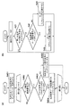
[装置の構成]
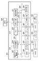
図1Aのブロック図により情報処理装置200の構成例を示す。情報処理装置200は、コンピュータ装置であり、データ転送を司るバスシステム30を有する。バスシステム30には、プロセッサとして複数のCPU10と11、ディジタル信号プロセッサ(DSP)12、および、グラフィカルプロセッサ(GPU)13などが接続される。
[Device configuration]
A configuration example of the
さらに、バスシステム30には、データ転送コントローラとして複数のDMAC14と15、および、メモリコントローラ(MEMC)20などが接続される。バスシステム30には、図示しない周辺機器を接続するための例えばPCIエクスプレスコントローラ(PCIe)21およびUSBコントローラ22などが接続される。バスシステム30には、メモリとしてリードオンリメモリ(ROM)23およびスタティックランダムアクセスメモリ(SRAM)24などが接続される。バスシステム30には、電力制御モジュール25が接続される。
Further, a plurality of
MEMC20は、情報処理装置200の外部のダイナミックランダムアクセスメモリ(DRAM)600に接続されている。CPU10は、DRAM600をワークメモリとして、ROM23に格納されたプログラムを実行する。図1Aに示す情報処理装置200の構成は、システムオンチップとよばれる半導体装置に代表的な構成であり、データ転送を司るバスシステム30は、インターコネクト、ファブリック、オンチップネットワークまたはネットワークオンチップと呼ばれる。
The MEMC20 is connected to a dynamic random access memory (DRAM) 600 outside the
なお、CPU10と11、DSP12、GPU13、DMAC14と15は、データ転送要求を発行するモジュール群であり、以下では「マスタモジュール」300と総称する場合がある。一方、MEMC20、PCIe21、USB22、ROM23、SRAM24、電力制御モジュール25は、データ転送要求を受信した後に応答するモジュール群であり、以下では「スレーブモジュール」400と総称する場合がある。なお、データ転送要求の発行と応答の両方の機能を有するモジュールも存在するが、図1Aには示さない。
Note that
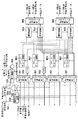
図1Bのブロック図により情報処理装置201の構成例を示す。情報処理装置201は、バスシステム230と割込制御部218を中心とするディジタルカメラシステム用のシステムオンチップ(SoC)とよばれる半導体装置に代表される構成を有する。なお、SoC内部には各モジュールに供給されるクロック信号を生成するクロックジェネレータやリセット信号を生成するリセットジェネレータなどが存在するが、図1Bにおいては、それらを省略する。
A configuration example of the
情報処理装置201は、データ転送を司るバスシステム230を有す。バスシステム230は、インターコネクト、ファブリック、オンチップネットワークまたはネットワークオンチップと呼ばれる。バスシステム230には、データ転送要求を発行するマスタモジュール300として、情報処理装置201全般の処理を行うCPU210が存在する。
The
さらに、バスシステム230には、マスタモジュール300として、動画処理部211、映像入力部212、映像出力部214、メモリカードコントローラ221、USBコントローラ222が存在する。動画処理部211は、撮影された静止画や動画を圧縮加工する。映像入力部212は、外部のCMOSセンサ605からディジタルデータに変換された映像データを入力し、映像データをMEMC220を介して外部のDRAM600へ転送する。
Further, the
映像出力部214は、DRAM600に格納された映像データをMEMC220を介して外部の表示デバイス604に転送する。メモリカードコントローラ221は、撮影された静止画や動画を外部のメモリカード601に転送するためのモジュールである。USBコントローラ222は、撮影された静止画や動画をUSBなどのシリアルバスを介して外部のUSBデバイス602にへ転送するためのモジュールである。
The video output unit 214 transfers the video data stored in the
また、バスシステム230には、データ転送要求を受信した後に応答するスレーブモジュール400として、操作ボタン制御部217、割込制御部218、MEMC220、ROMコントローラ223、電力制御モジュール225が存在する。操作ボタン制御部217は、ディジタルカメラ本体にあるボタンの操作を検出し、ボタン操作検出割込信号216を出力する。電力制御モジュール225は、バスシステム230の省電力制御を担い、省電力効果減少割込信号213を出力する。
Further, the
割込制御部218は、操作ボタン制御部217のボタン操作検出割込信号216、映像入力部212のビデオ垂直同期割込信号215、または、電力制御モジュール225の省電力効果減少割込信号213を受信し、割込信号219をCPU210に出力する。また、MEMC220は、外部のDRAM600との間でデータの転送を行う。ROMコントローラ223は、プログラムコードが格納された外部のROM603からデータを読み出す。なお、ROM603は、EEPROMなどの記録媒体である。
The interrupt
なお、図1Aと同様に、データ転送要求の発行と応答の両方の機能を有するモジュールも存在するが、図1Bには示さない。また、図1Aと図1Bにおいて同じ名称の構成は同じ機能を果たす。例えば、図1Aと図1Bにおいて、CPU10と210、バスシステム30と230、電力制御モジュール25と225などは同じ機能を果たす。以下では、同じ機能を果たす構成について、何れか一方の符号を用いて説明を行う。
Similar to FIG. 1A, there is a module having both functions of issuing and responding to a data transfer request, but it is not shown in FIG. 1B. Also, configurations with the same name in FIGS. 1A and 1B perform the same function. For example, in FIGS. 1A and 1B,
[バスシステムと電力制御モジュール]
図2A、図2Bのブロック図によりバスシステム30と電力制御モジュール25の構成例を示す。バスシステム30に接続されるマスタモジュール300とスレーブモジュール400の増加に伴い、バスシステム30は、近年、複数のデータ転送を司るデータ転送装置(以下、バスモジュール)100によって構成される。このような構成は、物理的なタイミング収束性の観点からである。また、各バスモジュール100は、データ転送検出モジュール101を有する。
[Bus system and power control module]
The block diagrams of FIGS. 2A and 2B show configuration examples of the
図3によりデータ転送を説明する。データ転送要求信号とデータ転送受信準備信号の二線ハンドシェイクプロトコルによって、データが転送される。データを送信するモジュール(以下、送信モジュール)はデータ転送要求信号と転送データの信号線を駆動し、データを受信するモジュール(以下、受信モジュール)はデータ転送受信準備信号を駆動する。そして、データ転送要求信号とデータ転送受信準備信号がともにアクティブの際にデータ転送が成立する。なお、データ転送要求信号とデータ転送受信準備信号はHレベルでアクティブ(ハイアクティブ)である。 Data transfer will be described with reference to FIG. Data is transferred by a two-wire handshake protocol of a data transfer request signal and a data transfer reception preparation signal. A module that transmits data (hereinafter, transmission module) drives a data transfer request signal and a signal line of transfer data, and a module that receives data (hereinafter, reception module) drives a data transfer reception preparation signal. Then, the data transfer is established when both the data transfer request signal and the data transfer reception preparation signal are active. The data transfer request signal and the data transfer reception preparation signal are active (highly active) at the H level.
各バスモジュール100は、詳細は後述するが、一つの電力制御インタフェイス(以下、電力制御I/F)と、複数のデータ転送インタフェイス(以下、データ転送I/F)を有する。バスモジュール100は、データ転送I/Fを介してマスタモジュール300、スレーブモジュール400、他のバスモジュール100に接続され、電力制御I/Fを介して電力制御モジュール25に接続される。また、図2Bに示すように、CPU10からの指示を受けて電力制御モジュール25に設定値に関する情報を通知する設定レジスタ800が存在する。具体的にどのような情報を電力制御モジュール25に提供するか、また、電力制御モジュール25の内部の構成については後述する。
Although the details will be described later, each
詳細は後述するが、各バスモジュール100と電力制御モジュール25の間では、電力制御I/Fを介して省電力モード移行要求信号、省電力モード応答信号および省電力モード許可信号の三つの電力制御信号の通信が行われる。ただし、省電力モード許可信号は、各バスモジュール100からデータ転送検出モジュール101を介して電力制御モジュール25に送信される。
Although the details will be described later, between each
電力制御モジュール25は、省電力モードへの移行を要求する省電力モード移行要求信号を出力し、バスモジュール100は省電力モード応答信号を出力する。省電力モードへの移行の可否を示す省電力モード許可信号は、バスモジュール100の出力信号とデータ転送検出モジュール101の検出結果の論理和信号である。なお、電力制御信号はLレベルでアクティブ(ローアクティブ)とする。
The
省電力モードにおいて、バスモジュール100の電源やクロックは停止または変更された状態にある。一方、データ転送検出モジュール101は、バスモジュール100の一部として機能するが、その電源はバスモジュール100から独立していて、バスモジュール100が省電力モードか否かに関わらず、省電力モード許可信号の状態を設定可能である。
In the power saving mode, the power supply and clock of the
図4のブロック図によりバスモジュール100とデータ転送検出モジュール101の構成例を示す。バスモジュール100は、転送データを受信する複数のスレーブデータ転送制御I/F501、転送データを後段に送信する複数のマスタデータ転送制御I/F506、および、電力制御I/F500を有する。なお、スレーブデータ転送制御I/F501によって受信されたデータは、ファーストインファーストアウトメモリ(FIFO)502に格納される場合がある。
The block diagram of FIG. 4 shows a configuration example of the
アドレスデコード回路503は、スレーブデータ転送制御I/F501またはFIFO502から出力されたデータの転送先を解析し、データ転送要求を転送先に対応する調停回路504に送信する。調停回路504は、データ転送要求の一つを選択する調停を行い、調停結果を選択回路505とマスタデータ転送制御I/F506に出力する。
The
選択回路505は、調停結果に基づき転送データを選択し、選択した転送データをマスタデータ転送制御I/F506に出力する。マスタデータ転送制御I/F506は、調停結果と選択された転送データを受信し、後段のバスモジュール100またはスレーブモジュール400との間でデータの送受信を行う。
The
一方、電力制御I/F500は、電力制御モジュール25から省電力モード移行要求信号を受信すると、省電力モードへの移行を示すために、非アクティブのデータ転送受信準備信号を各スレーブデータ転送制御I/F501に出力する。スレーブデータ転送制御I/F501は、データ転送受信準備信号を前段の送信モジュール(マスタモジュール300またはバスモジュール100)に出力して、新たに転送データを受信しない状態(以下、非受信状態)に移行する。
On the other hand, when the power control I / F500 receives the power saving mode transition request signal from the
次に、電力制御I/F500は、バスモジュール100内の処理状態を検出し、処理中を検出すると、省電力モード応答信号をHレベル(非アクティブ)に維持する。電力制御I/F500は、例えば、FIFO502の空状態に関する情報や、転送データのアウトスタンディング数(スレーブモジュール400のレスポンス状況管理)に関する情報などを用いて、バスモジュール100内の処理状態を判定する。
Next, the power control I /
図4には一部の転送データしか示さないが、実際の転送データにはアドレスデータ、ライトデータ、リードデータおよびレスポンスデータが含まれ、別々の回路を介して転送される。アドレスデータとライトデータに関して、マスタモジュール300またはバスモジュール100がデータ転送要求信号の駆動モジュールである。一方、リードデータとレスポンスデータに関して、スレーブモジュール400またはバスモジュール100がデータ転送要求信号の駆動モジュールである。
Although only a part of the transfer data is shown in FIG. 4, the actual transfer data includes address data, write data, read data, and response data, and is transferred via separate circuits. Regarding address data and write data, the
データ転送検出モジュール101のORゲート102は、各スレーブデータ転送制御I/F501が受信するデータ転送要求信号を論理和した論理和信号103を出力する。ORゲート104は、論理和信号103と、バスモジュール100が電源遮断された場合にLレベルになる信号105を入力し、論理和信号103と信号105の論理和を省電力モード許可信号として出力する。
The OR
属性生成回路106は、すべてのスレーブデータ転送制御I/F501が受信するデータ転送要求信号と、当該データ転送要求信号の駆動モジュールを示すマスタIDを入力し、転送要求データ属性信号を出力する。
The
●省電力モード移行が許可される場合
図5により省電力モード移行が許可される場合の電力制御モジュール25とバスモジュール100の動作を説明する。電力制御モジュール25は、省電力モード移行のトリガを受信すると、省電力モード移行要求信号をアクティブにする(時刻T2)。
● When the transition to the power saving mode is permitted Fig. 5 describes the operation of the
バスモジュール100は、省電力モード移行要求信号のアクティブを検出すると(T3)、データ転送受信準備信号を非アクティブにし(T4)、非受信状態に移行して処理状態を検出する。バスモジュール100は、非処理中(転送データなし)を検出すると(T5)、信号105をLレベルにして省電力モード応答信号をアクティブにすることで(T5)、省電力モード応答信号をアクティブにする(T6)。
When the
図5の例では、データ転送要求信号が非アクティブであるから論理和信号103はLレベルになり、新規の転送データが存在しないことが示される。その結果、論理和信号103と信号105がともにLレベルであり、ORゲート104が出力する省電力モード許可信号は、時刻T5においてLレベル(アクティブ)になる。
In the example of FIG. 5, since the data transfer request signal is inactive, the OR signal 103 is at the L level, indicating that there is no new transfer data. As a result, both the OR signal 103 and the
電力制御モジュール25は、省電力モード応答信号のアクティブを検出すると(T7)、省電力モード許可信号を判定する。そして、省電力モード許可信号のアクティブを検出すると(T7)、バスモジュール100が省電力モードへの移行を許可したと判定して、バスモジュール100のクロックや電源を変更または遮断する(T8からT10)。
When the
次に、電力制御モジュール25は、通常動作モード移行のトリガを受信すると、バスモジュール100のクロックや電源を供給後、省電力モード移行要求信号を非アクティブにする(T11)。
Next, when the
バスモジュール100は、省電力モード移行要求信号の非アクティブを検出すると(T12)、信号105をHレベルにして省電力モード許可信号を非アクティブにする(T14)。そして、省電力モード応答信号を非アクティブにし(T15)、その後、データ転送受信準備信号をアクティブにし(T16)、非受信状態を解除して新たに転送データを受信する状態になる。
When the
●省電力モード移行が許可されない場合
図6により省電力モード移行が許可されない場合の電力制御モジュール25とバスモジュール100の動作を説明する。電力制御モジュール25は、省電力モード移行のトリガを受信すると、省電力モード移行要求信号をアクティブにする(時刻T2)。
● When the transition to the power saving mode is not permitted Fig. 6 describes the operation of the
バスモジュール100は、省電力モード移行要求信号のアクティブを検出すると(T3)、データ転送受信準備信号を非アクティブにして(T4)、非受信状態に移行して処理状態を検出する。バスモジュール100は、処理中(転送データあり)を検出すると(T5)、信号105をHレベルに維持して省電力許可信号のアクティブを維持し(T5)、省電力モード応答信号をアクティブにする(T6)。
When the
図6の例では、データ転送要求信号がアクティブであり、論理和信号103がHレベルであり、新規の転送データが存在することが示される。この例では、論理和信号103と信号105がともにHレベルであり、ORゲート104が出力する省電力モード許可信号は、時刻T5においてHレベル(非アクティブ)になる。その後、バスモジュール100の転送データの処理が完了(非処理中)して信号105がLレベルになっても、データ転送要求信号がアクティブであり、論理和信号103のHレベルが維持される限り、省電力モード許可信号は非アクティブである。
In the example of FIG. 6, it is shown that the data transfer request signal is active, the OR signal 103 is at H level, and there is new transfer data. In this example, both the OR signal 103 and the
電力制御モジュール25は、省電力モード応答信号のアクティブを検出すると(T7)、省電力モード許可信号を判定する。そして、省電力モード許可信号の非アクティブを検出すると(T7)、バスモジュール100が省電力モードへの移行を許可しないと判定して、省電力モード移行要求信号を非アクティブにして(T11)、省電力モード移行要求を解除する。
When the
バスモジュール100は、省電力モード移行要求信号の非アクティブを検出すると(T12)、省電力モード応答信号を非アクティブにする(T15)。そして、データ転送受信準備信号をアクティブにし(T16)、非受信状態を解除して転送データの処理を継続する。
When the
●省電力モード移行後に新規の転送データが発生した場合
図7により省電力モード移行後に新規データ転送が発生した場合の電力制御モジュール25とバスモジュール100の動作を説明する(時刻T2)。電力制御モジュール25は、省電力モード移行のトリガを受信すると、省電力モード移行要求信号をアクティブにする(T2)。
● When new transfer data occurs after the transition to the power saving mode Figure 7 describes the operation of the
バスモジュール100は、省電力モード移行要求信号のアクティブを検出すると(T3)、データ転送受信準備信号を非アクティブにし(T4)、非受信状態に移行して処理状態を検出する。バスモジュール100は、非処理中(転送データなし)を検出すると(T5)、信号105をLレベルにして省電力モード許可信号を非アクティブとすることで(T5)、省電力モード応答信号をアクティブにする(T6)。
When the
図7の例では、時刻T5において、データ転送要求信号が非アクティブであるから論理和信号103はLレベルになり、新規の転送データが存在しないことが示される。その結果、論理和信号103と信号105がともにLレベルであり、ORゲート104が出力する省電力モード許可信号は、時刻T5においてアクティブになる。
In the example of FIG. 7, at time T5, since the data transfer request signal is inactive, the OR signal 103 becomes the L level, indicating that there is no new transfer data. As a result, both the OR signal 103 and the
電力制御モジュール25は、省電力モード応答信号のアクティブを検出すると(T7)、省電力モード許可信号を判定する。そして、省電力モード許可信号のアクティブを検出すると(T7)、バスモジュール100が省電力モードへの移行を許可したと判定して、バスモジュール100のクロックや電源を変更または遮断する(T8からT10)。
When the
図7の例では、時刻T9において、新規の転送データが発生しデータ転送要求信号の状態が変化してアクティブになる。バスモジュール100は省電力モードにあるため、時刻T9において信号105はLレベルに維持されるが、データ転送検出モジュール101のORゲート102が出力する論理和信号103は、時刻T9においてHレベルになる。その結果、ORゲート104が出力する省電力モード許可信号は、時刻T9において非アクティブになる。
In the example of FIG. 7, at time T9, new transfer data is generated and the state of the data transfer request signal changes and becomes active. Since the
電力制御モジュール25は、受信中の省電力モード許可信号の非アクティブを検出すると(T10)、バスモジュール100の省電力モードの解除が必要と判定する。そして、バスモジュール100のクロックや電源を供給後、省電力モード移行要求信号を非アクティブにする(T11)。
When the
バスモジュール100は、省電力モード移行要求信号の非アクティブを検出すると(T12)、省電力モード応答信号を非アクティブにする(T15)。そして、データ転送受信準備信号をアクティブにし(T16)、非受信状態を解除して新規の転送データの受信を開始する。
When the
図5から図7に示す電力制御モジュール25とバスモジュール100の動作により、複数のバスモジュール100を有するバスシステム30における転送データのロスやフリーズを回避して、省電力モードと通常動作モードの移行が実現される。
By operating the
●電力制御モジュール
図2Aに示すように、電力制御モジュール25は、各バスモジュール100に対応する電力制御I/Fを有する。各電力制御I/Fは、省電力モードの移行と復帰を制御する制御モジュール250、インターバルタイマ251、時間設定値最適化のためのタイマ値最適化モジュール252を有し、対応するバスモジュール100の状態を管理する。
● Power control module As shown in Fig. 2A, the
各制御モジュール250は、インターバルタイマ251に接続する簡易な専用回路、または、プログラマブルロジックデバイス(PLD)などによって実現される。あるいは、電力制御モジュール25のCPUが電力制御モジュール25のROMなどに格納されたプログラムを実行することによって実現されてもよい。
Each
図8Aのフローチャートにより制御モジュール250の処理を説明する。電力制御モジュール25が動作を開始すると、制御モジュール250は、バスモジュール100に電源とクロックを供給してバスモジュール100を通常動作モードにする(S11)。その際、省電力モード移行要求信号は非アクティブである。
The processing of the
次に、制御モジュール250は、省電力モード移行のトリガを受信したか否かを判定し(S12)、未受信の場合は処理をステップS11に戻して、バスモジュール100の通常動作モードを維持する。なお、省電力モード移行のトリガは、CPU10や11によるレジスタアクセスや割込み、外部イベントなどである。
Next, the
省電力モード移行のトリガを受信すると、制御モジュール250は、インターバルタイマ251のカウント値countを判定する(S13)。カウント値count>0の場合、制御モジュール250は、インターバルタイマ251のカウント値countをデクリメントして(S14)、処理をステップS13に戻す。
Upon receiving the power saving mode transition trigger, the
インターバルタイマ251のカウント値count=0になると、制御モジュール250は、省電力モード移行要求信号をアクティブにして(S15)、バスモジュール100が省電力モードへの移行を許可するか否かを判定する。つまり、省電力モード応答信号の判定(S16)と省電力モード許可信号の判定(S17)を行う。
When the count value of the
省電力モード応答信号がアクティブになり(S16)、省電力モード許可信号がアクティブになった(S17)場合、制御モジュール250は、バスモジュール100が省電力モードへの移行を許可したと判定する。そして、バスモジュール100の電源やクロックを制御する(S18)。なお、省電力モードから通常動作モードへの復帰時間や応答性能を考慮して、電源の遮断、クロックの遮断、クロック速度の変更などが行われる。その後、制御モジュール250は、処理をステップS19に進めて、バスモジュール100の通常動作モードへの復帰トリガを待つ状態になる。
When the power saving mode response signal becomes active (S16) and the power saving mode permission signal becomes active (S17), the
バスモジュール100を省電力モードへ移行させた後、制御モジュール250は、通常動作モードへの復帰トリガを受信したか否かを判定する(S19)。復帰トリガには幾つかの種類が存在し、CPU10や11によるレジスタアクセスや割込み、外部イベントなどである。また、新規の転送データが発生した場合、バスモジュール100が省電力モードにあるため、データ転送検出モジュール101によって省電力モード許可信号が非アクティブになるが、これも復帰トリガの一つである。復帰トリガを受信すると、制御モジュール250は、処理をステップS20に進める。
After shifting the
一方、省電力モード応答信号がアクティブになったが(S16)、省電力モード許可信号が非アクティブ(S17)の場合、制御モジュール250は、バスモジュール100が省電力モードへの移行を許可しないと判定して、処理をステップS20に進める。バスモジュール100に処理中の転送データ転送が存在したり、新規の転送データが存在する場合、バスモジュール100は、転送データのロスやフリーズを避けるために、省電力モードへの移行を許可しない。
On the other hand, if the power saving mode response signal is activated (S16) but the power saving mode permission signal is inactive (S17), the
復帰トリガを受信した場合、または、省電力モードへの移行が不可能な場合、制御モジュール250は、省電力モード移行要求を解除し、バスモジュール100に電源やクロックが供給されていない場合は電源やクロックの供給を再開する(S20)。つまり。なお、電源遮断から復帰させる場合は、電源が安定した後にバスモジュール100のリセット処理が行われる。その後、制御モジュール250は、省電力モード移行要求信号を非アクティブにし、省電力モード応答信号が非アクティブになったことを確認した後、処理をステップS21に進める。
When a return trigger is received, or when the transition to the power saving mode is not possible, the
次に、制御モジュール250は、再び省電力モード移行要求を発行するか否かを判定し(S21)、省電力モード移行要求を発行しない場合は処理をステップS12に戻す。また、省電力モード移行要求を発行する場合は、インターバルタイマ2001のカウント値countに所定のリファレンス値を設定し(S22)、処理をステップS13に戻す。
Next, the
制御モジュール250による上記処理により、CPU10などのマスタモジュール300による電力制御に関わる手続を軽減することが可能になる。
The above processing by the
●タイマ値最適化モジュール
タイマ値最適化モジュール252は、予め決められたルールに基づいてタイマ値を動的に変更し、最適なタイマ値に調整するモジュールである。図8Bのフローチャートによりタイマ値最適化モジュール252の動作を含む制御モジュール250の処理を説明する。なお、図8Bにおいて、図8Aと同様の処理には同一符号を付し、その詳細説明を省略する。
● Timer value optimization module The timer
電力制御モジュール25が動作を開始すると、制御モジュール250は、バスモジュール100に電源とクロックを供給してバスモジュール100を通常動作モードにする(S11)。その際、省電力モード移行要求信号は非アクティブである。
When the
次に、制御モジュール250は、省電力モード移行要求を発行するか否かを判定し(S31)、省電力モード移行要求を発行しない場合は処理をステップS11に戻して、バスモジュール100の通常動作モードを維持する。省電力モード移行要求を発行するか否かの判定は、CPU10によるレジスタアクセスや割り込み、外部イベントなどの外部トリガに基づいて判定される場合と、制御モジュール250が自身の内部的な状態に基づいて自律的に判定する場合がある。
Next, the
制御モジュール250は、省電力モード移行要求を発行する場合、インターバルタイマ251のカウント値countにタイマ値最適化モジュール252から通知される所定のリファレンス値(時間設定値)を設定する(S32)。そして、制御モジュール250は、インターバルタイマ251のカウント値countの判定(S14)から省電力モード移行要求の解除(S20)を実行するが、それらの処理は図8Aの場合と同じであり、詳細説明を省略する。なお、図8Bの処理においては、図8Aの処理と異なり、省電力モード移行要求の解除(S20)の後、処理はステップS11に戻る。
When issuing a power saving mode transition request, the
タイマ値最適化モジュール252を含む制御モジュール250による上記処理により、CPU10などのマスタモジュール300による電力制御に関わる手続を軽減することが可能になる。
The above processing by the
●インターバルタイマのカウント値
図9により電力制御信号とインターバルタイマ251のカウント値countの関係を説明する。
● Count value of interval timer Fig. 9 explains the relationship between the power control signal and the count value count of the
省電力モード移行要求信号がアクティブになった後、省電力モード応答信号がアクティブになるが省電力モード許可信号がアクティブにならない状況は、上述したように、バスモジュール100が省電力モードへの移行を許可しない場合である。この場合、電力制御モジュール25は、省電力モード移行要求信号が非アクティブにし、インターバルタイマ251に設定した時間が経過した後、再び省電力モード移行要求信号をアクティブにする。つまり、電力制御モジュール25は、CPU10や11の介在なしにインターバルタイマ251に設定した間隔で省電力モード移行要求を行う。
In the situation where the power saving mode response signal becomes active but the power saving mode permission signal does not become active after the power saving mode transition request signal becomes active, the
バスモジュール100は、データのロスやフリーズを避けるためのモード移行期間において、省電力モードへの移行が可能か否かを判定し、移行が可能であればその旨を電力制御モジュール25に通知する。電力制御モジュール25は、省電力モードへの移行が可能な状況においてのみ、電源やクロックを制御することができ、バスモジュール100の省電力化を行うことができる。
The
電力制御モジュール25は、複数のバスモジュール100に対応して複数のインターバルタイマ251を有する。各インターバルタイマ251の値は、制御対象のバスモジュール100の転送性能要求に従い事前に設定される。転送帯域要求が低いなどデータ転送能力が低いバスモジュール100に対応するインターバルタイマ251には低めの値を設定し、省電力モードへの移行の機会を増やす。
The
一方、転送帯域要求が高いバスモジュール100に対応するインターバルタイマ251には高めの値を設定し、省電力モード移行期間による実効性能の低下の機会を減らす。同様に、インターバルタイマ251の値は、転送帯域の要求だけでなく、転送レイテンシの要求を考慮して設定することも考えられる。つまり、各バスモジュール100の使用条件を考慮して、転送の実効性能と電力消費の最適なバランスを得ることが可能になる。
On the other hand, a higher value is set for the
上記のようにインターバルタイマ251への入力値を適切にするために、電力制御モジュール25内部に配置したタイマ値最適化モジュール252によりインターバルタイマ251のタイマ設定値を動的に変更する。そして、判定指標としての省電力効果の高いタイマ設定値を探索する。
In order to make the input value to the
例えば、後述する例においては、ディジタルカメラシステム用の情報処理装置201が動画撮影などの処理を行っている間に、各インターバルタイマ251に設定すべきタイマ設定値が、タイマ値最適化モジュール252により自動的に調整される。こうすることで、ディジタルカメラシステム用の情報処理装置201の動画撮影モードや操作待ち状態などの各機器状態に応じて、省電力効果が高い最適なタイマ値を自動的に調整することができる。
For example, in the example described later, the timer setting value to be set in each
[タイマ値最適化モジュール]
タイマ値最適化モジュール252は、インターバルタイマ251のタイマ設定値を動的に変更し、省電力効果が高いタイマ設定値を探索、判定する。探索完了後、その判定結果として最も省電力効果が高い最適なタイマ設定値をインターバルタイマ251に入力するためのモジュールである。
[Timer value optimization module]
The timer
図10のブロック図によりタイマ値最適化モジュール252の内部構成例を示す。タイマ値最適化モジュール252は、タイマ値調整モジュール255、最適タイマ値判定モジュール256、最適タイマ値格納モジュール257、タイマ値切替モジュール258を有する。
An example of the internal configuration of the timer
これらモジュールの入出力信号として、タイマ値調整モード選択信号253、タイマ値更新トリガ信号254、タイマ値調整用パラメータ270、最適タイマ値省電力効果測定信号2563が存在する。また、調整用タイマ値259、更新用最適タイマ値260、格納済み最適タイマ値261、固定タイマ値設定信号269、省電力効果減少割込信号213、バス使用状態信号262、クロックオンオフ信号263が存在する。
As input / output signals of these modules, there are a timer value adjustment
以下、タイマ値最適化モジュール252の詳細を説明する。CPU10は、タイマ値調整を行うか否かをタイマ値調整モード選択信号253により選択し、タイマ値調整モジュール255、最適タイマ値判定モジュール256、タイマ値切替モジュール258に通知する。タイマ値調整モード選択信号253は、値が‘1’の場合にタイマ値調整モードを示し、値が‘0’の場合に調整後タイマ値使用モードを示す。
The details of the timer
タイマ値調整モードの場合はタイマ値調整モジュール255が出力する調整用タイマ値259が選択され、調整後タイマ値使用モードの場合は最適タイマ値格納モジュール257が出力する格納済み最適タイマ値261が選択される。そして、選択されたタイマ値が、タイマ値切替モジュール258を介してタイマ設定値として外部のインターバルタイマ251へ送られる。
In the timer value adjustment mode, the
タイマ値更新トリガ信号254は、CPU10により制御され、調整用タイマ値の更新タイミングをタイマ値調整モジュール255および最適タイマ値判定モジュール256に通知する。本実施例ではタイマ値更新トリガ信号254の出力を1サイクルのパルス信号とし、1で調整用タイマ値の更新タイミングを示す。
The timer value
調整用タイマ値259は、タイマ値調整モジュール255の出力信号であり、その動作は後述するタイマ値調整モジュール255の動作説明において行う。更新用最適タイマ値260は、最適タイマ値判定モジュール256の出力信号であり、その動作は後述する最適タイマ値判定モジュール256の動作説明において行う。格納済み最適タイマ値261は、最適タイマ値格納モジュール257の出力信号であり、その動作は後述する最適タイマ値格納モジュール257の動作説明において行う。
The
バス使用状態信号262は、制御モジュール250とバスモジュール100間で使用される電力制御信号(省電力モード移行要求信号、省電力モード応答信号、省電力モード許可信号)などを含む信号である。また、バスモジュール100のハンドシェイク制御信号(データ転送要求信号、データ転送受信準備信号)などを含む信号であり、その詳細動作は図5、図6、図7において説明される。
The bus
クロックオンオフ信号263は、制御モジュール250がバスモジュール100のクロックの供給・停止を制御するための信号である。クロックジェネレータ(不図示)から生成されるクロック信号をこのクロックオンオフ信号263によりマスクするようなクロックゲーティング回路(不図示)を介してバスモジュール100のクロックポートに供給されることになる。
The clock on / off
タイマ値調整モジュール255は、タイマ値調整モード選択信号253によって指示されるタイマ値調整モードにおいて、タイマ値更新トリガ信号254がアクティブの際に調整用タイマ値を自動的に更新し、インターバルタイマ251へ出力する。その際のタイマ値の更新方法は、入力されるタイマ値調整用パラメータ(時間設定値の調整用パラメータ)270に従う。
The timer
本実施例では、タイマ値調整用パラメータ270として開始タイマ値、ステップ値(初期設定値)、タイマ更新数(更新回数)の三つのパラメータを使用する。インターバルタイマ251へ出力される調整用タイマ値は、タイマ値更新トリガ信号254の入力ごとに更新される。更新ルールは以下のようになる。
if (一回目のタイマ値更新トリガの入力)
調整用タイマ値 = 開始タイマ値;
if (二回目のタイマ値更新トリガの入力)
調整用タイマ値 = 開始タイマ値 + ステップ値×1;
if (三回目のタイマ値更新トリガの入力)
調整用タイマ値 = 開始タイマ値 + ステップ値×2;
:
:
if (N回目のタイマ値更新トリガの入力)
調整用タイマ値 = 開始タイマ値 + ステップ値×(N-1);
In this embodiment, three parameters of the start timer value, the step value (initial setting value), and the timer update number (update count) are used as the timer
if (input of the first timer value update trigger)
Adjustment timer value = Start timer value;
if (input of the second timer value update trigger)
Adjustment timer value = start timer value + step value x 1;
if (input of the third timer value update trigger)
Adjustment timer value = start timer value + step value x 2;
:
:
if (input of Nth timer value update trigger)
Adjustment timer value = Start timer value + Step value x (N-1);
ただし、上記の調整用タイマ値の調整方法は一例であり、さらにインテリジェントに調整用タイマ値の最適値を探索する方法を採ることも考えられる。また、調整用タイマ値の具体的な使用例は後述する。 However, the above adjustment method of the adjustment timer value is an example, and it is also conceivable to adopt a method of intelligently searching for the optimum value of the adjustment timer value. A specific example of using the adjustment timer value will be described later.
上記では、タイマ値調整用パラメータ270を外部から入力し、タイマ値調整モジュール255がこのパラメータに応じて調整用タイマ値を更新する例を説明した。しかし、別の手段として、タイマ値更新トリガ254とともに外部モジュールから調整用タイマ値そのものが入力されるケースも考えられる。
In the above, an example in which the timer
タイマ値調整モジュール255の出力である調整用タイマ値259は、タイマ値調整モード選択信号253によりタイマ値調整モードが選択されると、インターバルタイマ251のタイマ設定値として使用される。それと同時に、調整用タイマ値259は、最適タイマ値判定モジュール256に通知される。
The
最適タイマ値判定モジュール256は、タイマ値調整モード選択信号253が示すタイマ値調整モードにおいて、タイマ値調整モジュール255が出力する調整用タイマ値ごとに、バスモジュール100の省電力効果を測定する。そして、タイマ値調整モードが終了した時点で、測定された省電力効果のうち、最も省電力効果の高い調整用タイマ値を判定し、その値を最適タイマ値格納モジュール257に格納する。バスモジュール100の省電力効果の測定は、バス使用状態信号262およびクロックオンオフ信号263の状態から、最適タイマ値判定モジュール256が行う。
The optimum timer
最適タイマ値格納モジュール257は、最も高い省電力効果が得られる最適タイマ値を格納し、タイマ値調整モード選択信号253が示す調整後タイマ値使用モードにおいて、格納された最適タイマ値をインターバルタイマ251に通知するモジュールである。
The optimum timer
最適タイマ値格納モジュール257は、タイマ値調整モード選択信号253により調整後タイマ値使用モードになった際に、最適タイマ値判定モジュールの出力結果を基に、格納している最適タイマ値を更新する。
The optimum timer
タイマ値切替モジュール258は、タイマ値調整モード選択信号253の出力に基づきタイマ値調整を実行する場合(信号値‘1’)は、タイマ値調整モジュール255の出力である調整用タイマ値259を選択する。また、タイマ値調整を実行しない場合(信号値‘0’)は、最適タイマ値格納モジュール257の出力である格納済み最適タイマ値261を選択し、インターバルタイマ251に出力する。
When the timer
また、タイマ値調整を行わない場合で、予め決められたタイマ設定値をインターバルタイマ251へ出力したい場合、固定タイマ値設定信号269を用いて最適タイマ値格納モジュール257内の最適タイマ値を書き換えることが可能である。固定タイマ値設定信号269は、固定タイマ設定値(不図示)と固定タイマ設定値の書込制御信号(不図示)によって構成される。固定タイマ設定値の書込制御信号がアクティブの場合、固定タイマ設定値が有効データとして扱われる。
If you do not want to adjust the timer value and want to output a predetermined timer setting value to the
また、図10に示す最適タイマ値省電力効果測定信号2563、および、省電力効果減少割込信号213の詳細については後述する。
The details of the optimum timer value power saving
●最適タイマ値判定モジュール
最適タイマ値判定モジュール256は、下式により、バスモジュール100の省電力効果の判定を行う。
省電力効果 = 省電力モード期間の総期間 - 省電力モード移行期間の総期間 …(1)
● Optimal timer value determination module The optimum timer
Power saving effect = Total period of power saving mode --Total period of power saving mode transition period… (1)
省電力モード期間はバスモジュール100のクロックが停止している期間であり、省電力モード移行期間はバスモジュール100に対し省電力モード移行要求が発行されているが、バスモジュール100のクロックが停止していない期間である。従って、式(1)の計算結果が大きいと省電力効果が高いということになる。また、式(1)の計算結果は負値をとることもあり得る。また、式(1)に示す省電力効果の計算式は一例であり、その他の計算方法も考えられる。
The power saving mode period is the period during which the clock of the
省電力モード移行は、以下の三種類が存在する。一つ目は、通常動作モードから省電力モードへのモード移行(図7のケースのうち最初のモード移行に相当)である。二つ目は、省電力モードから通常動作モードへのモード移行(図7のケースのうち二番目のモード移行に相当)である。三つ目は、通常動作モード間の移行(図6のケースに相当)である。また、上記の「省電力モード移行期間」はそれぞれのモード移行期間の総和を意味する。 There are the following three types of power saving mode transition. The first is the mode transition from the normal operation mode to the power saving mode (corresponding to the first mode transition in the case of FIG. 7). The second is the mode transition from the power saving mode to the normal operation mode (corresponding to the second mode transition in the case of FIG. 7). The third is the transition between normal operation modes (corresponding to the case in FIG. 6). Further, the above-mentioned "power saving mode transition period" means the total of each mode transition period.
図11のブロック図により最適タイマ値判定モジュール256の構成例を示す。最適タイマ値判定モジュール256は、省電力モード期間測定モジュール2560、省電力モード移行期間測定モジュール2561、省電力効果測定・最適タイマ値判定モジュール2562を有する。以下、これらモジュールの動作の詳細を説明する。
The block diagram of FIG. 11 shows a configuration example of the optimum timer
省電力モード期間測定モジュール2560は、カウンタ(省電力モード期間カウンタ)で構成されている。そして、タイマ値調整モード選択信号253によって通知されるタイマ値調整モードの期間中、省電力モード期間の総和を測定し、測定結果を「省電力モード期間の総期間」として省電力効果測定・最適タイマ値判定モジュール2562に通知する。
The power saving mode
省電力モード移行期間測定モジュール2561は、カウンタ(省電力モード移行期間カウンタ)で構成されている。そして、タイマ値調整モード選択信号253によって通知されるタイマ値調整モードの期間中、省電力モード移行期間の総和を測定し、測定結果を「省電力モード移行期間の総期間」として省電力効果測定・最適タイマ値判定モジュール2562に通知する。
The power saving mode transition
省電力効果測定・最適タイマ値判定モジュール2562は、タイマ値調整モード選択信号253によって通知されるタイマ値調整モードの終了後、次の動作を行う。省電力モード期間測定モジュール2560から通知されたカウント値(省電力モード期間の総期間)から省電力モード移行期間測定モジュール2561から通知されたカウンタ値(省電力モード移行期間の総期間)を減算する。そして、計算結果の値をタイマ値更新トリガ254に同期してラッチし、省電力効果を示す省電力効果判定信号として扱う。なお、図11には省電力効果判定信号を示さないが、後述する図12に波形として記載する。
The power saving effect measurement / optimum timer
省電力効果測定・最適タイマ値判定モジュール2562は、タイマ値調整モード選択信号253がアクティブとなっていた期間中の調整用タイマ値259ごとの省電力効果判定信号の値を比較する。そして、比較の結果、省電力効果判定信号の値が最も高くなる調整用タイマ値259を省電力効果が最も高い最適なタイマ値として最適タイマ値格納モジュール257に格納する。
The power saving effect measurement / optimum timer
省電力効果測定・最適タイマ値判定モジュール2562は、タイマ値調整モード期間中の調整用タイマ値259と省電力効果判定信号を記憶し、省電力効果が最大の調整用タイマ値259をモジュール外部へ出力する。しかし、そのための回路構成方法を限定するものではない。
The power saving effect measurement / optimum timer
例えば、タイマ値調整モード期間中の調整用タイマ値259とその省電力効果判定信号を記憶し、当モードが終了した際に、省電力効果が最も高い調整用タイマ値259をセレクタで出力するような構成が考えられる。ただし、この構成は、調整用タイマ値259が多ければ多いほど、それを記憶するために回路規模が増大すると考えられる。
For example, the
別の構成として、直近の省電力効果判定信号の値が最も大きい調整用タイマ値259と省電力効果判定信号だけを一時的に記憶する構成が考えられる。この場合、タイマ値更新トリガ信号254が入力される度に、次の動作を行う。最新の調整用タイマ値259の省電力効果判定信号と、記憶されている直近までで最も値が大きい省電力効果判定信号の大小を比較する。そして、最新の省電力効果判定信号の値が大きい場合は、記憶する調整用タイマ値259と省電力効果判定信号を、最新の調整用タイマ値259と省電力効果判定信号に更新する。
As another configuration, a configuration is conceivable in which only the
●最適タイマ値省電力効果測定信号と省電力効果減少割込信号
最適タイマ値省電力効果測定は、タイマ値調整モード選択信号253が非アクティブ(調整後タイマ値使用モード)の場合に使用される機能である。最適タイマ値省電力効果測定信号2563が‘1’の場合、省電力モード期間測定モジュール2560、省電力モード移行期間測定モジュール2561、省電力効果測定・最適タイマ値判定モジュール2562が動作し、省電力効果の測定が行われる。これにより、タイマ値調整モード選択信号253が非アクティブの場合も、タイマ値更新トリガ信号254の入力ごとに省電力効果が計算される。ただし、このとき使用されるタイマ設定値は、既に決まっている最適タイマ値であり、最適タイマ値におけるタイマ値更新トリガ信号254の入力ごとの省電力効果が計算されることになる。
● Optimal timer value power saving effect measurement signal and power saving effect reduction interrupt signal Optimal timer value power saving effect measurement is used when the timer value adjustment
省電力効果測定・最適タイマ値判定モジュール2562は、タイマ値調整モード時の最適タイマ値における省電力効果の値を記憶する。そして、調整後タイマ値使用モードに移行した後、継続して測定される最適タイマ値における省電力効果の値(測定値)と、記憶する省電力効果の値(記憶値)を比較して、記憶値に対して測定値が半減した場合に省電力効果減少割込信号213をアサートする。なお、省電力効果減少割込信号213のアサートは省電力効果が半減した場合に限らず、予め閾値を設定し、測定値が記憶値の閾値未満(例えば70%未満)になると省電力効果減少割込信号213のアサートするようにしてもよい。また、省電力効果減少割込信号213を使用例については後述する。
The power saving effect measurement / optimum timer
●省電力効果の測定方法
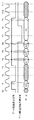
図12A、図12Bにより省電力効果の測定方法を説明する。タイマ値調整モード選択信号253がアサートされている(信号レベルH)期間、インターバルタイマ251は、定期的に省電力モード移行要求信号をアサート(信号レベルL)する。そして、省電力モードに入っている時間(省電力モード期間)と、モード移行の際に無駄にクロックが供給されている時間(省電力モード移行期間)をカウントする。その後、両者のカウンタの演算結果から省電力効果を算出する。図12A、図12Bは上記のシーケンスを示している。
● Measurement method of power saving effect The measurement method of power saving effect is explained with reference to FIGS. 12A and 12B. During the period when the timer value adjustment
CPU10は、タイマ値調整を開始するため、タイマ値調整モード選択信号253をアクティブ(信号レベルL)にする(時刻T0)。タイマ値調整モード選択信号253はレベル信号であり、時刻T0からCPU10がタイマ値調整モードの完了を指示するまでの期間(不図示)、常にアクティブに固定される。この期間、タイマ値切替モジュール258は、タイマ値調整モジュール255からの調整用タイマ値をインターバルタイマ251に選択的に出力する。
The
また、CPU10は、タイマ値更新トリガ信号254をアクティブにすると同時に、これに同期した調整用タイマ値259をタイマ値調整モジュール255に設定することで、調整用タイマ値259の更新を通知する。図12A、図12Bの例では、最初のタイマ調整時の調整用タイマ値259は「2」、二回目のタイマ調整時の調整用タイマ値259は「4」を仮定している。このとき、インターバルタイマ251には調整用タイマ値259がロードされ、以後「0」になるまで毎サイクルカウントダウンされることになる。
Further, the
CPU10は、タイマ最適化モジュール252に通知するため、タイマ値更新トリガ信号254をアクティブにする(T1)。タイマ値更新トリガ信号254がアクティブになると、省電力モード期間測定モジュール2560の出力である省電力モード期間カウンタの値は0にリセットされる(T2)。同時に、省電力モード移行期間測定モジュール2561の出力である省電力モード移行期間カウンタの値は0にリセットされる(T2)。
The
調整用タイマ値259がロードされたインターバルタイマ251は、カウントダウンを開始し、カウント値が1になると、省電力モード移行要求信号をアクティブにする(T4)。バスモジュール100は、省電力モード移行要求信号のアクティブを検出すると(T5)、データ転送受信準備信号を非アクティブにし(T6)、非受信状態に移行して処理状態を検出する。
The
バスモジュール100は、非処理中(転送データなし)を検出すると(T6)、信号105をLレベルにして省電力モード許可信号をアクティブにすることで(T7)、省電力モード応答信号をアクティブにする(T8)。
When the
図12A、図12Bの例では、データ転送要求信号が非アクティブであるから論理和信号103はLレベルになり、新規の転送データが存在しないことが示される。その結果、論理和信号103と信号105がともにLレベルであり、ORゲート104が出力する省電力モード許可信号は、時刻T7においてLレベル(アクティブ)になる。
In the examples of FIGS. 12A and 12B, since the data transfer request signal is inactive, the OR signal 103 is at the L level, indicating that there is no new transfer data. As a result, both the OR signal 103 and the
電力制御モジュール25は、省電力モード応答信号のアクティブを検出すると(T9)、省電力モード許可信号を判定する。そして、省電力モード許可信号のアクティブを検出すると(T9)、バスモジュール100が省電力モードへの移行を許可したと判定して、クロックオンオフ信号263を非アクティブにして、クロック供給の停止を指示する(T9)。その後、クロックオンオフ信号263は85サイクルの期間(T9-T92)にわたり非アクティブとなり、その結果、85サイクルの期間(T10-T93)に亘りクロックが停止する。
When the
バスモジュールクロックは、クロックオンオフ信号263によりクロックの供給が制御される。クロックオンオフ信号263は、アクティブのときクロックが供給状態(オン)になり、非アクティブの時にクロックの供給が停止状態(オフ)になる信号である。バスモジュールクロックは、クロックゲーティング回路(不図示)により、クロックオンオフ信号263の変化の1サイクル後のタイミングでクロックのオンオフを制御するように構成されている。
The supply of the bus module clock is controlled by the clock on / off
省電力モード期間カウンタは、省電力モードに入ってクロックが停止している期間(クロックオンオフ信号263がLレベル)に、1サイクルにつき+1ずつインクリメントされ、それ以外は保持される。
The power saving mode period counter is incremented by +1 per cycle during the period when the clock is stopped in the power saving mode (clock on / off
省電力モード移行期間カウンタは、通常動作モードから省電力モードへのモード移行期間、1サイクルにつき+1ずつインクリメントされる。なお、当該モード移行期間は、省電力モード移行要求信号がアクティブになった時間から、省電力モード応答信号が非アクティブからアクティブに変化する時間までである。また、当該モード移行期間を除く期間、および、当該モード移行期間中においてもクロックオンオフ信号263が非アクティブの期間、省電力モード移行期間カウンタのカウント値は保持される。
The power saving mode transition period counter is incremented by +1 per cycle during the mode transition period from the normal operation mode to the power saving mode. The mode transition period is from the time when the power saving mode transition request signal is activated to the time when the power saving mode response signal changes from inactive to active. Further, the count value of the power saving mode transition period counter is retained during the period excluding the mode transition period, the period during which the clock on / off
次に、時刻T92において、新規の転送データが発生し、データ転送要求信号の状態が変化してアクティブになる。これを受けて、時刻T93においてクロックオンオフ信号263がアクティブになり、時刻T94からクロックの供給が再開される。
Next, at time T92, new transfer data is generated, and the state of the data transfer request signal changes and becomes active. In response to this, the clock on / off
バスモジュール100は、省電力モードにあるため、時刻T92において信号105はLレベルに維持されるが、データ転送検出モジュール101のORゲート102が出力する論理和信号103は時刻T92においてHレベルになる。その結果、ORゲート104が出力する省電力モード許可信号は、時刻T92において非アクティブになる。
Since the
電力制御モジュール25は、受信中の省電力モード許可信号の非アクティブを検出すると(T93)、バスモジュール100の省電力モードの解除が必要と判定する。そして、バスモジュール100のクロックや電源の供給再開後、省電力モード移行要求信号を非アクティブにする(T95)。
When the
バスモジュール100は、省電力モード移行要求信号の非アクティブを検出すると(T96)、省電力モード応答信号を非アクティブにする(T99)。その後、データ転送受信準備信号をアクティブにし(T100)、非受信状態を解除して新たに転送データを受信する状態になる。
When the
一回目の省電力モード移行要求が発行され、データ転送受信準備信号が一旦非アクティブになってから再度アクティブになった時点(T100)において、省電力モード期間カウンタの値は「84」であり、省電力モード移行期間カウンタの値は「11」である。 When the first power saving mode transition request is issued and the data transfer reception preparation signal is once deactivated and then reactivated (T100), the value of the power saving mode period counter is "84". The value of the power saving mode transition period counter is "11".
省電力モード移行要求信号を再びアクティブにし(T102)、転送受信準備信号が非アクティブになる(T104)。その結果、時刻T107において、省電力モード応答信号と省電力モード許可信号の双方がアクティブになる。ところが、時刻T107の時点では、データ転送要求信号がアクティブのため、電力制御モジュール25は省電力状態への移行はできないと判断する。そして、クロックオンオフ信号263を非アクティブのままにして、省電力モード移行要求信号を非アクティブとする(T111)。その結果、時刻T115において省電力モード応答信号が非アクティブになり、時刻T116においてデータ転送受信準備信号がアクティブになる。
The power saving mode transition request signal is activated again (T102), and the transfer reception preparation signal is deactivated (T104). As a result, at time T107, both the power saving mode response signal and the power saving mode permission signal become active. However, at time T107, since the data transfer request signal is active, the
このとき、時刻T102からT115までの二回目の省電力モード移行要求の期間において、クロックオンオフ信号263が非アクティブのままのため、省電力モード期間カウンタの値は「85」に保持される。一方、省電力モード移行期間カウンタは、時刻T103からT115までの期間、常に1サイクルにつき+1ずつインクリメントされて、時刻T115におけるカウント値は「25」になる。これは、二回目の省電力モード移行要求に対して省電力効果がなく、移行に関する処理サイクルのオーバヘッドが生じただけであることを意味する。
At this time, since the clock on / off
次に、CPU10が再度タイマ値更新トリガ信号254をアクティブにすると同時に、これに同期した調整用タイマ値259が設定される。このようにすることで、電力制御モジュール25は、新たな調整用タイマ値259をインターバルタイマ251に供給することで、省電力モード移行要求の発行を開始する。
Next, the
次に、CPU10が再度タイマ値更新トリガ信号254をアクティブにすると同時に、これに同期した調整用タイマ値259が設定される(T117)。同時に、省電力効果測定・最適タイマ値判定モジュール2562は、一回目のタイマ値調整の省電力効果を省電力モード期間カウンタと省電力モード移行期間カウンタから計算する。そして、計算値を省電力効果一時格納レジスタ(不図示)に省電力効果判定信号として格納する(T118)。同時に、その時の調整用タイマ値259を時間設定値一時格納用の調整用タイマ値一時格納レジスタ(不図示)に格納する。これらの一時格納レジスタは、省電力効果測定・最適タイマ値判定モジュール2562の内部レジスタである。省電力効果測定・最適タイマ値判定モジュール2562は、タイマ更新数分の内部レジスタを有し、省電力効果と対応する調整用タイマ値259を保持することができる。
Next, the
式(1)に示したように、省電力モード期間カウンタ値から省電力モード移行期間カウンタ値を減算した結果が省電力効果であり、上記の例では85-25=60が省電力効果判定信号の値になる。なお、省電力効果判定信号の値は、正の整数だけでなく、負の整数をとることも可能である。負の場合、省電力モードへの移行に要した時間の方がクロック停止して電力を抑えることができた時間よりも長く、省電力効果に乏しいことを意味する。 As shown in equation (1), the result of subtracting the power saving mode transition period counter value from the power saving mode period counter value is the power saving effect. In the above example, 85-25 = 60 is the power saving effect judgment signal. Becomes the value of. The value of the power saving effect determination signal can be a negative integer as well as a positive integer. If it is negative, it means that the time required to shift to the power saving mode is longer than the time required to stop the clock and suppress the power, and the power saving effect is poor.
また、図12A、図12Bには示さないが、CPU10は、タイマ値調整を完了する際に、タイマ値調整モード選択信号253を非アクティブにする。その後、省電力効果測定・最適タイマ値判定モジュール2562は、各調整用タイマ値に対する省電力効果一時格納レジスタの値の大小比較(省電力効果比較)を行う。そして、省電力効果一時格納レジスタに格納された省電力効果判定信号の最大値に対応する調整用タイマ値一時格納レジスタに格納された調整用タイマ値259を選択する。そして、選択した調整用タイマ値259を省電力効果が最も高い最適なタイマ値として最適タイマ値格納モジュール257に格納する。
Further, although not shown in FIGS. 12A and 12B, the
タイマ値調整が終了して最適タイマ値が決まった後、タイマ値切替モジュール258は、タイマ値調整モード選択信号253が非アクティブのサイクルにおいて、格納済みの最適タイマ値261をインターバルタイマ251に選択的に出力する。
After the timer value adjustment is completed and the optimum timer value is determined, the timer
[設定レジスタ]
図2Bに示す設定レジスタ800は、CPU10が内部のレジスタ群へアクセスするためのインタフェイスを有する。CPU10は、設定レジスタ800を介して、タイマ値最適化モジュール252への指示を行う。なお、設定レジスタ800がタイマ値最適化モジュール252の内部に存在するような構成も考えられる。
[Setting register]
The
図13により設定レジスタ800内に存在する七つの32ビットレジスタを示す。各レジスタにはCPU10から特定可能なアドレスが割り当てられ(不図示)、CPU10によるレジスタへのリードライトが可能な構成になっている。
FIG. 13 shows seven 32-bit registers existing in the
第一のレジスタには、各1ビットのタイマ値調整モード選択フィールドと最適タイマ値省電力効果測定フィールドが存在する。第二のレジスタには、1ビットのタイマ値更新トリガフィールドが存在する。第三から第五のレジスタには、それぞれ、16ビットのタイマ値調整用パラメータフィールド(開始タイマ値、ステップ値、タイマ更新数)が存在する。第六のレジスタには16ビットの固定タイマ値設定フィールドが存在し、第七のレジスタには16ビットの調整済み最適タイマ値参照フィールドが存在する。 The first register has a timer value adjustment mode selection field of 1 bit each and an optimum timer value power saving effect measurement field. In the second register, there is a 1-bit timer value update trigger field. Each of the third to fifth registers has a 16-bit timer value adjustment parameter field (start timer value, step value, timer update number). The sixth register has a 16-bit fixed timer value setting field, and the seventh register has a 16-bit adjusted optimal timer value reference field.
タイマ値調整モードフィールドは、リードライト可能なレジスタであり、タイマ値調整モード選択信号253に直結されたレジスタフィールドである。最適タイマ値省電力効果測定フィールドはリードライト可能なレジスタであり、最適タイマ値省電力効果測定信号2563に直結されたレジスタフィールドである。
The timer value adjustment mode field is a read / write register, and is a register field directly connected to the timer value adjustment
タイマ値更新トリガフィールドは‘1’のライトだけができるレジスタフィールドであり、‘1’のライトにより、タイマ値最適化モジュール252に供給される1パルスのタイマ値更新トリガ信号254を発生させることができる。‘1’をライトすると、タイマ値更新トリガフィールドは自動的に‘0’にクリアされ、次のライトアクセス待ち状態になる。
The timer value update trigger field is a register field that can only write '1', and the write of '1' can generate the one-pulse timer value
16ビットのタイマ値調整用パラメータフィールド(開始タイマ値、ステップ値、タイマ更新数)は、リードライト可能なレジスタフィールドである。タイマ値調整用パラメータフィールドは、タイマ値最適化モジュール252に供給されるタイマ値調整用パラメータ信号270に直結されたレジスタフィールドである。
The 16-bit timer value adjustment parameter field (start timer value, step value, timer update count) is a read / write register field. The timer value adjustment parameter field is a register field directly connected to the timer value
16ビットの固定タイマ値設定フィールドは、タイマ値調整を使用しない場合にインターバルタイマ251に固定値を入力するためのレジスタフィールドである。固定タイマ値設定フィールドがライトアクセスされると、固定タイマ値設定信号269の一部である固定タイマ設定値の書込制御信号(不図示)がアクティブになる。同時に、固定タイマ値設定フィールドの値が固定タイマ値設定信号269の一部である固定タイマ設定値(不図示)として出力される。これにより、タイマ最適化モジュール252内の最適タイマ値格納モジュール257の最適タイマ値を書き換えることが可能である。
The 16-bit fixed timer value setting field is a register field for inputting a fixed value to the
16ビットの調整済み最適タイマ値参照フィールドは、タイマ値調整が完了したタイミングで更新され、格納済み最適タイマ値261が格納されるレジスタフィールドである。調整済み最適タイマ値参照フィールドは、CPU10によってリードが可能なリードオンリレジスタである。
The 16-bit adjusted optimum timer value reference field is a register field that is updated when the timer value adjustment is completed and stores the stored
[最適タイマ値の決定と使用]
以下、ディジタルカメラシステム用の情報処理装置201における動画撮影を例に、図12A、図12Bを参照して説明した最適タイマ値の自動調整シーケンスを説明する。図14により最適タイマ値の自動調整シーケンスを示す。図14の横軸は情報処理装置201の制御シーケンスの単位を示し、縦軸は時間軸と各制御シーケンスの処理内容を示す。
[Determining and using the optimum timer value]
Hereinafter, the automatic adjustment sequence of the optimum timer value described with reference to FIGS. 12A and 12B will be described by taking moving image shooting in the
図14は、情報処理装置201において、動画撮影の初期の10フレームの処理中に動的にタイマ値を調整し最適タイマ値を決定して、後続の11フレーム以降の処理に最適タイマ値を使用するシーケンス例を示す。また、タイマ値最適化モジュール252に入力されるタイマ値調整モード選択信号253、タイマ値調整用パラメータ270、タイマ値更新トリガ信号254が情報処理装置201においてどのように制御されるかを説明する。
In FIG. 14, the
フレーム1の調整用タイマ値を50、フレーム10まで、フレームが更新されるごとに調整用タイマ値を10ずつ更新する設定が、CPU10によって、設定レジスタ800に予め行われているものと仮定する。つまり、図13に示すタイマ値調整用パラメータの開始タイマ値フィールドに「50」、ステップ値フィールドに「10」、タイマ値更新数フィールドに「10」が設定されていると仮定する。
It is assumed that the setting to update the adjustment timer value of
シーケンス4000は、CPU10におけるOS等のソフトウェアによって実行されるシステムの基本的な動作である。シーケンス4001は、動画処理部211における動画撮影に必要な処理である。シーケンス4002は、タイマ値最適化モジュール252における最適タイマ値調整であり、調整中および調整後インターバルタイマ251に入力されるタイマ値4003を併記する。シーケンス4004は、システム内で発生したイベントを検出して、CPU10に通知する割込処理である。
ユーザがカメラ機器本体の動画撮影ボタンを押す(ON)動画撮影要求が検出されると、CPU10に対して割り込みが発生する(S101)。当該割り込みを受けたCPU10は、動画処理部211に動画撮影の開始を指示する(S61)。同時に、CPU10は、設定レジスタ800のタイマ値調整モード選択フィールドに‘1’を設定してタイマ値調整モード選択信号253をアクティブにし、タイマ値最適化モジュール252に最適タイマ値調整の開始を指示する(S62)。
The user presses the video recording button on the camera device (ON). When a video recording request is detected, an interrupt is generated for CPU 10 (S101). Upon receiving the interrupt, the
次に、映像入力部212を介してビデオ垂直同期信号(VSYNC)が検出されると、CPU10に対して割り込みが発生する(S102)。当該割り込みを受けたCPU10は、動画処理部211に、フレーム1に関する1フレーム処理の開始を指示する(S63)。同時に、CPU10は、設定レジスタ800のタイマ値更新トリガフィールドに‘1’を設定して、電力制御モジュール25にタイマ値更新を指示する(S64)。当該指示を受けたタイマ値最適化モジュール252のタイマ値調整モジュール255は、予め設定されているタイマ値調整用パラメータに従いインターバルタイマ251に調整用タイマ値を出力する(S67)。最初の更新トリガの場合、タイマ値調整用パラメータの開始タイマ値フィールドに設定された「50」がインターバルタイマ251に出力される。
Next, when the video vertical synchronization signal (VSYNC) is detected via the
動画処理部211がフレーム1を処理している(S65)間、電力制御モジュール25は、動画処理に対してバックグラウンドで省電力効果測定を行う(S66)。省電力効果測定の具体的な手法は前述したとおりである。
While the moving
この1フレーム処理期間中に、図9に示すようなインターバルタイマへのタイマ値のロード→カウントダウン→ロード→カウントダウン→…が繰り返され、省電力モード移行要求がバスモジュールに対して発行されることになる。この期間中、タイマ値調整に使用される調整用タイマ値は常に一定の値「50」である(S67)。 During this one-frame processing period, loading of the timer value to the interval timer as shown in Fig. 9 → countdown → loading → countdown →… is repeated, and a power saving mode transition request is issued to the bus module. Become. During this period, the adjustment timer value used for timer value adjustment is always a constant value "50" (S67).
次に、映像入力部212を介して2フレーム目のVSYNCが検出されると、CPU10に対して割り込みが発生する(S103)。当該割り込みを受けたCPU10は、動画処理部211に、フレーム2に関する1フレーム処理の開始を指示する(S68)。なお、フレーム2に関する1フレーム処理の開始指示がフレーム1に関する処理終了指示を兼ねる。
Next, when VSYNC in the second frame is detected via the
CPU10は、設定レジスタ800のタイマ値更新トリガフィールドに再び‘1’を設定することで、タイマ値最適化モジュール252に二回目のタイマ値更新指示を行う(S69)。当該指示を受けたタイマ値最適化モジュール252のタイマ値調整モジュール255は、予め設定されているタイマ値調整用パラメータに従いインターバルタイマ251に調整用タイマ値を出力する(S72)。二回目の更新トリガの場合、タイマ値調整用パラメータの開始タイマ値フィールドで設定された「50」にステップ値フィールドに設定された「10」を加えた「60」がインターバルタイマ251に出力される)。以降の動作は1フレーム目と同様である。
The
調整用タイマ値は、タイマ値調整用パラメータ270により、初期値50、1フレームごとに10ずつ加算に設定されている。従って、フレームの処理が繰り返されて最後の調整となるフレーム10において調整用タイマ値は「140」になる。
The adjustment timer value is set to an initial value of 50 and an addition of 10 for each frame by the timer
フレーム10の処理完了後、CPU10は、VSYNCによる割り込みを受けると(S107)、フレーム11に関する1フレーム処理の開始を指示する(S85)。CPU10は、更新トリガとしてのVSYNCの発生回数を監視し、予め決めた10フレーム分のタイマ値調整が完了したとして、タイマ値調整モード選択フィールドに‘0’を設定する。これにより、タイマ値調整モード選択信号253が非アクティブになり、最適タイマ値調整の終了指示が行われる(S86)。
After the processing of
最適タイマ値調整の終了指示により、タイマ値最適化モジュール252は、フレーム1からフレーム10までの間で最も省電力効果が高い調整用タイマ値が(後続フレーム11において)選択される。図14は、フレーム6において使用された調整用タイマ値「100」が選択された例を示している。
Upon the end instruction of the optimum timer value adjustment, the timer
ユーザがカメラ機器本体の動画撮影ボタンを再び押す(OFF)動画撮影終了要求が検出されると、CPU10に対して割り込みが発生する(S109)。当該割り込みを受けたCPU10は、動画処理部211に動画撮影の終了を指示する(S110)。
When the user presses the movie shooting button on the camera device again (OFF) and a movie shooting end request is detected, an interrupt is generated to the CPU 10 (S109). Upon receiving the interrupt, the
以上が動画撮影処理の開始から終了までのフレーム処理とタイマ値調整フローである。上記では、VSYNCによる割り込みを受けたCPU10が更新トリガを発生する例を説明したが、CPU10の介在なしに、ハードウェアによて更新トリガを発生させる構成も考えられる。
The above is the frame processing and timer value adjustment flow from the start to the end of the moving image shooting process. In the above, the example in which the
●最適タイマ値の決定
図15(a)によりタイマ値に対して測定された省電力効果の一例を示す。つまり、図15(a)は、図14に示すタイマ値調整フローにおけるフレーム1からフレーム10の最適タイマ値探索の結果として得られる省電力効果を示す。
● Determining the optimum timer value Figure 15 (a) shows an example of the power saving effect measured for the timer value. That is, FIG. 15A shows the power saving effect obtained as a result of searching for the optimum timer value of
図15(a)は、フレーム番号ごとに、当該フレームの処理時に使用された調整用タイマ値、省電力モード期間(省電力モードカウンタ値)、省電力モード移行期間(省電力モード移行期間カウンタ値)、省電力効果(省電力効果判定信号値)を示す。図15(a)の例にによると、最大の省電力効果の値はフレーム6において得られた「600」であり、その際のタイマ値が「100」である。図15(a)の例によれば、フレーム11以降、最適タイマ値として「100」が採用される。
FIG. 15A shows the adjustment timer value, the power saving mode period (power saving mode counter value), and the power saving mode transition period (power saving mode transition period counter value) used at the time of processing the frame for each frame number. ), The power saving effect (power saving effect judgment signal value) is shown. According to the example of FIG. 15A, the value of the maximum power saving effect is “600” obtained in
[情報処理装置201の機器状態]
上記では動画撮影を例に最適タイマ値を決定するフローを説明した。しかし、ディジタルカメラは動画撮影だけでなく、電源投入直後から様々な機器状態を有し、状態ごとに最適タイマ値が異なると考えられる。
[Device status of information processing device 201]
In the above, the flow for determining the optimum timer value has been described by taking moving image shooting as an example. However, it is considered that a digital camera has various device states immediately after the power is turned on, in addition to movie shooting, and the optimum timer value differs depending on the state.
図16により情報処理装置201における電源投入後の各機器状態を説明する。ディジタルカメラの機器状態として、初期化、操作待ち、LCDオフ、動画撮影、静止画撮影、動画再生、静止画再生の合計七つの状態を定義する。
The state of each device after the power is turned on in the
電源が投入されると、カメラ本体の初期化処理が実施される(S200)。初期化処理が完了すると、操作待ち状態(S201)に移行し、ユーザによるカメラ本体のボタン操作待ち状態に入る。ユーザのボタン操作が所定時間ない場合は液晶ディスプレイ(LCD)の電源を落とすLCDオフ状態に入る(S206)。ボタン操作があると、LCDオフ状態(S206)からは操作待ち状態(S201)に復帰する。 When the power is turned on, the camera body is initialized (S200). When the initialization process is completed, the state shifts to the operation waiting state (S201), and the user enters the button operation waiting state of the camera body. If the user does not operate the button for a specified period of time, the power of the liquid crystal display (LCD) is turned off. The LCD is turned off (S206). When there is a button operation, the LCD off state (S206) returns to the operation waiting state (S201).
ボタン操作によって、操作待ち状態(S201)から動画撮影、静止画撮影、動画再生、静止画再生の何れかの状態(動作モード)に移行する。これら四つの動作モードは、動画撮影処理(S202)、静止画撮影処理(S203)、動画再生処理(S204)、静止画再生処理(S205)である。それぞれ動画撮影ボタン、静止画撮影ボタン、動画再生ボタン、静止画再生ボタンが押されたことの検出により操作待ち状態(S201)から遷移する。これら動作モードの処理が終了すると操作待ち状態(S201)に戻る。 By operating the button, the state (operation mode) of movie shooting, still image shooting, movie playback, and still image playback is entered from the operation waiting state (S201). These four operation modes are moving image shooting processing (S202), still image shooting processing (S203), moving image reproduction processing (S204), and still image reproduction processing (S205). The transition from the operation waiting state (S201) is made by detecting that the moving image shooting button, the still image shooting button, the moving image playback button, and the still image playback button are pressed, respectively. When the processing of these operation modes is completed, the operation waiting state (S201) is restored.
●機器状態ごとの最適タイマ値の決定
動画撮影状態と動画再生状態は、動画サイズの設定によりフルハイビジョン(FHD)、ハイビジョン(HD)、スタンダード(SD)に分類される。静止画撮影状態と静止画再生状態は、静止画サイズの設定によりラージ(L)、ミドル(M)、スモール(S)に分類され、かつ、連続撮影が有効か無効かにより分類される。動画サイズ、静止画サイズ、連続撮影の有効・無効は、カメラの撮影モードの設定ボタンにより予め設定されているものとする。
● Determining the optimum timer value for each device status The video recording status and video playback status are classified into full high-definition (FHD), high-definition (HD), and standard (SD) according to the video size setting. The still image shooting state and the still image playback state are classified into large (L), middle (M), and small (S) according to the setting of the still image size, and are classified according to whether continuous shooting is enabled or disabled. It is assumed that the moving image size, still image size, and enable / disable of continuous shooting are preset by the setting button of the shooting mode of the camera.
図15(b)により上記のように細分化した合計18の機器状態における最適タイマ値の決定方法を説明する。なお、上記の細分化は、データサイズが異なる処理ごとに最適なタイマ値が異なると考えられるためである。 A method of determining the optimum timer value in a total of 18 device states subdivided as described above will be described with reference to FIG. 15 (b). The above subdivision is because it is considered that the optimum timer value is different for each process having a different data size.
本実施例においては、二種類の最適タイマ値の決定方法(TYP_1とTYP_2)を用意し、機器状態によってどちらの決定方法を採用するかが定義される。TYP_1は一段階で最適タイマ値を決定する方法であり、TYP_2は二段階で最適タイマ値を決定する方法である。一段目の決定は製品出荷前に行われる最適タイマ値の調整であり、二段目の決定は製品出荷後に行われる最適タイマ値の調整である。 In this embodiment, two types of optimum timer value determination methods (TYP_1 and TYP_2) are prepared, and which determination method is adopted is defined depending on the device state. TYP_1 is a method for determining the optimum timer value in one step, and TYP_2 is a method for determining the optimum timer value in two steps. The first-stage determination is the adjustment of the optimum timer value performed before the product is shipped, and the second-stage determination is the adjustment of the optimum timer value performed after the product is shipped.
図17によりTYP_1とTYP_2の最適タイマ値の決定方法の違いを説明する。最適タイマ値決定方法がTYP_1を採る機器状態について、CPU10は、製品出荷前のタイマ値調整用パラメータを設定する(S301)。タイマ値調整用パラメータには、図15(b)に示す製品出荷前のタイマ値調整用パラメータが使用され、機器状態に応じて調整用パラメータは異なる。 The difference in the method of determining the optimum timer value of TYP_1 and TYP_2 will be described with reference to FIG. Regarding the device state in which the optimum timer value determination method adopts TYP_1, CPU10 sets the timer value adjustment parameter before product shipment (S301). As the timer value adjustment parameter, the timer value adjustment parameter before shipment of the product shown in FIG. 15 (b) is used, and the adjustment parameter differs depending on the device state.
設定された調整用パラメータに基づき最適タイマ値が調査される(S302)。このときのタイマ値更新トリガに使用するイベントやタイマ値調整モードに使用するイベントは各機器状態によって異なり、詳細は後述する。 The optimum timer value is investigated based on the set adjustment parameters (S302). The event used for the timer value update trigger at this time and the event used for the timer value adjustment mode differ depending on each device state, and the details will be described later.
タイマ値調整の終了後、CPU10は、調整済み最適タイマ値参照フィールド(図13参照)をリードして、決定された最適タイマ値(T0)を取得し、当該機器状態に対応する最適タイマ値としてROM603に記録する(S303)。
After the timer value adjustment is completed, the
製品出荷後、機器状態が遷移すると(S304)、CPU10によってROM603からリードされた機器状態に対応する最適タイマ値T0が、固定タイマ値設定フィールドを介してタイマ最適化部252に設定される(S305)。なお、最適タイマ値決定方法がTYP_1を採る機器状態においては、図12A、図12Bの動画撮影処理において説明したようなタイマ値更新トリガによりタイマ値が更新されることはなく、当該機器状態にある限り、最適タイマ値T0が使用される。
When the device status changes after the product is shipped (S304), the optimum timer value T0 corresponding to the device status read from ROM603 by the
TYP_1に分類される「操作待ち状態」を例として具体的な説明を行う。製品出荷前、操作待ち状態にある際に最適タイマ値調整が行われるが、製品出荷後とは処理内容が異なるため、製品出荷前のテストモードとして処理フローがプログラミングされているものとする。 A specific explanation will be given using the "operation waiting state" classified as TYP_1 as an example. The optimum timer value is adjusted before the product is shipped and when it is in the operation waiting state, but since the processing content is different from that after the product is shipped, it is assumed that the processing flow is programmed as the test mode before the product is shipped.
機器状態が操作待ち状態に入ると、CPU10は、設定レジスタ800を介してタイマ値調整モード選択信号253をアクティブにする。タイマ値調整用パラメータは、図15(b)によれば(開始タイマ値、ステップ値、タイマ更新数)=(1, 1, 1000)であり、1000回分のタイマ値更新に使用するタイマ値更新トリガは一定時間ごとに発生する周期タイマ割込とする。
When the device state enters the operation waiting state, the
周期タイマ割込に1ミリ秒(1ms)が設定されていると仮定すると、1msごとに調整用タイマ値が1から1000まで更新されることになり、調整期間は1ms×1000=1sである。仮に1sではなく10sの調整期間を必要とする場合は、10s以内に操作待ち状態からLCDオフ状態に遷移するようにプログラミングされている場合が考えられる。最適タイマ値の調整に要する時間の方が長い場合、テストモードにおいては、LCDオフ状態に自動遷移しないような処理が必要となる場合が考えられる。 Assuming that 1 millisecond (1ms) is set for the periodic timer interrupt, the adjustment timer value is updated from 1 to 1000 every 1ms, and the adjustment period is 1ms × 1000 = 1s. If an adjustment period of 10s is required instead of 1s, it may be programmed to transition from the operation waiting state to the LCD off state within 10s. If the time required to adjust the optimum timer value is longer, it may be necessary to perform processing that does not automatically transition to the LCD off state in the test mode.
操作待ち状態は、製品出荷前も製品出荷後もその状態はほぼ一定であると仮定して、以下の処理を行う。CPU10は、製品出荷前に決定された最適タイマ値を設定レジスタ800の調整済み最適タイマ値参照レジスタフィールドを調整後にリードすることで、この機器状態における最適タイマ値を得ることができる。そして、取得された最適タイマ値はROM603に記録され、製品出荷後に使用される。図15(b)は、操作待ち状態における最適タイマ値が「10」に決定された例を示す。製品出荷後、操作待ち状態に遷移すると、設定レジスタ800の固定タイマ値設定フィールドに「10」をライトすることで、製品出荷後の最適タイマ値として使用されることになる。
Assuming that the operation waiting state is almost constant before and after the product is shipped, the following processing is performed. The
次に、TYP_2の最適タイマ値の決定方法を説明する。最適タイマ値決定方法がTYP_2を採る機器状態は、二段階の最適タイマ値の決定を行う。一段目は製品出荷前にタイマ値の調整範囲を決定し、二段目は製品出荷後に調整範囲内で調整用タイマ値を動的に更新し、最適タイマ値を決定する。 Next, a method of determining the optimum timer value of TYP_2 will be described. The device state in which the optimum timer value determination method adopts TYP_2 determines the optimum timer value in two stages. The first stage determines the adjustment range of the timer value before the product is shipped, and the second stage dynamically updates the adjustment timer value within the adjustment range after the product is shipped to determine the optimum timer value.
CPU10は機器状態に応じた製品出荷前のタイマ値調整用パラメータを設定し(S310)、タイマ値が最小となる条件(サンプル)において最適タイマ値が調査される(S311)。タイマ値調整の終了後、CPU10は、調整済み最適タイマ値参照フィールドをリードして、決定された最適タイマ値(Tmin)を取得し、当該機器状態に対応する最適タイマ値の下限としてDRAM600またはROM603に記録する(S312)。
CPU10 sets the timer value adjustment parameters before shipping the product according to the device status (S310), and the optimum timer value is investigated under the condition (sample) where the timer value is the minimum (S311). After the timer value adjustment is completed, the
次に、CPU10は、再び、当該機器状態に応じた製品出荷前のタイマ値調整用パラメータを設定し(S313)、タイマ値が最大となる条件(サンプル)において最適タイマ値が調査される(S314)。タイマ値調整の終了後、CPU10は、調整済み最適タイマ値参照フィールドをリードして、決定された最適タイマ値(Tmax)を取得し、当該機器状態に対応する最適タイマ値の上限としてDRAM600またはROM603に記録する(S315)。
Next, the
最適タイマ値の下限値(Tmin)と上限値(Tmax)が確定後、CPU10は、製品出荷後のタイマ値調整用パラメータを決定しROM603へ記録する(S316)。製品出荷後のタイマ更新数をNとした場合、タイマ値調整用パラメータは以下のように算出される。
開始タイマ値 = Tmin;
ステップ値 = (Tmax - Tmin)/N;
タイマ更新数 = N; …(2)
After the lower limit value (Tmin) and upper limit value (Tmax) of the optimum timer value are determined, the
Start timer value = Tmin ;
Step value = (Tmax --Tmin) / N ;
Number of timer updates = N;… (2)
なお、タイマ更新数Nは例えば10であるが、製品出荷後の設定により、タイマ更新数Nを可変にすることも考えられる。また、機器状態に応じて値を変えることも考えられる。 The timer update number N is, for example, 10, but it is possible to make the timer update number N variable by setting after the product is shipped. It is also conceivable to change the value according to the device state.
製品出荷後、機器状態が遷移すると(S317)、CPU10によってROM603からリードされた機器状態に対応するタイマ値調整用パラメータが設定される(S318)。そして、タイマ値調整モード信号253とタイマ値更新トリガ信号254に応じて、最適タイマ値の調整と決定が行われる(S319)。なお、ステップS318とS319の処理は、図14に示す1フレーム目から10フレーム目の処理と11フレーム目以降の処理に相当する。つまり、ステップS318とS319の処理は、例えば、動画撮影ボタンが押されて動画撮影が開始される度に繰り返される。
When the device status changes after the product is shipped (S317), the timer value adjustment parameter corresponding to the device status read from ROM603 is set by the CPU 10 (S318). Then, the optimum timer value is adjusted and determined according to the timer value
TYP_2に分類される「動画撮影状態(SD)」を例として具体的な説明を行う。動画撮影において「タイマ値が最小となるサンプル」は、データ圧縮率が高いサンプル画像を意味する。この場合、動画撮影状態(SD)の中でもバスシステムの使用帯域が最も低くなることが想定される。従って、製品出荷前に、データ圧縮率が高いサンプル画像を入力して、最適なタイマ値を調査する。 A specific explanation will be given using the "movie shooting state (SD)" classified as TYP_2 as an example. In movie shooting, the "sample having the minimum timer value" means a sample image having a high data compression rate. In this case, it is assumed that the bandwidth used by the bus system is the lowest even in the moving image shooting state (SD). Therefore, before shipping the product, a sample image with a high data compression rate is input and the optimum timer value is investigated.
逆に、動画撮影において「タイマ値が最大となるサンプル」は、データ圧縮率が低いサンプル画像を意味する。この場合、動画撮影状態(SD)の中でもバスシステムの使用帯域が最も高くなることが想定される。従って、製品出荷前に、データ圧縮率が低いサンプル画像を入力して、最適なタイマ値を調査する。 On the contrary, in the moving image shooting, the "sample having the maximum timer value" means a sample image having a low data compression rate. In this case, it is assumed that the bandwidth used by the bus system is the highest even in the moving image shooting state (SD). Therefore, before shipping the product, a sample image with a low data compression rate is input and the optimum timer value is investigated.
動画撮影状態(SD)の製品出荷前のタイマ値調整用パラメータは、図15(b)によれば(開始タイマ値、ステップ値、タイマ更新数)=(1, 1, 1000)である。更新トリガはVSYNC割込により生成されるため、VSYNCの間隔33msに対して33ms×1000=33sで最適タイマ値が求められる。図15(b)は、製品出荷後の動画撮影状態(SD)のタイマ値調整用パラメータが(開始タイマ値、ステップ値、タイマ更新数)=(50, 10, 10)に決定された例を示す。 According to FIG. 15 (b), the parameters for adjusting the timer value in the moving image shooting state (SD) before shipping the product are (start timer value, step value, number of timer updates) = (1, 1, 1000). Since the update trigger is generated by VSYNC interrupt, the optimum timer value is calculated at 33ms x 1000 = 33s for the VSYNC interval of 33ms. Figure 15 (b) shows an example in which the timer value adjustment parameters (start timer value, step value, timer update count) = (50, 10, 10) in the movie shooting state (SD) after product shipment are determined. Shown.
●機器状態とタイマ値調整モード選択信号、タイマ値更新トリガ信号
図18によりディジタルカメラ製品における機器状態とタイマ値調整モード選択信号253の関係例、および、機器状態とタイマ値更新トリガ信号254の関係例を示す。
● Device status and timer value adjustment mode selection signal, timer value update trigger signal Figure 18 shows an example of the relationship between the device status and timer value adjustment
動画撮影の場合、前述したように、タイマ値調整モード選択信号253は、動画撮影ボタンのオンの検出でアクティブにされ、予め決められたフレーム数(例えば、製品出荷前は1000フレーム、製品出荷後は10フレーム)の経過で非アクティブにされる。製品出荷前は比較的細く最適タイマ値を求め、製品出荷後はなるべく短時間に最適タイマ値を求めるために、フレーム数が異なる。
In the case of movie shooting, as described above, the timer value adjustment
また、動画撮影の場合、タイマ値更新トリガ信号254の発生にはVSYNC割込を利用する。これは、動画撮影の場合、フレーム間の誤差が比較的少ないことを仮定している。場合によっては、タイマ値更新トリガ信号254の発生は、1フレーム単位ではなく、複数フレーム単位も考えられる。
Also, in the case of movie shooting, VSYNC interrupt is used to generate the timer value
静止画撮影の場合、製品出荷前は、1000枚撮影する期間(一枚目の静止画撮影ボタンのオンの検出から1000枚目の静止画撮影ボタンのオンの検出後の静止画撮影完了まで)にタイマ値調整モード選択信号253をアクティブにする。連続撮影が有効な場合、製品出荷後は、五枚撮影する期間のみタイマ値調整モード選択信号253をアクティブにする。また、タイマ値更新トリガ信号254は、静止画撮影ボタンがオンになるイベント(ユーザの命令によるイベント)により発生される。
In the case of still image shooting, before the product is shipped, the period of 1000 shots (from the detection of the first still image shooting button on to the completion of still image shooting after the detection of the 1000th still image shooting button on) Activates the timer value adjustment
機器の初期化処理、操作待ち状態、LCDオフ状態の場合、タイマ値調整モード選択信号253は、該当する機器状態への状態遷移時にアクティブにされるが、所定の更新トリガが入力されると非アクティブにされる。また、タイマ値更新トリガ信号254は、動画撮影や静止画撮影のようなイベントで発生されるわけでなく、周期的に発生させる。
In the device initialization process, operation waiting state, and LCD off state, the timer value adjustment
上記はディジタルカメラとしての一例であり、他の電子機器のおいても、当該電子機器に応じたアプリケーションごとのイベントによって、タイマ値調整モード選択信号253とタイマ値更新トリガ信号254は制御される。
The above is an example of a digital camera, and even in other electronic devices, the timer value adjustment
●最適タイマ値の再探索
最適タイマ値の自動調整シーケンス(図14)の説明において、動画撮影を例に、10フレーム目までに最適タイマ値を求め、11フレーム以降、最適タイマ値を使用し続ける例を示した。ただし、この方法によれば、11フレーム以降、撮影対象の被写体に大きな変動があると省電力効果が低下する可能性がある。以下では、このような問題を解消するために、動画撮影において一度決定した最適タイマ値を再度調整する例を説明する。
● Re-searching for the optimum timer value In the explanation of the automatic adjustment sequence of the optimum timer value (Fig. 14), the optimum timer value is obtained by the 10th frame using movie shooting as an example, and the optimum timer value is continuously used after the 11th frame. An example is shown. However, according to this method, if there is a large fluctuation in the subject to be photographed after 11 frames, the power saving effect may decrease. In the following, in order to solve such a problem, an example of readjusting the optimum timer value once determined in movie shooting will be described.
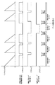
図19により最適タイマ値の再探索を説明する。最適タイマ値の再探索は、最適タイマ値省電力効果測定信号2563と省電力効果減少割込信号213を使用して実現される。図19の横軸は時間経過を示し、縦軸は機器状態、フレーム番号、各種信号の状態を示す。
The search for the optimum timer value will be described with reference to FIG. The search for the optimum timer value is realized by using the optimum timer value power saving
動画撮影処理(SD)において、動画撮影が開始される(T1)と、初期10フレームでタイマ値調整が行われ(T1-T2)、後続フレームで調整後の最適タイマ値「100」が使用される(T2-T3)。時刻T2でタイマ値調整が終了すると同時に、最適タイマ値省電力効果測定信号2563がアクティブになり、最適タイマ値「100」におけるフレームごとの省電力効果が継続して測定される。最適タイマ値省電力効果測定信号2563は、CPU10が設定レジスタ800の最適タイマ値省電力効果測定フィールドに‘1’をライトすることでアクティブになる。図19の例では、11フレーム目に省電力効果「570」、12フレーム目に省電力効果「550」が測定される。
In the movie shooting process (SD), when movie shooting is started (T1), the timer value is adjusted in the initial 10 frames (T1-T2), and the adjusted optimum timer value "100" is used in the subsequent frames. (T2-T3). At the same time as the timer value adjustment is completed at time T2, the optimum timer value power saving
図19の例では、タイマ値調整期間(T1-T2)における最適タイマ値「100」に対する省電力効果の値ETadjは「600」である。省電力効果測定・最適タイマ値判定モジュール2562は、タイマ値調整期間の省電力効果の値ETadjと、タイマ値調整期間終了後(T2-T3)のフレームごとの省電力効果の値ETを、タイマ値更新トリガ信号254の発生タイミングで比較する。比較の結果、下式が成立する場合、省電力効果測定・最適タイマ値判定モジュール2562は、省電力効果減少割込信号213をアサートする(T3)。
if (ET≦ETadj/2)
省電力効果減少割込信号213をアサート; …(3)
In the example of FIG. 19, the power saving effect value E Tadj for the optimum timer value “100” in the timer value adjustment period (T1-T2) is “600”. The power saving effect measurement / optimum timer
if (E T ≤ E Tadj / 2)
Assert power saving effect reduction interrupt
つまり、省電力効果減少割り込みの発生は、タイマ値調整期間(T1-T2)において決定した最適タイマ値によってフレーム処理を進めるに従い、省電力効果が減少したことを意味する。省電力効果減少割り込みを受信したCPU10は、再度タイマ値調整を実施する(T3-T4)。最適タイマ値の再探索におけるタイマ値の調整方法は最初のタイマ値調整(T1-T2)と同じ手順で実施される。
That is, the occurrence of the power saving effect reduction interrupt means that the power saving effect is reduced as the frame processing is advanced according to the optimum timer value determined in the timer value adjustment period (T1-T2). The
図19の例において、一回目のタイマ値調整と二回目のタイマ値調整のタイマ値調整用パラメータは同じ値で実施される。その結果、二回目のタイマ値調整(T3-T4)期間の最適タイマ値は「70」となり、二回目のタイマ値調整後(T4-T5)は最適タイマ値「70」を使用される。また、同時に、最適タイマ値「70」におけるフレームごとの省電力効果測定を継続され、再び式(3)が成立すると省電力効果減少割り込みが発生する。なお、一回目と二回目のタイマ値調整におけるタイマ値調整用パラメータは、同じ値に限らず、異なる値を設定しても構わない。 In the example of FIG. 19, the timer value adjustment parameters of the first timer value adjustment and the second timer value adjustment are executed with the same value. As a result, the optimum timer value during the second timer value adjustment (T3-T4) period becomes "70", and after the second timer value adjustment (T4-T5), the optimum timer value "70" is used. At the same time, the power saving effect measurement for each frame at the optimum timer value "70" is continued, and when the equation (3) is satisfied again, the power saving effect reduction interrupt occurs. The timer value adjustment parameters in the first and second timer value adjustments are not limited to the same value, and different values may be set.
上記では、動画撮影の動作モードを例に説明したが、アプリケーションや動作モードは限定されない。また、省電力効果の判定に、省電力モード期間と省電力モード移行期間をカウントして、その差分を用いる例を示したが、この判定方法は一例に過ぎず、例えば、省電力モード移行許可の総回数と省電力モード移行不許可の総回数の差分を用いてもよい。その場合、省電力モード移行成功回数測定部を用意して省電力モード移行許可の総回数をカウントし、省電力モード移行失敗回数測定部を用意して省電力モード移行不許可の総回数をカウントする。 In the above, the operation mode of moving image shooting has been described as an example, but the application and the operation mode are not limited. Further, an example is shown in which the power saving mode period and the power saving mode transition period are counted and the difference is used to judge the power saving effect. However, this judgment method is only an example, for example, the power saving mode transition permission is permitted. The difference between the total number of times of power saving mode transition and the total number of times of disallowing the transition to the power saving mode may be used. In that case, prepare a power saving mode transition success measurement unit to count the total number of power saving mode transition permission, and prepare a power saving mode transition failure measurement unit to count the total number of power saving mode transition disapproval. To do.
また、上記では、動画撮影を例に、各フレーム処理におけるインターバルタイマ251へのタイマ値入力に関し、タイマ値調整段階と調整後最適タイマ値採用段階に分けて制御する例を説明した。タイマ値調整段階では撮影している動画に最適なタイマ値は不明なため、予め決められたルールに基づきフレーム間でタイマ値を動的に変更し、調整タイマ値ごとの省電力効果を定量的に測定する。タイマ値調整段階の終了後、最も省電力効果が高かったタイマ値を最適タイマ値採用段階で使用する。これにより、最適タイマ値採用段階のバスモジュール100の非動作期間を適切に検出することができ、クロック停止期間を長くすることができ、その結果、省電力への寄与が期待される。
Further, in the above, an example of controlling the timer value input to the
[電力制御モジュールの他の構成]
以下、電力制御モジュール25の他の構成例を説明する。マスタモジュール300は、DMAC14、15などの周期的に多量のデータ転送を行うモジュール、および、キャッシュを内蔵するCPU10、11などの非周期的にキャッシュラインの入れ替えのための短いデータ転送を行うモジュールである。このような特性が異なるマスタモジュール300が混在して、バスシステム30に接続される。従って、バスシステム30には、特性が異なる転送データが混在する。
[Other configurations of power control module]
Hereinafter, other configuration examples of the
●属性生成回路
図4に示す属性生成回路106は、すべてのスレーブデータ転送制御I/F501が受信するデータ転送要求信号と、マスタIDを入力し、転送要求データ属性信号を生成する。属性生成回路106は、内部にCPUのID、DMACのIDを予め保持しており、入力したマスタIDから、データ転送要求信号を駆動したマスタモジュール300がCPUかDMACか識別可能である。データ転送要求信号がアクティブな全マスタがCPUであれば、転送要求データ属性信号をアクティブにする。データ転送要求信号がアクティブな全マスタがDMACであれば、転送要求データ属性信号をインアクティブにする。CPUとDMACが混在する場合、転送要求データ属性信号をインアクティブにする。
● Attribute generation circuit The
図20(a)のフローチャートにより属性生成回路106の動作を説明する。属性生成回路106は、データ転送要求信号が一つ以上アクティブの場合に動作を開始し、転送要求データ属性信号をインアクティブに初期化する(S401)。そして、データ転送要求信号[0]がアクティブか否かを判定する(S402)。データ転送要求信号[0]がアクティブと判定した場合は、対応するマスタID信号[0]がCPUのマスタIDと一致するか否かを判定する(S403)。マスタID信号[0]がCPUのマスタIDに一致すると判定した場合は、転送要求データ属性信号をアクティブにし(S404)、次のデータ転送要求信号[1]の判定処理(S402)を行う。
The operation of the
ステップS402でデータ転送要求信号[0]がアクティブではないと判定した場合、属性生成回路106は、ステップS403、S404をスキップして、次のデータ転送要求信号[1]の判定処理(S402)を行う。また、ステップS403でマスタID信号[0]がCPUのマスタIDと一致しない判定した場合、属性生成回路106は、転送要求データ属性信号をインアクティブにして(S405)、処理を終了する。
If it is determined in step S402 that the data transfer request signal [0] is not active, the
別の構成として、属性生成回路106がプロセッサが使用するプログラム領域のアドレス情報を備え、マスタID信号に代わりアドレス信号を入力する方法がある。データ転送要求がアクティブなアドレス信号がプログラム領域のアドレスか否かを判定し、アドレス信号がプログラム領域のアドレスの場合は転送要求データ属性信号をアクティブにする。
As another configuration, there is a method in which the
また、別の構成として、転送データに周期、非周期を示す属性信号を含め、データ転送要求信号を駆動するマスタモジュール300が転送データに応じて周期、非周期を切り替える。属性生成回路106は、マスタID信号に代わり属性信号を入力して、転送要求データ属性信号を制御する。
Further, as another configuration, the
●電力制御モジュール
図21(a)のブロック図により電力制御モジュール25の他の構成例を示す。電力制御モジュール25は、各バスモジュール100に対応する電力制御I/Fを有する。各電力制御I/Fは、省電力モードの移行と復帰を制御する制御モジュール250とインターバルタイマ251、インターバルタイマ251に設定する複数のリファレンス値252を有し、対応するバスモジュール100の状態を管理する。複数のリファレンス値252は異なる値であり、リファレンス値2はリファレンス値1に比較して充分に低い値とする。なお、各制御モジュール250は、電力制御モジュール25のCPUが電力制御モジュール25のROMなどに格納されたプログラムを実行することにより実現される。
● Power control module The block diagram in Fig. 21 (a) shows another configuration example of the
図20(b)のフローチャートにより複数のリファレンス値252を有する場合の制御モジュール250の処理を説明する。なお、図20(b)において、図8Aと同様の処理(S11-S20)の記載を省略する。
The processing of the
ステップS20の処理の後、制御モジュール250は、再び省電力モード移行要求を発行するか否かを判定し(S21)、省電力モード移行要求を発行しない場合は処理をステップS12に戻す。また、省電力モード移行要求を発行する場合は、転送要求データ属性信号がアクティブか否かを判定する(S41)。転送要求データ属性信号がアクティブではない場合、制御モジュール250は、インターバルタイマ251のカウント値countにリファレンス値1を設定する(S42)。また、転送要求データ属性信号がアクティブな場合、制御モジュール250は、インターバルタイマ251のカウント値countにリファレンス値2を設定し(S43)、処理をステップS13に戻す。
After the process of step S20, the
制御モジュール250による上記の処理により、CPU10、11などのマスタモジュール300による電力制御に関わる手続を軽減することが可能になる。さらに、バスモジュール100を省電力モードへ移行させた後、復帰トリガを受信するとき、復帰のトリガとなったデータ転送要求の転送要求データ属性に応じて、次に省電力モード移行要求信号をアクティブにするまでの期間を制御することが可能である。転送要求データ属性がアクティブのとき、つまり非周期的に発生するキャッシュラインの入れ替えのための短い転送要求データの場合は低い値であるリファレンス値2が選択される。また、転送要求データ属性がインアクティブの場合は高い値であるリファレンス値1が選択される。
The above processing by the
また、別の方法として、転送要求データ属性がアクティブの場合は低い値のリファレンス値2を設定するステップS43に遷移せずに、固定のサイクル後、省電力モード移行要求信号をアクティブにするステップS15に遷移してもよい。
Alternatively, if the transfer request data attribute is active, the power saving mode transition request signal is activated after a fixed cycle without transitioning to step S43 for setting a
●インターバルタイマのカウント値
図21(b)により電力制御信号とインターバルタイマ251のカウント値countの関係を説明する。
● Count value of interval timer Figure 21 (b) explains the relationship between the power control signal and the count value count of the
省電力モード移行要求信号がアクティブになった後、省電力モード応答信号がアクティブになるが省電力モード許可信号がアクティブにならない状況は、上述したように、バスモジュール100が省電力モードへの移行を許可しない場合である。この場合、電力制御モジュール25は、省電力モード移行要求信号が非アクティブにし、インターバルタイマ251に設定した時間が経過した後、再び省電力モード移行要求信号をアクティブにする。つまり、電力制御モジュール25は、CPU10や11の介在なしにインターバルタイマ251に設定した間隔で省電力モード移行要求を行う。
In the situation where the power saving mode response signal becomes active but the power saving mode permission signal does not become active after the power saving mode transition request signal becomes active, the
バスモジュール100は、データのロスやフリーズを避けるためのモード移行期間において、省電力モードへの移行が可能か否かを判定し、移行が可能であればその旨を電力制御モジュール25に通知する。電力制御モジュール25は、省電力モードへの移行が可能な状況においてのみ、電源やクロックを制御することができ、バスモジュール100の省電力化を行うことができる。
The
電力制御モジュール25は、複数のバスモジュール100に対応して複数のインターバルタイマ251を有する。各インターバルタイマ251の値は、転送要求データの特性に応じて切り替える。転送要求データがDMACの転送データのように周期的に転送する多量のデータの場合、電力制御モジュール25は、インターバルタイマ251に高い値のカウント値count1を設定して、省電力モード移行期間による実効性能の低下の機会を減らす。
The
また、CPUの転送データのように非周期的なキャッシュラインの入れ替えのための短いデータ転送の場合、電力制御モジュール25は、インターバルタイマ251に低い値のカウント値count2を設定して、速やかに省電力モードへ移行するよう制御する。つまり、転送要求データの特性を考慮して、転送の実効性能と電力消費の最適なバランスを得ることが可能になる。
Further, in the case of short data transfer for aperiodic cache line replacement such as CPU transfer data, the
以上の説明は、当業者が本発明を理解することができるように、本発明の原理、適用例を簡単に説明したものである。上記の説明に様々な変更が施した実施例が、特定の用途に適す場合があり得るが、それらは本発明の範囲に含まれる。例えば、図8A、図8B、図9においては、インターバルタイマ251がダウンカウンタの例を説明したが、インターバルタイマ251としてアップカウンタを利用することもできる。
The above description briefly describes the principle and application examples of the present invention so that those skilled in the art can understand the present invention. Examples with various modifications to the above description may be suitable for a particular application, but they are within the scope of the present invention. For example, in FIGS. 8A, 8B, and 9, the
このように、転送データのロスやフリーズを回避するためにマスタモジュール300に対する特別な処理を必要としない、電力制御が可能なバスシステム30を提供することができる。また、特別な専用回路を用いることなく、比較的簡単な仕組みで定期的に省電力モードに移行させることができるバスモジュール100を提供することができる。従って、電源遮断によるリーク電力の削減機会や、クロック遮断によるクロックツリーでのダイナミック電力の削減機会を増加させることができる。
In this way, it is possible to provide a
[その他の実施例]
本発明は、上述の実施形態の一以上の機能を実現するプログラムを、ネットワーク又は記憶媒体を介してシステム又は装置に供給し、そのシステム又は装置のコンピュータにおける一以上のプロセッサがプログラムを読み出し実行する処理でも実現可能である。また、一以上の機能を実現する回路(例えば、ASIC)によっても実現可能である。
[Other Examples]
The present invention supplies a program that realizes one or more functions of the above-described embodiment to a system or device via a network or storage medium, and one or more processors in the computer of the system or device reads and executes the program. It can also be realized by processing. It can also be realized by a circuit (for example, ASIC) that realizes one or more functions.
30 … バスシステム、300 … マスタモジュール、400 … スレーブモジュール、100 … バスモジュール100、25 … 電力制御モジュール、250 … 制御モジュール
30… Bus system, 300… Master module, 400… Slave module, 100…
Claims (15)
前記複数のバスモジュールそれぞれとの省電力モードへの移行の可否を示す通信及び機器状態に応じて調整された所定の時間が経過したか否かに基づき、各バスモジュールの省電力モードへの移行を制御する電力制御手段と、
を有し、
前記電力制御手段は、前記複数のバスモジュールそれぞれに対応し、対応するバスモジュールとの間で電力制御信号により前記通信を行う複数の制御手段を有する情報処理装置。 A data transfer means having a plurality of bus modules for transferring data between a plurality of master modules and at least one slave module,
Transition to the power saving mode of each bus module based on whether or not a predetermined time adjusted according to the communication and device status indicating whether or not the transition to the power saving mode with each of the plurality of bus modules has elapsed has elapsed. Power control means to control
Have,
The power control means is an information processing device having a plurality of control means corresponding to each of the plurality of bus modules and performing the communication with the corresponding bus modules by a power control signal.
各バスモジュールは、対応する制御手段から受信する前記要求信号がアクティブになると、前記データ転送受信準備信号を非アクティブにして転送データの非受信状態に移行し、処理中のデータ転送があるか否かの判定を行う請求項6に記載された情報処理装置。 Each of the plurality of bus modules transfers the data by a two-wire handshake using the data transfer request signal and the data transfer reception preparation signal.
When the request signal received from the corresponding control means becomes active, each bus module deactivates the data transfer reception preparation signal and shifts to the non-reception state of the transfer data, and whether or not there is data transfer being processed. The information processing apparatus according to claim 6, wherein the determination is made.
各制御手段は、対応するバスモジュールから受信中の前記許可信号が非アクティブに変化した場合に転送データの属性を受信し、前記転送データの属性に応じて、前記省電力モードを解除した後、再び、前記要求信号をアクティブにするまでの時間を制御する請求項6に記載された情報処理装置。 Further equipped with a power supply independent of the corresponding bus module and a data transfer detection module capable of setting the state of the permission signal regardless of whether the corresponding bus module is in power saving mode.
Each control means receives the attribute of the transfer data when the permission signal being received from the corresponding bus module changes inactively, and after canceling the power saving mode according to the attribute of the transfer data, The information processing apparatus according to claim 6, wherein the time until the request signal is activated is controlled again.
電力制御手段が、前記複数のバスモジュールそれぞれとの省電力モードへの移行の可否を示す通信及び機器状態に応じて調整された所定の時間が経過したか否かに基づき、各バスモジュールの省電力モードへの移行を制御し、
前記電力制御手段は、前記複数のバスモジュールそれぞれに対応する複数の制御手段を有し、各制御手段は、対応するバスモジュールとの間で電力制御信号により前記通信を行う制御方法。 A control method for a data transfer device having a plurality of bus modules that transfer data between a plurality of master modules and at least one slave module.
The power saving of each bus module is based on whether or not a predetermined time adjusted according to the communication and the device state indicating whether or not the power control means can shift to the power saving mode with each of the plurality of bus modules has elapsed. Control the transition to power mode,
A control method in which the power control means has a plurality of control means corresponding to each of the plurality of bus modules, and each control means communicates with the corresponding bus module by a power control signal.
Priority Applications (3)
| Application Number | Priority Date | Filing Date | Title |
|---|---|---|---|
| JP2014160802A JP6774160B2 (en) | 2013-12-06 | 2014-08-06 | Information processing device and data transfer device control method |
| US14/553,852 US9678562B2 (en) | 2013-12-06 | 2014-11-25 | Information processing apparatus, data transfer apparatus, and control method for data transfer apparatus |
| CN201410727879.XA CN104699642B (en) | 2013-12-06 | 2014-12-04 | The control method of information processor, data link and data link |
Applications Claiming Priority (3)
| Application Number | Priority Date | Filing Date | Title |
|---|---|---|---|
| JP2013253609 | 2013-12-06 | ||
| JP2013253609 | 2013-12-06 | ||
| JP2014160802A JP6774160B2 (en) | 2013-12-06 | 2014-08-06 | Information processing device and data transfer device control method |
Publications (3)
| Publication Number | Publication Date |
|---|---|
| JP2015130147A JP2015130147A (en) | 2015-07-16 |
| JP2015130147A5 JP2015130147A5 (en) | 2017-09-07 |
| JP6774160B2 true JP6774160B2 (en) | 2020-10-21 |
Family
ID=53271125
Family Applications (1)
| Application Number | Title | Priority Date | Filing Date |
|---|---|---|---|
| JP2014160802A Active JP6774160B2 (en) | 2013-12-06 | 2014-08-06 | Information processing device and data transfer device control method |
Country Status (3)
| Country | Link |
|---|---|
| US (1) | US9678562B2 (en) |
| JP (1) | JP6774160B2 (en) |
| CN (1) | CN104699642B (en) |
Families Citing this family (13)
| Publication number | Priority date | Publication date | Assignee | Title |
|---|---|---|---|---|
| CN104204975B (en) * | 2012-03-26 | 2016-10-12 | 三菱电机株式会社 | Sequencer debugging auxiliary device |
| KR102151178B1 (en) * | 2014-05-19 | 2020-09-02 | 삼성전자 주식회사 | Serial communication apparatus and method thereof |
| JP6425492B2 (en) * | 2014-10-17 | 2018-11-21 | キヤノン株式会社 | INFORMATION PROCESSING APPARATUS, INFORMATION PROCESSING METHOD, AND PROGRAM |
| US9690364B2 (en) * | 2015-09-04 | 2017-06-27 | Qualcomm Incorporated | Systems and methods for dynamically adjusting memory state transition timers |
| US9781679B2 (en) * | 2015-11-27 | 2017-10-03 | Samsung Electronics Co., Ltd. | Electronic systems and method of operating electronic systems |
| CN106126841B (en) * | 2016-06-30 | 2019-08-23 | 福州瑞芯微电子股份有限公司 | A kind of method and apparatus based on hardware frequency conversion |
| JP6977439B2 (en) * | 2017-09-20 | 2021-12-08 | ブラザー工業株式会社 | Electronics |
| JP6991812B2 (en) | 2017-09-26 | 2022-01-13 | キヤノン株式会社 | An information processing device equipped with a controller capable of communicating with a connected external device and shifting to a power saving state, and a control method thereof. |
| US11144457B2 (en) * | 2018-02-22 | 2021-10-12 | Netspeed Systems, Inc. | Enhanced page locality in network-on-chip (NoC) architectures |
| PT3688601T (en) | 2018-12-03 | 2020-11-13 | Hewlett Packard Development Co | Logic circuitry |
| CN110674063B (en) * | 2019-09-16 | 2021-03-23 | 上海天数智芯半导体有限公司 | Framework and method for realizing fabric in chip |
| JP2023009676A (en) * | 2021-07-07 | 2023-01-20 | キヤノン株式会社 | Arithmetic processing unit and control method thereof |
| US20230400333A1 (en) * | 2022-06-10 | 2023-12-14 | Badger Meter, Inc. | System and Method for Identifying the Effect of Changes in a Utility Monitoring System |
Family Cites Families (25)
| Publication number | Priority date | Publication date | Assignee | Title |
|---|---|---|---|---|
| US5504907A (en) * | 1991-02-14 | 1996-04-02 | Dell Usa, L.P. | Power management system with adaptive control parameters for portable computer |
| JPH08335357A (en) * | 1995-06-08 | 1996-12-17 | Fujitsu Ltd | Storage device |
| US6711691B1 (en) * | 1999-05-13 | 2004-03-23 | Apple Computer, Inc. | Power management for computer systems |
| US6631434B1 (en) * | 1999-11-15 | 2003-10-07 | Hewlett-Packard Development Company, L.P. | Dynamic early indication system for a computer |
| JP4733877B2 (en) | 2001-08-15 | 2011-07-27 | 富士通セミコンダクター株式会社 | Semiconductor device |
| US20030135676A1 (en) * | 2002-01-17 | 2003-07-17 | Koninklijke Philips Electronics N.V. | Low-power bus interface |
| US7155618B2 (en) * | 2002-03-08 | 2006-12-26 | Freescale Semiconductor, Inc. | Low power system and method for a data processing system |
| JP3654284B2 (en) * | 2002-10-03 | 2005-06-02 | 日本電気株式会社 | Wireless terminal apparatus and wireless communication system using the same |
| US7398403B2 (en) * | 2004-07-01 | 2008-07-08 | Matsushita Electric Industrial Co., Ltd. | Multiprocessor control apparatus, control method thereof, and integrated circuit |
| JP4455540B2 (en) | 2006-06-15 | 2010-04-21 | キヤノン株式会社 | Bus system and arbitration method |
| JP5023660B2 (en) * | 2006-10-31 | 2012-09-12 | コニカミノルタビジネステクノロジーズ株式会社 | Image forming apparatus and method for controlling image forming apparatus |
| JP4921283B2 (en) * | 2007-08-20 | 2012-04-25 | 株式会社日立製作所 | Semiconductor device |
| JP2009122922A (en) * | 2007-11-14 | 2009-06-04 | Panasonic Corp | Data processor |
| JP2010072897A (en) * | 2008-09-18 | 2010-04-02 | Nec Electronics Corp | Clock supply device |
| KR101375466B1 (en) * | 2009-01-12 | 2014-03-18 | 램버스 인코포레이티드 | Mesochronous signaling system with multiple power modes |
| US8448001B1 (en) * | 2009-03-02 | 2013-05-21 | Marvell International Ltd. | System having a first device and second device in which the main power management module is configured to selectively supply a power and clock signal to change the power state of each device independently of the other device |
| JP5725695B2 (en) * | 2009-03-16 | 2015-05-27 | キヤノン株式会社 | Data storage device and data storage device control method |
| US9286257B2 (en) * | 2011-01-28 | 2016-03-15 | Qualcomm Incorporated | Bus clock frequency scaling for a bus interconnect and related devices, systems, and methods |
| KR101842245B1 (en) * | 2011-07-25 | 2018-03-26 | 삼성전자주식회사 | Bus system in SoC and method of gating root clocks therefor |
| JP5775398B2 (en) * | 2011-08-25 | 2015-09-09 | ルネサスエレクトロニクス株式会社 | Semiconductor integrated circuit device |
| US20130117593A1 (en) * | 2011-11-07 | 2013-05-09 | Qualcomm Incorporated | Low Latency Clock Gating Scheme for Power Reduction in Bus Interconnects |
| JP2013106166A (en) * | 2011-11-14 | 2013-05-30 | Sony Corp | Clock gating circuit and bus system |
| CN104054037B (en) * | 2011-12-16 | 2016-10-12 | 日立麦克赛尔株式会社 | Reception equipment and power supply method |
| JP5146590B2 (en) * | 2011-12-20 | 2013-02-20 | コニカミノルタビジネステクノロジーズ株式会社 | Image forming apparatus and control method thereof |
| US9378132B2 (en) * | 2012-03-22 | 2016-06-28 | Hgst Technologies Santa Ana, Inc. | System and method for scanning flash memories |
-
2014
- 2014-08-06 JP JP2014160802A patent/JP6774160B2/en active Active
- 2014-11-25 US US14/553,852 patent/US9678562B2/en active Active
- 2014-12-04 CN CN201410727879.XA patent/CN104699642B/en active Active
Also Published As
| Publication number | Publication date |
|---|---|
| US20150160716A1 (en) | 2015-06-11 |
| US9678562B2 (en) | 2017-06-13 |
| CN104699642B (en) | 2018-04-24 |
| CN104699642A (en) | 2015-06-10 |
| JP2015130147A (en) | 2015-07-16 |
Similar Documents
| Publication | Publication Date | Title |
|---|---|---|
| JP6774160B2 (en) | Information processing device and data transfer device control method | |
| TWI533117B (en) | Apparatus,integrated circuit,and method for power management | |
| US9110671B2 (en) | Idle phase exit prediction | |
| TWI468926B (en) | Processor power management and method | |
| EP1286248B1 (en) | Semiconductor device with hardware mechanism for proper clock control | |
| US8127153B2 (en) | Memory power profiling | |
| TWI544323B (en) | Apparatus, computer-readable medium, method and system for increasing energy efficiency of sensor controllers | |
| US8806232B2 (en) | Systems and method for hardware dynamic cache power management via bridge and power manager | |
| TW201428760A (en) | Training, power-gating, and dynamic frequency changing of a memory controller | |
| JP2013025792A (en) | Flexible flash command | |
| TWI581092B (en) | Memory apparatus and energy-saving controlling method thereof | |
| US20140089546A1 (en) | Interrupt timestamping | |
| US20120133352A1 (en) | Voltage detection | |
| US10261927B2 (en) | DMA controller with trigger sequence generator | |
| JP2013025794A (en) | Effective utilization of flash interface | |
| JP2011095967A (en) | Bus sharing system | |
| JP6425492B2 (en) | INFORMATION PROCESSING APPARATUS, INFORMATION PROCESSING METHOD, AND PROGRAM | |
| JP5304815B2 (en) | Microcomputer | |
| US20060179172A1 (en) | Method and system for reducing power consumption of a direct memory access controller | |
| KR101564520B1 (en) | Information processing apparatus and scheduling method | |
| KR20230160854A (en) | Memory controller power states | |
| JP2014038502A (en) | Information processing device, information processing method, and program | |
| US9619386B2 (en) | Synchronization variable monitoring device, processor, and semiconductor apparatus | |
| US10552166B1 (en) | Data unit synchronization between chained pipelines | |
| JP4416575B2 (en) | Memory control method and memory control device |
Legal Events
| Date | Code | Title | Description |
|---|---|---|---|
| A521 | Request for written amendment filed |
Free format text: JAPANESE INTERMEDIATE CODE: A523 Effective date: 20170728 |
|
| A621 | Written request for application examination |
Free format text: JAPANESE INTERMEDIATE CODE: A621 Effective date: 20170728 |
|
| A977 | Report on retrieval |
Free format text: JAPANESE INTERMEDIATE CODE: A971007 Effective date: 20180725 |
|
| A131 | Notification of reasons for refusal |
Free format text: JAPANESE INTERMEDIATE CODE: A131 Effective date: 20180803 |
|
| A521 | Request for written amendment filed |
Free format text: JAPANESE INTERMEDIATE CODE: A523 Effective date: 20181002 |
|
| A02 | Decision of refusal |
Free format text: JAPANESE INTERMEDIATE CODE: A02 Effective date: 20190408 |
|
| A521 | Request for written amendment filed |
Free format text: JAPANESE INTERMEDIATE CODE: A523 Effective date: 20190708 |
|
| C60 | Trial request (containing other claim documents, opposition documents) |
Free format text: JAPANESE INTERMEDIATE CODE: C60 Effective date: 20190708 |
|
| A911 | Transfer to examiner for re-examination before appeal (zenchi) |
Free format text: JAPANESE INTERMEDIATE CODE: A911 Effective date: 20190716 |
|
| C21 | Notice of transfer of a case for reconsideration by examiners before appeal proceedings |
Free format text: JAPANESE INTERMEDIATE CODE: C21 Effective date: 20190719 |
|
| A912 | Re-examination (zenchi) completed and case transferred to appeal board |
Free format text: JAPANESE INTERMEDIATE CODE: A912 Effective date: 20190927 |
|
| C211 | Notice of termination of reconsideration by examiners before appeal proceedings |
Free format text: JAPANESE INTERMEDIATE CODE: C211 Effective date: 20191004 |
|
| C22 | Notice of designation (change) of administrative judge |
Free format text: JAPANESE INTERMEDIATE CODE: C22 Effective date: 20200403 |
|
| C22 | Notice of designation (change) of administrative judge |
Free format text: JAPANESE INTERMEDIATE CODE: C22 Effective date: 20200626 |
|
| C23 | Notice of termination of proceedings |
Free format text: JAPANESE INTERMEDIATE CODE: C23 Effective date: 20200720 |
|
| C03 | Trial/appeal decision taken |
Free format text: JAPANESE INTERMEDIATE CODE: C03 Effective date: 20200904 |
|
| C30A | Notification sent |
Free format text: JAPANESE INTERMEDIATE CODE: C3012 Effective date: 20200904 |
|
| A61 | First payment of annual fees (during grant procedure) |
Free format text: JAPANESE INTERMEDIATE CODE: A61 Effective date: 20201002 |
|
| R151 | Written notification of patent or utility model registration |
Ref document number: 6774160 Country of ref document: JP Free format text: JAPANESE INTERMEDIATE CODE: R151 |