JP6991812B2 - An information processing device equipped with a controller capable of communicating with a connected external device and shifting to a power saving state, and a control method thereof. - Google Patents
An information processing device equipped with a controller capable of communicating with a connected external device and shifting to a power saving state, and a control method thereof. Download PDFInfo
- Publication number
- JP6991812B2 JP6991812B2 JP2017185428A JP2017185428A JP6991812B2 JP 6991812 B2 JP6991812 B2 JP 6991812B2 JP 2017185428 A JP2017185428 A JP 2017185428A JP 2017185428 A JP2017185428 A JP 2017185428A JP 6991812 B2 JP6991812 B2 JP 6991812B2
- Authority
- JP
- Japan
- Prior art keywords
- usb
- controller
- usb controller
- external device
- information processing
- Prior art date
- Legal status (The legal status is an assumption and is not a legal conclusion. Google has not performed a legal analysis and makes no representation as to the accuracy of the status listed.)
- Active
Links
Images


Classifications
-
- H—ELECTRICITY
- H04—ELECTRIC COMMUNICATION TECHNIQUE
- H04N—PICTORIAL COMMUNICATION, e.g. TELEVISION
- H04N1/00—Scanning, transmission or reproduction of documents or the like, e.g. facsimile transmission; Details thereof
- H04N1/00885—Power supply means, e.g. arrangements for the control of power supply to the apparatus or components thereof
- H04N1/00888—Control thereof
-
- G—PHYSICS
- G06—COMPUTING OR CALCULATING; COUNTING
- G06F—ELECTRIC DIGITAL DATA PROCESSING
- G06F1/00—Details not covered by groups G06F3/00 - G06F13/00 and G06F21/00
- G06F1/26—Power supply means, e.g. regulation thereof
- G06F1/32—Means for saving power
- G06F1/3203—Power management, i.e. event-based initiation of a power-saving mode
- G06F1/3234—Power saving characterised by the action undertaken
- G06F1/3296—Power saving characterised by the action undertaken by lowering the supply or operating voltage
-
- G—PHYSICS
- G06—COMPUTING OR CALCULATING; COUNTING
- G06F—ELECTRIC DIGITAL DATA PROCESSING
- G06F1/00—Details not covered by groups G06F3/00 - G06F13/00 and G06F21/00
- G06F1/26—Power supply means, e.g. regulation thereof
- G06F1/266—Arrangements to supply power to external peripherals either directly from the computer or under computer control, e.g. supply of power through the communication port, computer controlled power-strips
-
- G—PHYSICS
- G06—COMPUTING OR CALCULATING; COUNTING
- G06F—ELECTRIC DIGITAL DATA PROCESSING
- G06F1/00—Details not covered by groups G06F3/00 - G06F13/00 and G06F21/00
- G06F1/26—Power supply means, e.g. regulation thereof
- G06F1/32—Means for saving power
- G06F1/3203—Power management, i.e. event-based initiation of a power-saving mode
- G06F1/3206—Monitoring of events, devices or parameters that trigger a change in power modality
- G06F1/3228—Monitoring task completion, e.g. by use of idle timers, stop commands or wait commands
-
- G—PHYSICS
- G06—COMPUTING OR CALCULATING; COUNTING
- G06F—ELECTRIC DIGITAL DATA PROCESSING
- G06F13/00—Interconnection of, or transfer of information or other signals between, memories, input/output devices or central processing units
- G06F13/38—Information transfer, e.g. on bus
- G06F13/42—Bus transfer protocol, e.g. handshake; Synchronisation
- G06F13/4282—Bus transfer protocol, e.g. handshake; Synchronisation on a serial bus, e.g. I2C bus, SPI bus
-
- H—ELECTRICITY
- H04—ELECTRIC COMMUNICATION TECHNIQUE
- H04N—PICTORIAL COMMUNICATION, e.g. TELEVISION
- H04N1/00—Scanning, transmission or reproduction of documents or the like, e.g. facsimile transmission; Details thereof
- H04N1/00885—Power supply means, e.g. arrangements for the control of power supply to the apparatus or components thereof
- H04N1/00907—Details of supply connection, e.g. arrangement of power cables
-
- G—PHYSICS
- G06—COMPUTING OR CALCULATING; COUNTING
- G06F—ELECTRIC DIGITAL DATA PROCESSING
- G06F2213/00—Indexing scheme relating to interconnection of, or transfer of information or other signals between, memories, input/output devices or central processing units
- G06F2213/0042—Universal serial bus [USB]
-
- Y—GENERAL TAGGING OF NEW TECHNOLOGICAL DEVELOPMENTS; GENERAL TAGGING OF CROSS-SECTIONAL TECHNOLOGIES SPANNING OVER SEVERAL SECTIONS OF THE IPC; TECHNICAL SUBJECTS COVERED BY FORMER USPC CROSS-REFERENCE ART COLLECTIONS [XRACs] AND DIGESTS
- Y02—TECHNOLOGIES OR APPLICATIONS FOR MITIGATION OR ADAPTATION AGAINST CLIMATE CHANGE
- Y02D—CLIMATE CHANGE MITIGATION TECHNOLOGIES IN INFORMATION AND COMMUNICATION TECHNOLOGIES [ICT], I.E. INFORMATION AND COMMUNICATION TECHNOLOGIES AIMING AT THE REDUCTION OF THEIR OWN ENERGY USE
- Y02D10/00—Energy efficient computing, e.g. low power processors, power management or thermal management
Landscapes
- Engineering & Computer Science (AREA)
- Theoretical Computer Science (AREA)
- General Engineering & Computer Science (AREA)
- Physics & Mathematics (AREA)
- General Physics & Mathematics (AREA)
- Computer Hardware Design (AREA)
- Multimedia (AREA)
- Signal Processing (AREA)
- Facsimiles In General (AREA)
- Accessory Devices And Overall Control Thereof (AREA)
- Power Sources (AREA)
- Information Transfer Systems (AREA)
Description
本発明は、接続された外部装置と通信可能であって省電力状態に移行が可能なコントローラを備える情報処理装置及びその制御方法に関する。 The present invention relates to an information processing device including a controller capable of communicating with a connected external device and capable of shifting to a power saving state, and a control method thereof.
近年のパソコンや複写機などの情報処理装置は、外部装置と通信を行うインターフェースを備えている。外部装置との通信を行うインターフェースとして、USB(Universal Serial Bus)やPCI express等のシリアルインターフェースが積極的に活用されている。プリンタやスキャナには、外部装置から送信されたプリントデータを受信したり、スキャンしたスキャンデータを外部装置に送信したりするために、USBコントローラを備えるものがある。 Information processing devices such as personal computers and copiers in recent years are equipped with an interface for communicating with an external device. As an interface for communicating with an external device, serial interfaces such as USB (Universal Serial Bus) and PCI express are actively utilized. Some printers and scanners are equipped with a USB controller in order to receive print data transmitted from an external device and to transmit scanned scan data to the external device.
上記したインターフェースの規格は、世の中のニーズに合わせて改訂が進められ、例えば、USB2.0の上位規格のUSB3.0のデータ転送速度(最大5Gbps)は、USB2.0のデータ転送速度(最大480Mbps)の約10倍となっている。また、USB3.0では、パワーマネジメント機能として、省電力効果別に、U1、U2、U3と呼ばれている低電力ステートが定義されている。 The above-mentioned interface standard is being revised according to the needs of the world. For example, the data transfer rate of USB3.0, which is a higher standard of USB2.0 (maximum 5 Gbps), is the data transfer rate of USB2.0 (maximum 480 Mbps). ) Is about 10 times. Further, in USB3.0, as a power management function, low power states called U1, U2, and U3 are defined for each power saving effect.
特許文献1に示されるように、USB3.0では、U1、U2、U3から外部装置と通信可能なU0に移行するときに、トレーニングシーケンスが実行される。このトレーニングシーケンスでは、例えば、TS1オーダードセットやTS2オーダードセットと呼ばれる周期性のあるパターンのデータを互いに送受信して、クロックデータリカバリ(CDR)を行う。このトレーニングシーケンスは、U1、U2、U3からU0に復帰するときに必ず実行される。さらに、U0からU1、U2、U3への移行は、USBバスがアイドル状態であることを条件に行われるため、プリント中やスキャン中であってもUSBバスがアイドル状態となれば、U0からU1、U2、U3への移行が実行される。そうすると、上記したような周期性のあるパターンのデータの送受信が、プリント中やスキャン中に頻繁に発生することによって、EMIのリスクが懸念される。
As shown in
そこで、本発明は、上記したような課題を解決するためになされたものである。その目的は、外部装置とデータの送受信を行うコントローラが低電力ステートから復帰するときに送受信される周期性のある所定パターンのデータによるEMIのリスクをソフトウェアによる制御で回避することである。 Therefore, the present invention has been made to solve the above-mentioned problems. The purpose is to avoid the risk of EMI due to a predetermined pattern of data transmitted and received periodically when the controller that transmits and receives data to and from the external device returns from the low power state by software control.
上記の課題を解決するため、本発明の情報処理装置は、USBバスを介して外部装置に画像データを送信し、所定の条件に基づいて低電力状態に移行可能なUSBコントローラであって、前記低電力状態からの復帰時に前記USBバスを介して所定パターンのデータを送信すると共に前記USBバスを介して所定パターンのデータを受信するUSBコントローラと、前記USBコントローラを用いるスキャンジョブを受付けたことに応じて、前記低電力状態への移行を禁止することを示す設定値を前記USBコントローラに対して設定し、当該スキャンジョブを実行することにより得られた画像データの前記USBバスを介した前記外部装置への送信を前記USBコントローラに行わせ、かつ、前記スキャンジョブが終了したことに応じて、前記USBコントローラに対して行われた前記設定値の設定を解除する制御手段と、を備える。 In order to solve the above problems, the information processing apparatus of the present invention is a USB controller capable of transmitting image data to an external device via a USB bus and shifting to a low power state based on a predetermined condition. A USB controller that transmits a predetermined pattern of data via the USB bus and receives a predetermined pattern of data via the USB bus when returning from a low power state, and a scan job using the USB controller are accepted. Accordingly, a setting value indicating that the transition to the low power state is prohibited is set for the USB controller, and the image data obtained by executing the scan job is the external via the USB bus. The USB controller is provided with a control means for causing the USB controller to perform transmission to the device and canceling the setting of the set value performed on the USB controller when the scan job is completed.
本発明によれば、外部装置とデータの送受信を行うインターフェースが低電力ステートから復帰するときに送受信される周期性のある所定パターンのデータによるEMIのリスクをソフトウェアによる制御で回避することができる。これにより、EMI対策のためのハードウェアの追加をすることなく(シールド部品の追加によるコストアップやシールド部品のための配置スペースの確保)、周期性のある所定パターンのデータによるEMIのリスクを回避することができる。 According to the present invention, it is possible to avoid the risk of EMI due to a predetermined pattern of data transmitted / received periodically when the interface for transmitting / receiving data to / from the external device returns from the low power state by software control. This avoids the risk of EMI due to periodic patterns of data without adding hardware for EMI countermeasures (increasing costs by adding shield parts and securing placement space for shield parts). can do.
[実施例1]
<画像形成装置>
図1は、実施例1の画像形成装置とPCとをUSBケーブルで接続したシステムを示している。
[Example 1]
<Image forming device>
FIG. 1 shows a system in which the image forming apparatus of the first embodiment and a PC are connected by a USB cable.
実施例1の画像形成装置100は、原稿の画像を読み取る読取部101、ユーザ操作を受け付ける操作部102、紙などの記録媒体に画像を印刷する記録部104、無線通信インターフェース(以下、無線通信IF)310、及び、FAX部317を備えている。また、画像形成装置100は、読取部101や記録部104等、画像形成装置100の全体の制御を行うコントローラ部103を備えている。画像形成装置100は、本発明の情報処理装置の一例である。
The
操作部102は、画像形成装置100のユーザから入力を受け付け、且つ、図示しない表示部に所定の画面を表示する。FAX部317は、公衆回線と通信可能に接続され、ファクシミリデータの送受信等を行う。無線通信IF310は、WifiやBluetooth(登録商標)等の無線通信で周辺機器とデータ通信を行う。
The
コントローラ部103は、USBコントローラ311を有している。このUSBコントローラ311とPC106とは、USBケーブル105を介して通信可能に接続されている。USBコントローラ311は、読取部101が読み取った原稿の画像のデータをPC106へ送信したり、PC106が送信した印刷データを受信したりする。
The
<コントローラ部>
コントローラ部103は、CPU304、ROM305、RAM306、HDD308を有する。CPU304は、ASIC307内に実装されている。CPU304は、ROM305内の初期プログラムに従って、メインプログラムをROM305から読み出し、RAM306に記憶する。RAM306は、プログラムの格納や、ワーク用のメインメモリとして使用される。HDD308は、プログラムや画像データ等を記録するために使用される。
<Controller part>
The
ASIC307には、上記したCPU304、USBコントローラ311、スキャナ通信インターフェース(以下、スキャナIF)312、プリンタ通信インターフェーフェース(以下、プリンタIF)313、が実装されている。また、ASIC307には、画像生成部309、色変換処理部318、及び、ハーフトーン処理部319が実装されている。
The ASIC 307 is equipped with the
画像生成部309は、PC106から受信した印刷データからラスターイメージデータを生成し、RGBデータを画素毎に出力する。また、画像生成部309は、読取部101によって読み取られた画像のデータを処理する。なお、読取部101は、少なくともCCD(Chaerged Couple Device)あるいはCIS(Contact Image Sensor)を含むものである。また、画像生成部309は、読み取った画像のデータに対して、所定の画像処理を行っても良い。
The
色変換処理部318は、画像生成部309によって生成されたRGBデータをトナー色であるCMYK変換する。CMYKデータは、CMYKのトナー量を示したデータになっており、画素単位に例えば0~255の8bitの値で表現される。具体的な値として、各色0であればトナー未使用を示し、値が大きくなるにつれて濃度は濃くなり、255で各色最大の濃さを意味する。
The color
ハーフトーン処理部319は、色変換処理部318から出力される各色のデータにハーフトーン処理を行う。ハーフトーン処理部319は、スクリーン処理や誤差拡散処理を行うによるものがある。スクリーン処理は、所定の複数のディザマトリクスおよび入力される画像データ用いて、N値化するものである。また、誤差拡散処理は、入力画像データの注目画素と所定の閾値と比較することにより、注目画素をN値化する処理を行い、N値化処理によって生じる注目画素と閾値との差分を、以降にN値化処理する周囲画素に対して拡散させる処理である。
The
プリンタIF313は、コントローラ部103と記録部104との間で通信を行うためのインターフェースである。ここで通信される情報としては、印刷する画像データのほか、コントローラ部103からの制御信号や、原稿タイプ設定や排紙設定等の情報が含まれる。プリント開始要求やプリントレディ通知など、コントローラ部103と記録部104との間で印刷動作シーケンスを同期して行う為の制御信号の送受信が行われる。
The printer IF 313 is an interface for communicating between the
スキャナIF312は、コントローラ部103と読取部101との間で通信を行うためのインターフェースである。ここで通信される情報としては、読取部101によって読み取られた原稿の画像データのほか、コントローラ部103から送信される制御信号が含まれる。
The scanner IF 312 is an interface for communicating between the
USBコントローラ311は、USB規格の定める仕様に基づいて動作するモジュールであって、外部のPC106とUSBケーブル105で接続されている。このUSBコントローラ311は、読取部101から出力された画像データを、USBケーブル105を介して、PC106へ送信することができる。また、USBコントローラ311は、PC106から出力された印刷データを、USBケーブル105を介して、記録部104へ送信することができる。次に、USBコントローラ311の詳細を説明する。
The
<USBコントローラ>
図2は、USBコントローラの詳細を示す図である。
<USB controller>
FIG. 2 is a diagram showing details of the USB controller.
USBコントローラ311は、SuperSpeed(高速)による通信制御を行うUSB3.1コントローラ(第1制御部)325、及び、USB3.1用のPHY327、を有する。また、USBコントローラ311は、HighSpeed/FullSpeed(低速)による通信制御を行うUSB2.0コントローラ(第2制御部)326、USB2.0用のPHY328、及び、バスパワーを検知するVBUS検知部329、を有する。
The
USB3.1コントローラ325は、USB2.0コントローラ326とは独立したコントローラであって、接続されるPC106との通信は、USB3.1コントローラ325及びUSB2.0コントローラ326の何れか一方が、排他的に行う。具体的には、VBUS検知部329が、Vbus供給部439からバスパワーが供給されていることを検知すると、PC106にSuperSpeedでの通信が可能なレシーバ(USB3.1コントローラ)が存在するか検知を行う。このレシーバの検知は、通信速度が速いコントローラから実施される。つまり、図2に示す構成であればSuperSpeedで通信可能なUSB3.1コントローラ325が、レシーバの検知を行う。一方、SuperSpeedで通信可能なレシーバが検知できない場合、USB2.0コントローラ326が、レシーバの検知を実施する。
The USB3.1
ここで、通信可能な状態とは、図3に示すLTSSMにおけるU0ステートである。LTSSM(Link Training Sequence State Machine)とは、USBインターフェースの状態と遷移条件を実装されたステートマシンである。 Here, the communicable state is the U0 state in the LTSSM shown in FIG. The LTSSM (Link Training Sequence Machine) is a state machine in which the state and transition conditions of the USB interface are implemented.
USBコントローラ311は、LTSSMに従って状態遷移を行うときに、PC106に所定のコマンドを送信することにより、PC106のUSBコントローラ411もUSBコントローラ311と同じ電力状態に移行する。
When the
また、USBコントローラ311は、タイマー331と、タイムアウトレジスタ332と、を有している。タイマー331は、USBバス(通信路)334がアイドル状態であればカウントし、カウント値がタイムアウトレジスタ332に設定された設定時間を超えると、PC106に低電力ステートへの移行要求コマンドを発行する。
Further, the
USB3.1コントローラ325は、CPU304によるアクセスが可能なLTSSMの状態遷移にかかわる制御レジスタ333を有する。この制御レジスタ333に、所定の値が入力されると(Application Specific Activity設定(以下、ASA設定)=0となると)、USBコントローラ311の電力状態は、U0ステートに固定される。つまり、ASA設定が「0」の間、USB3.1コントローラ325は、USBバス334がアイドル状態であっても、U1、U2、U3への移行を行わない。
The USB3.1
<LTSSM(Link Training Sequence State Machine)>
図3は、USB規格で定められるLTSSMの一部である。
<LTSSM (Link Training Sequence Machine)>
FIG. 3 is a part of LTSSM defined by the USB standard.
U0ステートは、通常の動作状態であり、PC106とのデータの送受信が可能な状態である。U1、U2、U3ステートは、低電力ステートであり、データの送受信ができない。また、低電力ステートから復帰するとき、まず、LFPS(Low Frequency Periodic Signaling)と呼ばれる方法でハンドシェイクを行なう。そして、Recoveryステートを経由して、トレーニングシーケンスを実行した後、U0ステートに遷移する。
The U0 state is a normal operating state, and is a state in which data can be transmitted / received to / from the
U0ステートから低電力ステート(U1、U2、U3ステート)への遷移は、接続されている相手装置とコマンドの送受信により行われる。図中のLGO_U1は、U1ステートへの移行要求を示すコマンドである。また、図中のLGO_U2は、U2ステートへの移行要求を示すコマンドであり、LGO_U3は、U3ステートへの移行要求を示すコマンドである。これらの移行要求コマンドは、USBバス334がアイドル状態で経過した時間が設定時間を超えることを条件に、相手装置に送信される。この設定時間は、CPU304が、タイムアウトレジスタ332に設定する。
The transition from the U0 state to the low power state (U1, U2, U3 state) is performed by sending and receiving a command to and from the connected remote device. LGO_U1 in the figure is a command indicating a transition request to the U1 state. Further, LGO_U2 in the figure is a command indicating a transition request to the U2 state, and LGO_U3 is a command indicating a transition request to the U3 state. These migration request commands are transmitted to the remote device on condition that the time elapsed in the idle state of the
<低電力ステートへの移行シーケンス>
図4は、低電力ステートへの移行シーケンスを示す図である。図中のLGO_U1は、U1ステートへの移行要求コマンド、LAUは、移行要求コマンドに対する移行許可コマンド、LPMAは移行許可コマンドを受理したことを示す受理コマンド、LXUは移行要求を拒否する移行拒否コマンドである。
<Transition to low power state>
FIG. 4 is a diagram showing a transition sequence to the low power state. In the figure, LGO_U1 is a migration request command to the U1 state, LAU is a migration permission command for the migration request command, LPMA is an acceptance command indicating that the migration permission command has been accepted, and LXU is a migration refusal command that rejects the migration request. be.
図4(A)は、U1ステートへの遷移が許可されるケースのシーケンスを示している。PC106のUSBコントローラ411がU1ステートへの移行条件を満たしたと判断すると、USBコントローラ411は、USBコントローラ311に、移行要求コマンドLGO_U1を送信する。画像形成装置100は、LGO_U1に対する応答として、移行許可コマンドLAUを返信する。そして、PC106のUSBコントローラ411は、LAUを受理したことを示す受理コマンドLPMAを、USBコントローラ311に送信する。これらのコマンドの送受信を行った上で、USBコントローラ311及びUSBコントローラ411が共にU1ステートへ移行する。
FIG. 4A shows a sequence of cases in which the transition to the U1 state is permitted. When it is determined that the
一方、図4(B)は、U1ステートへの遷移が拒否されるケースのシーケンスを示している。PC106のUSBコントローラ411がU1ステートへの移行条件を満たしたと判断すると、USBコントローラ311に、移行要求コマンドLGO_U1を送信する。USBコントローラ311は、LGO_U1に対して、移行拒否コマンドLXUを返信する。例えば、USBコントローラ311のASA設定が「0」であれば、USBコントローラ311は、移行拒否コマンドLXUを送信して、低電力ステートへの移行を拒否する。
On the other hand, FIG. 4B shows a sequence of cases in which the transition to the U1 state is rejected. When it is determined that the
<低電力ステートへの移行シーケンス>
図5は、USBコントローラが低電力ステートに移行するとき動作を示すフローチャートである。このフローチャートは、USBコントローラ311のUSB3.1コントローラ(電力制御手段)325が実行する。USBコントローラ311は、まず、ASA設定を確認する(S601)。ASA設定が「1」である場合(S601:No)、USB3.1コントローラ325は、PC106からLGO_U1を受信したか否かを判断する(S602)。LGO_U1を受信すると(S602:Yes)、USB3.1コントローラ325は、LXUをPC106に送信する(S603)。
<Transition to low power state>
FIG. 5 is a flowchart showing the operation when the USB controller shifts to the low power state. This flowchart is executed by the USB 3.1 controller (power control means) 325 of the
ステップS601において、ASA設定が「1」である場合(S601:Yes)、タイマー331のカウント値が、タイムアウトレジスタ332に設定された時間を超えたか否かを判断する(S604)。タイマー331のカウント値が、タイムアウトレジスタ332に設定された時間を超えた場合(S604:Yes)、USB3.1コントローラ325は、LGO_U1を送信する(S609)。次に、PC106からLAUを受信すると(S610:Yes)、PC106へLPMAを送信する(S611)。そして、USB3.1コントローラ325は、U1ステートへ遷移する(S608)。
In step S601, when the ASA setting is "1" (S601: Yes), it is determined whether or not the count value of the
S604において、タイマー331のカウント値が、タイムアウトレジスタ332に設定された時間を超えていない場合(S604:No)、USB3.1コントローラ325は、PC106からLGO_U1を受信したかどうかを判断する(S605)。そして、LGO_U1受信した場合、USB3.1コントローラ325は、PC106へLAUを送信する(S606)。次に、USB3.1コントローラ325は、PC106からLPMAを受信すると(S607:Yes)、U1ステートへ遷移する(S608)。
In S604, when the count value of the
図示の例では、U1ステートへの移行要求に対する動作フローを示したが、U2ステート及びU3ステートへの遷移も同様である。 In the illustrated example, the operation flow for the transition request to the U1 state is shown, but the transition to the U2 state and the U3 state is also the same.
<低電力ステートからの復帰シーケンス>
図6は、USBコントローラが低電力ステートから復帰するときに実行されるトレーニングのシーケンスを示した図である。図6の「Link State」は、USBコントローラの状態を示す。また、「LinkPartner1」は、画像形成装置100からPC106へ送信される信号を示し、「LinkPartner2」は、PC106から画像形成装置100への送信される信号を示している。
<Return sequence from low power state>
FIG. 6 shows a sequence of training performed when the USB controller returns from the low power state. “Link State” in FIG. 6 indicates the state of the USB controller. Further, "LinkPartner1" indicates a signal transmitted from the
まず、USBコントローラの状態は、低電力ステート(U1、U2、U3のいずれか)となっている。時刻「t10」において、復帰イベントが発生する。復帰イベントとは、画像形成装置100からPC106へのデータの送信などが挙げられる。時刻「t10」において、画像形成装置100のUSB3.1コントローラ325は、LFPS(Low Frequency Periodic Signaling)信号を、PC106に送信する。このLFPS信号とは、USB規格で定められた信号であって、復帰時の高速通信を始める前の初期通信において使われる低周波バースト信号である。
First, the state of the USB controller is a low power state (any of U1, U2, and U3). A return event occurs at time "t10". Examples of the return event include transmission of data from the
画像形成装置100からのLFPS信号を受信したPC106は、時刻「t11」において、画像形成装置100にLFPS信号を送信する。次に、時刻「t12」において、画像形成装置は、PC106から送信されたLFPS信号の受信後に、Recoveryステートへ遷移する。時刻「t10」から「t12」までの期間は、LFPS handshakeステートであり、その後に、Recoveryステートとなる。
Upon receiving the LFPS signal from the
Recoveryステートになると、USBコントローラ311は、U0ステートへの復帰に向けて、図8に示すTS1と呼ばれる信号(以下、TS1信号)を送信する。また、PC106も、画像形成装置100と同様に、LFPS信号を一定時間出力した後に、時刻「t13」でTS1信号を送信する。TS1信号は、USB規格で定められたものであり、その目的は、安定して通信が行える状態であることを確認することであり、具体的には、クロックデータリカバリが正常に行えることを確認している。
In the Recovery state, the
<TS1オーダードセット>
図7は、USB規格の定めるTS1オーダードセットを示している。役割としては、先に示したトレーニングシーケンスにおけるクロックデータリカバリが正常に行えるかを確認する目的で実施される。TS1オーダードセットは、構成するデータの定義中のSymbol Number「6-15」にTS1識別子としてD10.2符号が規定されている。
<TS1 ordered set>
FIG. 7 shows a TS1 ordered set defined by the USB standard. Its role is to confirm whether the clock data recovery in the training sequence shown above can be performed normally. In the TS1 ordered set, the Symbol Number "6-15" in the definition of the constituent data defines the D10.2 code as the TS1 identifier.
<D10.2符号>
図8は、8B10Bのコード表の一部である。8B10Bは、シリアルインターフェースに用いられる符号化方式であって、8ビットのデータを10ビットのシンボルに変換して伝送する符号化方式である。図7に示すTS1オーダードセットに規定のあるD10.2の符号化ビット列を示す。図示の「Data Byte Name」のD10.2は、符号名であり、「Data Byte Value」の4Aは、D10.2を示す値(16進法)である。また、Bits HGF EDCBA(binary)は、符号化の入力ビットに対応するデータを2進表記したものである。また、「Current RD-abcdiefghj」及び「Current RD+abcdiefghj」は、符号化の出力データパターンのbit列を示している。このように、bit列が‘0’及び‘1’が繰り返すデータであることが分かる。このように周期性のある所定パターンのデータを送受信すると、EMIの発生要因になる可能性がある。
<D10.2 code>
FIG. 8 is a part of the 8B10B code table. 8B10B is a coding method used for a serial interface, which is a coding method for converting 8-bit data into a 10-bit symbol and transmitting the data. The coded bit string of D10.2 specified in the TS1 ordered set shown in FIG. 7 is shown. D10.2 of the illustrated "Data Byte Name" is a code name, and 4A of "Data Byte Value" is a value (hexadecimal system) indicating D10.2. Further, Bits HGF ED CBA (binary) is a binary notation of data corresponding to an input bit of coding. Further, "Current RD-abcddiefghj" and "Current RD + abcdiefghj" indicate a bit string of a coded output data pattern. In this way, it can be seen that the bit column is the data in which "0" and "1" are repeated. Sending and receiving data of a predetermined pattern having periodicity in this way may cause EMI.
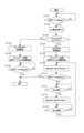
<フローチャート>
図9は、ASA設定を行う動作を示すフローチャートである。このフローチャートは、CPU304が実行する。
<Flow chart>
FIG. 9 is a flowchart showing the operation of setting the ASA. This flowchart is executed by the
実施例1の画像形成装置100のCPU304は、USBポート330にUSBケーブルが接続されたか否かを判断する(S1001)。接続相手のレシーバ検知動作に基づいて、接続するコントローラを選択し、且つ、リンク速度の判断が行われる(S1002)。CPU304は、SuperSpeedでリンクするか否かを判断し(S1003)、SuperSpeedでリンクすると判断した場合(S1003:Yes)、USB3.1コントローラ325及びPHY327の初期設定を行う(S1008)。SuperSpeedでリンクしないと判断した場合(S1003:Yes)、USB2.0コントローラ326および2.0PHY328の初期設定を行う(S1004)。
The
ステップS1004の後、CPU304は、エニュメレート処理を実行する(S1005)。エニュメレート処理では、PC106とUSB2.0コントローラ326とが、所定のデータのやり取りを行う。具体的には、USB2.0コントローラ326は、ディスクリプターと呼ばれるデバイス情報(通信相手先のアドレス情報、装置の属性、装置の設定情報)を保持しており、PC106にディスクリプターを送信する。PC106は、USB2.0コントローラ326から送信されたディスクリプタデータを解析して、USBコントローラの構成を理解する。そして、CPU304は、USBケーブルがプラグアウトされるまで、ジョブの実行指示の受け付けと、ジョブの実行とを行う(S1006)。
After step S1004, the
ステップS1008の後、USB3.1コントローラ325は、SpuerSpeedで通信接続を開始するためのエニュメレート処理を実施する(S1009)。このエニュメレート処理は、上記したエニュメレート処理と同様であるので、その説明を割愛する。ここで、実施例1では、CPU304は、制御レジスタ333を制御して、省電力ステートへの遷移許可設定(ASA設定=1)を行う(S1010)。
After step S1008, the USB3.1
次に、CPU304は、USBコントローラ311を使用するジョブを受け付けたかどうかを判断する(S1011)。USBコントローラ311を使用するジョブとは、PC106からのプリント指示に基づくプリントジョブ、あるいは、画像形成装置100の読取部101によって読み取られた画像のデータをPC106に送信するスキャンジョブを少なくとも含む。
Next, the
ステップS1011において、USBコントローラ311を使用するジョブを受け付けたと判断した場合、CPU304は、制御レジスタ333を制御して、省電力ステートへの遷移拒否設定(ASA設定=0)を行う(S1012)。そして、遷移拒否設定後に、ジョブを実行する(S1013)。これにより、ジョブの実行が完了するまでの間に、PC106と画像形成装置100との間でデータ(スキャンデータ、プリントデータ)の送信が行われる。そして、CPU304は、ジョブが終了をしたかどうかを判断し(S1014)、ジョブが終了したと判断した場合は、省電力ステートへの遷移許可設定(ASA設定=1)を行う(S1012)。
When it is determined in step S1011 that the job using the
次に、USBケーブルがプラグアウトされたか否かを判断し(S1016)、USBケーブルがプラグアウトされれば、このフローチャートを終了する。 Next, it is determined whether or not the USB cable has been plugged out (S1016), and if the USB cable is plugged out, this flowchart ends.
このように、実施例1では、ジョブを受け付けたことに基づいて、省電力ステートへの遷移設定(ASA設定=0)を行う。これにより、画像形成装置100とPC106との間で、ジョブの実行に伴うデータの送信中にUSB3.1コントローラ325が低電力ステートに移行するのを禁止することができる。よって、USB3.1コントローラ325は、データの送信中にトレーニングシーケンスを実行しない(TS1信号が出力されない)ので、トレーニングシーケンスに伴うEMIが発生しない。
As described above, in the first embodiment, the transition setting to the power saving state (ASA setting = 0) is performed based on the acceptance of the job. Thereby, it is possible to prohibit the USB3.1
[実施例2]
実施例1では、ジョブを受け付けたことに基づいて、省電力ステートへの遷移拒否設定(ASA設定=0)を行った。実施例2では、画像形成装置100がスタンバイモードになったことに基づいて、省電力ステートへの遷移拒否設定(ASA設定=0)を行う。
[Example 2]
In the first embodiment, the transition refusal setting (ASA setting = 0) to the power saving state is performed based on the acceptance of the job. In the second embodiment, the transition refusal setting (ASA setting = 0) to the power saving state is performed based on the fact that the
図10は、実施例2の画像形成装置のCPUがASA設定する動作を示すフローチャートである。 FIG. 10 is a flowchart showing an operation in which the CPU of the image forming apparatus of the second embodiment sets ASA.
実施例2の画像形成装置100は、スタンバイモードと、スタンバイモードよりも消費電力が少ないスリープモードと、を有している。実施例2の画像形成装置の構成は、実施例1の画像形成装置と同様であるので、その説明は割愛する。実施例2の画像形成装置は、スタンバイモードのときにユーザからの入力や外部装置からのデータの入力が所定時間なければ、スリープモードへ移行する。また、図示しない節電ボタンがユーザによって押下されたときにも、スタンバイモードからスリープモードに移行する。
The
実施例2では、スタンバイモードでは、省電力ステートへの遷移拒否設定(ASA設定=0)を行い、スリープモードでは、省電力ステートへの遷移許可設定(ASA設定=1)を行う。 In the second embodiment, the transition refusal setting to the power saving state (ASA setting = 0) is set in the standby mode, and the transition permission setting to the power saving state (ASA setting = 1) is set in the sleep mode.
S1101からS1108の各ステップは、実施例1と同様であるので、その説明を割愛する。エニュメレート処理が実行されると、CPU304は、省電力ステートへの遷移設定を、拒否設定(ASA設定=0)にする(S1109)。その後、画像形成装置100がスリープモードへの移行条件を満たすと(S1111)、CPU304は、遷移設定を、許可設定(ASA設定=1)にする(S1112)。また、画像形成装置100がスタンバイモードへの復帰条件を満たすと(S1113)、遷移設定を、拒否設定(ASA設定=0)にする(S1109)。
Since each step of S1101 to S1108 is the same as that of the first embodiment, the description thereof will be omitted. When the enumeration process is executed, the
実施例2の画像形成装置100では、スタンバイモード中にジョブが実行される。したがって、実施例2のように、スタンバイモード中に省電力ステートへの遷移拒否設定にしておくことによって、スタンバイモード中にトレーニングシーケンスが実行されることがない。よって、USBコントローラ311は、スタンバイモード中にトレーニングシーケンスを実行しない(TS1信号が出力されない)ので、トレーニングシーケンスに伴うEMIが発生しない。
In the
(その他の実施例)
上記した実施例では、画像形成装置に本発明を適用する例について説明したが、本発明をパソコンなどの情報処理装置に適用しても構わない。
(Other examples)
In the above-described embodiment, an example in which the present invention is applied to an image forming apparatus has been described, but the present invention may be applied to an information processing apparatus such as a personal computer.
また、本発明のコントローラは、USB規格のコントローラだけでなく、PCI規格のコントローラ、IEEE1394規格のコントローラ、などシリアル通信の規格のコントローラであってもよい。 Further, the controller of the present invention may be not only a USB standard controller but also a serial communication standard controller such as a PCI standard controller or an IEEE1394 standard controller.
また、本発明の目的は、前述した実施形態の機能を実現するソフトウェアのプログラムコードを記録した記録媒体を、システムあるいは装置に供給するよう構成することによっても達成される。この場合、そのシステムあるいは装置のコンピュータ(またはCPUやMPU)が記録媒体に格納されたプログラムコードを読出し実行することにより、上記機能が実現されることとなる。なお、この場合、そのプログラムコードを記憶した記録媒体は本発明を構成することになる。 An object of the present invention is also achieved by configuring a recording medium on which a program code of software that realizes the functions of the above-described embodiment is recorded to be supplied to a system or an apparatus. In this case, the above function is realized by the computer (or CPU or MPU) of the system or the device reading and executing the program code stored in the recording medium. In this case, the recording medium in which the program code is stored constitutes the present invention.
プログラムコードを供給するための記録媒体としては、例えば、フレキシブルディスク、ハードディスク、光ディスク、光磁気ディスク、CD-ROM、CD-R、磁気テープ、不揮発性のメモリカード、ROMなどを用いることができる。 As the recording medium for supplying the program code, for example, a flexible disk, a hard disk, an optical disk, a magneto-optical disk, a CD-ROM, a CD-R, a magnetic tape, a non-volatile memory card, a ROM, or the like can be used.
また、コンピュータが読出したプログラムコードを実行することにより、前述した実施形態の機能が実現される場合に限られない。例えば、そのプログラムコードの指示に基づき、コンピュータ上で稼働しているOS(オペレーティングシステム)などが実際の処理の一部または全部を行い、その処理によって前述した実施形態の機能が実現される場合も含まれる。 Further, the present invention is not limited to the case where the function of the above-described embodiment is realized by executing the program code read by the computer. For example, an OS (operating system) running on a computer may perform a part or all of the actual processing based on the instruction of the program code, and the processing may realize the function of the above-described embodiment. included.
さらに、記録媒体から読出されたプログラムコードが、コンピュータに挿入された機能拡張ボードやコンピュータに接続された機能拡張ユニットに備わるメモリに書込まれた後、前述した実施形態の機能が実現される場合も含まれる。つまり、プログラムコードがメモリに書込まれた後、そのプログラムコードの指示に基づき、その機能拡張ボードや機能拡張ユニットに備わるCPUなどが実際の処理の一部または全部を行い、その処理によって実現される場合も含まれる。 Further, when the function of the above-described embodiment is realized after the program code read from the recording medium is written in the memory provided in the function expansion board inserted in the computer or the function expansion unit connected to the computer. Is also included. That is, after the program code is written in the memory, the CPU provided in the function expansion board or the function expansion unit performs a part or all of the actual processing based on the instruction of the program code, and is realized by the processing. Is also included.
100 画像形成装置
311 USBコントローラ
325 USB3.1コントローラ
327 PHY
333 制御レジスタ
100
333 control register
Claims (8)
前記USBコントローラを用いるスキャンジョブを受付けたことに応じて、前記低電力状態への移行を禁止することを示す設定値を前記USBコントローラに対して設定し、
当該スキャンジョブを実行することにより得られた画像データの前記USBバスを介した前記外部装置への送信を前記USBコントローラに行わせ、かつ、
前記スキャンジョブが終了したことに応じて、前記USBコントローラに対して行われた前記設定値の設定を解除する制御手段と、を備えることを特徴とする情報処理装置。 A USB controller capable of transmitting image data to an external device via a USB bus and shifting to a low power state based on a predetermined condition, and having a predetermined pattern via the USB bus when returning from the low power state. A USB controller that transmits data and receives a predetermined pattern of data via the USB bus.
In response to the acceptance of the scan job using the USB controller, a setting value indicating that the transition to the low power state is prohibited is set for the USB controller.
The USB controller is made to transmit the image data obtained by executing the scan job to the external device via the USB bus, and
An information processing apparatus comprising: a control means for canceling the setting of the set value performed on the USB controller in response to the completion of the scan job.
前記USBデバイスコントローラは、前記低電力状態への移行が禁止されているとき、前記移行要求への応答として前記移行拒絶を送信する、ことを特徴とする請求項2に記載の情報処理装置。 The USB device controller can receive a migration request from the external device for requesting a transition to the low power state, and the migration permission or migration to the external device is possible in response to the migration request. It is possible to send any of the rejections,
The information processing apparatus according to claim 2, wherein the USB device controller transmits the transition refusal as a response to the transition request when the transition to the low power state is prohibited.
前記USBコントローラを用いるスキャンジョブを受付けたことに応じて、前記低電力状態への移行を禁止することを示す設定値を前記USBコントローラに対して設定するステップと、
当該スキャンジョブを実行することにより得られた画像データの前記USBバスを介した前記外部装置への送信を前記USBコントローラに行わせるステップと、
前記スキャンジョブが終了したことに応じて、前記USBコントローラに対して行われた前記設定値の設定を解除する解除ステップとを有することを特徴とする情報処理装置の制御方法。 A USB controller capable of transmitting image data to an external device via a USB bus and shifting to a low power state based on a predetermined condition, and having a predetermined pattern via the USB bus when returning from the low power state. It is a control method of an information processing apparatus that controls a USB controller that transmits data and receives data of a predetermined pattern via the USB bus.
A step of setting a setting value indicating that the transition to the low power state is prohibited for the USB controller according to the acceptance of the scan job using the USB controller, and
A step of causing the USB controller to transmit image data obtained by executing the scan job to the external device via the USB bus.
A method for controlling an information processing apparatus, which comprises a release step for canceling the setting of the set value performed on the USB controller in response to the completion of the scan job.
Priority Applications (3)
| Application Number | Priority Date | Filing Date | Title |
|---|---|---|---|
| JP2017185428A JP6991812B2 (en) | 2017-09-26 | 2017-09-26 | An information processing device equipped with a controller capable of communicating with a connected external device and shifting to a power saving state, and a control method thereof. |
| US16/128,320 US11500450B2 (en) | 2017-09-26 | 2018-09-11 | Information processing apparatus including controller capable of communicating with connected external apparatus and shifting to power-saving state, and control method therefor |
| CN201811125154.8A CN109561233B (en) | 2017-09-26 | 2018-09-26 | Information processing apparatus, control method therefor, and storage medium |
Applications Claiming Priority (1)
| Application Number | Priority Date | Filing Date | Title |
|---|---|---|---|
| JP2017185428A JP6991812B2 (en) | 2017-09-26 | 2017-09-26 | An information processing device equipped with a controller capable of communicating with a connected external device and shifting to a power saving state, and a control method thereof. |
Publications (3)
| Publication Number | Publication Date |
|---|---|
| JP2019062393A JP2019062393A (en) | 2019-04-18 |
| JP2019062393A5 JP2019062393A5 (en) | 2020-11-12 |
| JP6991812B2 true JP6991812B2 (en) | 2022-01-13 |
Family
ID=65806650
Family Applications (1)
| Application Number | Title | Priority Date | Filing Date |
|---|---|---|---|
| JP2017185428A Active JP6991812B2 (en) | 2017-09-26 | 2017-09-26 | An information processing device equipped with a controller capable of communicating with a connected external device and shifting to a power saving state, and a control method thereof. |
Country Status (3)
| Country | Link |
|---|---|
| US (1) | US11500450B2 (en) |
| JP (1) | JP6991812B2 (en) |
| CN (1) | CN109561233B (en) |
Citations (6)
| Publication number | Priority date | Publication date | Assignee | Title |
|---|---|---|---|---|
| JP2012132961A (en) | 2010-12-20 | 2012-07-12 | Konica Minolta Business Technologies Inc | Image forming apparatus |
| JP2012218248A (en) | 2011-04-06 | 2012-11-12 | Canon Inc | Image forming apparatus, and control method of the same |
| JP2013090006A (en) | 2011-10-13 | 2013-05-13 | Nikon Corp | Electronic apparatus and program |
| JP2016213703A (en) | 2015-05-11 | 2016-12-15 | キヤノン株式会社 | Image forming apparatus, control method therefor, and program |
| JP2016221947A (en) | 2015-05-28 | 2016-12-28 | キヤノン株式会社 | Image forming apparatus, control method therefor, and program |
| JP2017140708A (en) | 2016-02-08 | 2017-08-17 | キヤノン株式会社 | Communication control method, program and printing device |
Family Cites Families (12)
| Publication number | Priority date | Publication date | Assignee | Title |
|---|---|---|---|---|
| JP5029823B2 (en) | 2007-09-06 | 2012-09-19 | コニカミノルタビジネステクノロジーズ株式会社 | Image forming apparatus, power consumption management system, power consumption management method, and program |
| US8332676B2 (en) * | 2009-09-24 | 2012-12-11 | Intel Mobile Communications GmbH | Methods of preparing a power saving state, universal serial bus device and universal serial bus host |
| JP5426326B2 (en) | 2009-11-09 | 2014-02-26 | ルネサスエレクトロニクス株式会社 | Data receiving apparatus, data receiving method, and program |
| CN102081581B (en) | 2010-10-01 | 2013-10-30 | 威盛电子股份有限公司 | Power management system and method |
| CN102354305B (en) | 2011-09-27 | 2016-08-03 | 青岛海信电器股份有限公司 | Serial communication system between devices and method |
| US9338320B2 (en) * | 2012-08-10 | 2016-05-10 | Konica Minolta, Inc. | Image forming apparatus and method of controlling the same |
| JP6774160B2 (en) | 2013-12-06 | 2020-10-21 | キヤノン株式会社 | Information processing device and data transfer device control method |
| US9696777B2 (en) | 2014-06-05 | 2017-07-04 | Lenovo (Singapore) Pte. Ltd. | Computer port control |
| JP6397234B2 (en) | 2014-06-19 | 2018-09-26 | キヤノン株式会社 | Image forming apparatus, image forming apparatus control method, and program |
| JP2016045706A (en) * | 2014-08-22 | 2016-04-04 | ルネサスエレクトロニクス株式会社 | Information processing device, peripheral device control method, and filter driver |
| JP6415253B2 (en) * | 2014-11-10 | 2018-10-31 | キヤノン株式会社 | Image forming system, control method of image forming apparatus in the system, and program |
| TWM501592U (en) * | 2015-01-30 | 2015-05-21 | Asix Electronics Corp | Universal serial bus (USB) KVM switch using virtual USB for switching among multiple hosts |
-
2017
- 2017-09-26 JP JP2017185428A patent/JP6991812B2/en active Active
-
2018
- 2018-09-11 US US16/128,320 patent/US11500450B2/en active Active
- 2018-09-26 CN CN201811125154.8A patent/CN109561233B/en active Active
Patent Citations (6)
| Publication number | Priority date | Publication date | Assignee | Title |
|---|---|---|---|---|
| JP2012132961A (en) | 2010-12-20 | 2012-07-12 | Konica Minolta Business Technologies Inc | Image forming apparatus |
| JP2012218248A (en) | 2011-04-06 | 2012-11-12 | Canon Inc | Image forming apparatus, and control method of the same |
| JP2013090006A (en) | 2011-10-13 | 2013-05-13 | Nikon Corp | Electronic apparatus and program |
| JP2016213703A (en) | 2015-05-11 | 2016-12-15 | キヤノン株式会社 | Image forming apparatus, control method therefor, and program |
| JP2016221947A (en) | 2015-05-28 | 2016-12-28 | キヤノン株式会社 | Image forming apparatus, control method therefor, and program |
| JP2017140708A (en) | 2016-02-08 | 2017-08-17 | キヤノン株式会社 | Communication control method, program and printing device |
Also Published As
| Publication number | Publication date |
|---|---|
| JP2019062393A (en) | 2019-04-18 |
| US11500450B2 (en) | 2022-11-15 |
| US20190094950A1 (en) | 2019-03-28 |
| CN109561233B (en) | 2022-03-15 |
| CN109561233A (en) | 2019-04-02 |
Similar Documents
| Publication | Publication Date | Title |
|---|---|---|
| US6801329B1 (en) | Digital copying machine and a digital copying machine system | |
| JP2004005541A (en) | Data transfer device, data transfer method, program and recording medium | |
| CN101520715B (en) | USB device, printing device, USB device control method and program thereof | |
| JP2018019328A (en) | Electronic apparatus, radio communication device and power state control method | |
| JP6261156B2 (en) | Image forming apparatus | |
| US20150116778A1 (en) | Information processing apparatus and storage medium | |
| US9134785B2 (en) | Information processing apparatus with power saving mode, and control method and communication apparatus therefor | |
| JP2004106456A (en) | Image forming apparatus, information processor, and connection device used therein | |
| JP6991812B2 (en) | An information processing device equipped with a controller capable of communicating with a connected external device and shifting to a power saving state, and a control method thereof. | |
| JP2004112626A (en) | Image forming apparatus and connection device used therefor | |
| JP5338538B2 (en) | Image processing apparatus, control method thereof, and control program | |
| JP2004299387A (en) | Electronic device, image forming apparatus, image data conversion method | |
| KR20100052246A (en) | Control board of image forming appartus, image forming appartus, and image forming method | |
| JP6696234B2 (en) | Image forming apparatus, image processing method, and program | |
| US20050062997A1 (en) | Image processing apparatus, and image processing method and program therefor | |
| US20180213103A1 (en) | Image processing apparatus, method of controlling the same, and storage medium | |
| EP1063581A2 (en) | Data processing apparatus, and method for controlling the same | |
| US20030189719A1 (en) | Recording control apparatus and control method using the same recording control apparatus | |
| JP2004246684A (en) | Recording apparatus, control method thereof, and program | |
| JP2017208740A (en) | Apparatus and allocation method | |
| JP2003304367A (en) | Recording control apparatus and control method in the apparatus | |
| JP2006338232A (en) | Communication system | |
| JP4047147B2 (en) | Recording apparatus and control method thereof | |
| JP2004050726A (en) | Image processing device | |
| KR100325813B1 (en) | Method for Transmitting Data in the Bi-direction Communication System |
Legal Events
| Date | Code | Title | Description |
|---|---|---|---|
| A521 | Request for written amendment filed |
Free format text: JAPANESE INTERMEDIATE CODE: A523 Effective date: 20200918 |
|
| A621 | Written request for application examination |
Free format text: JAPANESE INTERMEDIATE CODE: A621 Effective date: 20200918 |
|
| A977 | Report on retrieval |
Free format text: JAPANESE INTERMEDIATE CODE: A971007 Effective date: 20210617 |
|
| A131 | Notification of reasons for refusal |
Free format text: JAPANESE INTERMEDIATE CODE: A131 Effective date: 20210629 |
|
| A521 | Request for written amendment filed |
Free format text: JAPANESE INTERMEDIATE CODE: A523 Effective date: 20210826 |
|
| A131 | Notification of reasons for refusal |
Free format text: JAPANESE INTERMEDIATE CODE: A131 Effective date: 20211005 |
|
| A521 | Request for written amendment filed |
Free format text: JAPANESE INTERMEDIATE CODE: A523 Effective date: 20211020 |
|
| TRDD | Decision of grant or rejection written | ||
| A01 | Written decision to grant a patent or to grant a registration (utility model) |
Free format text: JAPANESE INTERMEDIATE CODE: A01 Effective date: 20211109 |
|
| A61 | First payment of annual fees (during grant procedure) |
Free format text: JAPANESE INTERMEDIATE CODE: A61 Effective date: 20211208 |
|
| R151 | Written notification of patent or utility model registration |
Ref document number: 6991812 Country of ref document: JP Free format text: JAPANESE INTERMEDIATE CODE: R151 |