JP7199332B2 - Method for manufacturing radiation detection module - Google Patents
Method for manufacturing radiation detection module Download PDFInfo
- Publication number
- JP7199332B2 JP7199332B2 JP2019184226A JP2019184226A JP7199332B2 JP 7199332 B2 JP7199332 B2 JP 7199332B2 JP 2019184226 A JP2019184226 A JP 2019184226A JP 2019184226 A JP2019184226 A JP 2019184226A JP 7199332 B2 JP7199332 B2 JP 7199332B2
- Authority
- JP
- Japan
- Prior art keywords
- scintillator
- photoelectric conversion
- light
- moisture
- light absorbing
- Prior art date
- Legal status (The legal status is an assumption and is not a legal conclusion. Google has not performed a legal analysis and makes no representation as to the accuracy of the status listed.)
- Active
Links
- 238000001514 detection method Methods 0.000 title claims description 22
- 230000005855 radiation Effects 0.000 title claims description 16
- 238000004519 manufacturing process Methods 0.000 title claims description 10
- 238000000034 method Methods 0.000 title description 14
- 238000006243 chemical reaction Methods 0.000 claims description 49
- 239000000758 substrate Substances 0.000 description 32
- 239000000463 material Substances 0.000 description 14
- 229910052751 metal Inorganic materials 0.000 description 12
- 239000002184 metal Substances 0.000 description 12
- 239000011347 resin Substances 0.000 description 10
- 229920005989 resin Polymers 0.000 description 10
- 239000010410 layer Substances 0.000 description 9
- 238000003860 storage Methods 0.000 description 9
- 239000010409 thin film Substances 0.000 description 9
- 239000003990 capacitor Substances 0.000 description 8
- 239000010408 film Substances 0.000 description 8
- 239000000049 pigment Substances 0.000 description 7
- 229910052782 aluminium Inorganic materials 0.000 description 6
- XAGFODPZIPBFFR-UHFFFAOYSA-N aluminium Chemical compound [Al] XAGFODPZIPBFFR-UHFFFAOYSA-N 0.000 description 6
- 238000001771 vacuum deposition Methods 0.000 description 6
- 239000000853 adhesive Substances 0.000 description 5
- 230000001070 adhesive effect Effects 0.000 description 5
- 239000011810 insulating material Substances 0.000 description 5
- 238000012545 processing Methods 0.000 description 5
- RYGMFSIKBFXOCR-UHFFFAOYSA-N Copper Chemical compound [Cu] RYGMFSIKBFXOCR-UHFFFAOYSA-N 0.000 description 4
- 238000000149 argon plasma sintering Methods 0.000 description 4
- 229910052802 copper Inorganic materials 0.000 description 4
- 239000010949 copper Substances 0.000 description 4
- 238000001035 drying Methods 0.000 description 4
- 239000002245 particle Substances 0.000 description 4
- 239000011241 protective layer Substances 0.000 description 4
- 230000035945 sensitivity Effects 0.000 description 4
- 239000002904 solvent Substances 0.000 description 4
- 238000012360 testing method Methods 0.000 description 4
- OKTJSMMVPCPJKN-UHFFFAOYSA-N Carbon Chemical compound [C] OKTJSMMVPCPJKN-UHFFFAOYSA-N 0.000 description 3
- VYZAMTAEIAYCRO-UHFFFAOYSA-N Chromium Chemical compound [Cr] VYZAMTAEIAYCRO-UHFFFAOYSA-N 0.000 description 3
- 229910052804 chromium Inorganic materials 0.000 description 3
- 239000011651 chromium Substances 0.000 description 3
- 239000011521 glass Substances 0.000 description 3
- 230000001678 irradiating effect Effects 0.000 description 3
- 239000000203 mixture Substances 0.000 description 3
- 229910001316 Ag alloy Inorganic materials 0.000 description 2
- XEEYBQQBJWHFJM-UHFFFAOYSA-N Iron Chemical compound [Fe] XEEYBQQBJWHFJM-UHFFFAOYSA-N 0.000 description 2
- 230000005856 abnormality Effects 0.000 description 2
- 238000010521 absorption reaction Methods 0.000 description 2
- LYQFWZFBNBDLEO-UHFFFAOYSA-M caesium bromide Chemical compound [Br-].[Cs+] LYQFWZFBNBDLEO-UHFFFAOYSA-M 0.000 description 2
- XQPRBTXUXXVTKB-UHFFFAOYSA-M caesium iodide Chemical compound [I-].[Cs+] XQPRBTXUXXVTKB-UHFFFAOYSA-M 0.000 description 2
- 229910052799 carbon Inorganic materials 0.000 description 2
- 239000002131 composite material Substances 0.000 description 2
- 239000013078 crystal Substances 0.000 description 2
- 238000010586 diagram Methods 0.000 description 2
- 239000003814 drug Substances 0.000 description 2
- 230000010354 integration Effects 0.000 description 2
- 229910000833 kovar Inorganic materials 0.000 description 2
- 239000010935 stainless steel Substances 0.000 description 2
- 229910001220 stainless steel Inorganic materials 0.000 description 2
- -1 terbium-activated gadolinium sulfate Chemical class 0.000 description 2
- 229910052716 thallium Inorganic materials 0.000 description 2
- BKVIYDNLLOSFOA-UHFFFAOYSA-N thallium Chemical compound [Tl] BKVIYDNLLOSFOA-UHFFFAOYSA-N 0.000 description 2
- 229910052693 Europium Inorganic materials 0.000 description 1
- 239000004809 Teflon Substances 0.000 description 1
- 229920006362 Teflon® Polymers 0.000 description 1
- 229910052771 Terbium Inorganic materials 0.000 description 1
- GWEVSGVZZGPLCZ-UHFFFAOYSA-N Titan oxide Chemical compound O=[Ti]=O GWEVSGVZZGPLCZ-UHFFFAOYSA-N 0.000 description 1
- HCHKCACWOHOZIP-UHFFFAOYSA-N Zinc Chemical compound [Zn] HCHKCACWOHOZIP-UHFFFAOYSA-N 0.000 description 1
- 230000002411 adverse Effects 0.000 description 1
- 239000011230 binding agent Substances 0.000 description 1
- 239000006229 carbon black Substances 0.000 description 1
- 239000011248 coating agent Substances 0.000 description 1
- 238000000576 coating method Methods 0.000 description 1
- 238000012790 confirmation Methods 0.000 description 1
- 239000000470 constituent Substances 0.000 description 1
- 230000007423 decrease Effects 0.000 description 1
- 238000000151 deposition Methods 0.000 description 1
- 230000008021 deposition Effects 0.000 description 1
- 230000006866 deterioration Effects 0.000 description 1
- 238000011161 development Methods 0.000 description 1
- 238000009826 distribution Methods 0.000 description 1
- 230000000694 effects Effects 0.000 description 1
- 239000003822 epoxy resin Substances 0.000 description 1
- OGPBJKLSAFTDLK-UHFFFAOYSA-N europium atom Chemical compound [Eu] OGPBJKLSAFTDLK-UHFFFAOYSA-N 0.000 description 1
- 239000011888 foil Substances 0.000 description 1
- 229910002804 graphite Inorganic materials 0.000 description 1
- 239000010439 graphite Substances 0.000 description 1
- 229920001903 high density polyethylene Polymers 0.000 description 1
- 239000004700 high-density polyethylene Substances 0.000 description 1
- 229910052742 iron Inorganic materials 0.000 description 1
- 239000007788 liquid Substances 0.000 description 1
- 229920001684 low density polyethylene Polymers 0.000 description 1
- 239000004702 low-density polyethylene Substances 0.000 description 1
- 239000011159 matrix material Substances 0.000 description 1
- 238000012986 modification Methods 0.000 description 1
- 230000004048 modification Effects 0.000 description 1
- 150000004767 nitrides Chemical class 0.000 description 1
- 230000035699 permeability Effects 0.000 description 1
- 229920000647 polyepoxide Polymers 0.000 description 1
- 239000005020 polyethylene terephthalate Substances 0.000 description 1
- 229920000139 polyethylene terephthalate Polymers 0.000 description 1
- 229920001721 polyimide Polymers 0.000 description 1
- 239000009719 polyimide resin Substances 0.000 description 1
- 239000004065 semiconductor Substances 0.000 description 1
- FVAUCKIRQBBSSJ-UHFFFAOYSA-M sodium iodide Chemical compound [Na+].[I-] FVAUCKIRQBBSSJ-UHFFFAOYSA-M 0.000 description 1
- 239000000126 substance Substances 0.000 description 1
- 238000007740 vapor deposition Methods 0.000 description 1
- XLYOFNOQVPJJNP-UHFFFAOYSA-N water Chemical compound O XLYOFNOQVPJJNP-UHFFFAOYSA-N 0.000 description 1
- 229910052725 zinc Inorganic materials 0.000 description 1
- 239000011701 zinc Substances 0.000 description 1
Images


Classifications
-
- G—PHYSICS
- G01—MEASURING; TESTING
- G01T—MEASUREMENT OF NUCLEAR OR X-RADIATION
- G01T1/00—Measuring X-radiation, gamma radiation, corpuscular radiation, or cosmic radiation
- G01T1/16—Measuring radiation intensity
- G01T1/20—Measuring radiation intensity with scintillation detectors
- G01T1/2002—Optical details, e.g. reflecting or diffusing layers
-
- A—HUMAN NECESSITIES
- A61—MEDICAL OR VETERINARY SCIENCE; HYGIENE
- A61B—DIAGNOSIS; SURGERY; IDENTIFICATION
- A61B6/00—Apparatus or devices for radiation diagnosis; Apparatus or devices for radiation diagnosis combined with radiation therapy equipment
-
- A—HUMAN NECESSITIES
- A61—MEDICAL OR VETERINARY SCIENCE; HYGIENE
- A61B—DIAGNOSIS; SURGERY; IDENTIFICATION
- A61B6/00—Apparatus or devices for radiation diagnosis; Apparatus or devices for radiation diagnosis combined with radiation therapy equipment
- A61B6/02—Arrangements for diagnosis sequentially in different planes; Stereoscopic radiation diagnosis
- A61B6/03—Computed tomography [CT]
-
- A—HUMAN NECESSITIES
- A61—MEDICAL OR VETERINARY SCIENCE; HYGIENE
- A61B—DIAGNOSIS; SURGERY; IDENTIFICATION
- A61B6/00—Apparatus or devices for radiation diagnosis; Apparatus or devices for radiation diagnosis combined with radiation therapy equipment
- A61B6/42—Arrangements for detecting radiation specially adapted for radiation diagnosis
- A61B6/4208—Arrangements for detecting radiation specially adapted for radiation diagnosis characterised by using a particular type of detector
- A61B6/4233—Arrangements for detecting radiation specially adapted for radiation diagnosis characterised by using a particular type of detector using matrix detectors
-
- G—PHYSICS
- G01—MEASURING; TESTING
- G01T—MEASUREMENT OF NUCLEAR OR X-RADIATION
- G01T1/00—Measuring X-radiation, gamma radiation, corpuscular radiation, or cosmic radiation
- G01T1/16—Measuring radiation intensity
- G01T1/20—Measuring radiation intensity with scintillation detectors
- G01T1/2006—Measuring radiation intensity with scintillation detectors using a combination of a scintillator and photodetector which measures the means radiation intensity
-
- G—PHYSICS
- G01—MEASURING; TESTING
- G01T—MEASUREMENT OF NUCLEAR OR X-RADIATION
- G01T1/00—Measuring X-radiation, gamma radiation, corpuscular radiation, or cosmic radiation
- G01T1/16—Measuring radiation intensity
- G01T1/20—Measuring radiation intensity with scintillation detectors
- G01T1/2018—Scintillation-photodiode combinations
- G01T1/20184—Detector read-out circuitry, e.g. for clearing of traps, compensating for traps or compensating for direct hits
-
- G—PHYSICS
- G01—MEASURING; TESTING
- G01T—MEASUREMENT OF NUCLEAR OR X-RADIATION
- G01T1/00—Measuring X-radiation, gamma radiation, corpuscular radiation, or cosmic radiation
- G01T1/16—Measuring radiation intensity
- G01T1/20—Measuring radiation intensity with scintillation detectors
- G01T1/2018—Scintillation-photodiode combinations
- G01T1/20188—Auxiliary details, e.g. casings or cooling
-
- G—PHYSICS
- G01—MEASURING; TESTING
- G01T—MEASUREMENT OF NUCLEAR OR X-RADIATION
- G01T1/00—Measuring X-radiation, gamma radiation, corpuscular radiation, or cosmic radiation
- G01T1/16—Measuring radiation intensity
- G01T1/24—Measuring radiation intensity with semiconductor detectors
Landscapes
- Health & Medical Sciences (AREA)
- Life Sciences & Earth Sciences (AREA)
- Physics & Mathematics (AREA)
- High Energy & Nuclear Physics (AREA)
- Molecular Biology (AREA)
- General Physics & Mathematics (AREA)
- Spectroscopy & Molecular Physics (AREA)
- Medical Informatics (AREA)
- Engineering & Computer Science (AREA)
- Optics & Photonics (AREA)
- Heart & Thoracic Surgery (AREA)
- Nuclear Medicine, Radiotherapy & Molecular Imaging (AREA)
- Veterinary Medicine (AREA)
- Pathology (AREA)
- Radiology & Medical Imaging (AREA)
- Biomedical Technology (AREA)
- Biophysics (AREA)
- Surgery (AREA)
- Animal Behavior & Ethology (AREA)
- General Health & Medical Sciences (AREA)
- Public Health (AREA)
- Mathematical Physics (AREA)
- Measurement Of Radiation (AREA)
- Apparatus For Radiation Diagnosis (AREA)
- Light Receiving Elements (AREA)
Description
本発明の実施形態は、放射線検出モジュールの製造方法に関する。 Embodiments of the present invention relate to methods of manufacturing radiation detection modules.
放射線検出器の一例にX線検出器がある。X線検出器には、X線を蛍光に変換するシンチレータと、蛍光を電荷に変換するアレイ基板とが設けられている。この場合、アレイ基板には、複数の光電変換部が設けられている。シンチレータは、アレイ基板の、複数の光電変換部が設けられた領域(有効画素領域)の上に設けられている。
ここで、有効画素領域の上のみにシンチレータを形成することは難しい。そのため、シンチレータは、有効画素領域の外側の近傍にも設けられている。この場合、有効画素領域の外側にあるシンチレータにもX線が入射する場合がある。そのため、有効画素領域の外側にあるシンチレータにおいても蛍光が発生する場合がある。また、外部からの光がシンチレータに侵入する場合がある。
An example of a radiation detector is an X-ray detector. The X-ray detector is provided with a scintillator that converts X-rays into fluorescence and an array substrate that converts fluorescence into electric charges. In this case, the array substrate is provided with a plurality of photoelectric conversion units. The scintillator is provided on an area (effective pixel area) provided with a plurality of photoelectric conversion units of the array substrate.
Here, it is difficult to form the scintillator only on the effective pixel area. Therefore, the scintillator is also provided near the outside of the effective pixel area. In this case, X-rays may also enter scintillators outside the effective pixel area. Therefore, scintillators outside the effective pixel area may also emit fluorescence. Also, light from the outside may enter the scintillator.
X線画像の品質を向上させるためには、各光電変換部の上方において発生した蛍光を電荷に変換することが好ましい。ところが、有効画素領域の外側にあるシンチレータにおいて生じた蛍光が、シンチレータの側面などで反射して、光電変換部に入射する場合がある。有効画素領域の外側にあるシンチレータにおいて生じた蛍光や、外部から侵入した光は、ノイズ要因となるので、これらの光が光電変換部に入射するとX線画像の品質が低下するおそれがある。
そこで、放射線画像の品質を向上させることができる技術の開発が望まれていた。
In order to improve the quality of X-ray images, it is preferable to convert the fluorescence generated above each photoelectric conversion unit into electric charge. However, the fluorescence generated in the scintillator outside the effective pixel area may be reflected by the side surface of the scintillator and enter the photoelectric conversion unit. Fluorescence generated in the scintillator outside the effective pixel area and light entering from the outside cause noise, and the incidence of such light on the photoelectric conversion unit may degrade the quality of the X-ray image.
Therefore, development of a technique capable of improving the quality of radiographic images has been desired.
本発明が解決しようとする課題は、放射線画像の品質を向上させることができる放射線検出モジュールの製造方法を提供することである。 A problem to be solved by the present invention is to provide a method of manufacturing a radiation detection module capable of improving the quality of radiation images.
実施形態に係る放射線検出モジュールの製造方法は、複数の光電変換部が設けられた領域を覆い、平面視における寸法が、前記複数の光電変換部が設けられた領域よりも大きいシンチレータを形成する工程と、前記シンチレータの上に、可視光を吸収可能な吸光部を形成する工程と、を備え、平面視において、前記吸光部は、前記複数の光電変換部が設けられた領域の外側に形成され、前記吸光部を形成する際に、前記シンチレータの表面に紫外線を照射し、前記シンチレータの表面を変色させる。 A method for manufacturing a radiation detection module according to an embodiment includes a step of forming a scintillator that covers a region provided with a plurality of photoelectric conversion units and has a dimension in plan view larger than the region provided with the plurality of photoelectric conversion units. and forming a light absorbing portion capable of absorbing visible light on the scintillator, wherein in plan view, the light absorbing portion is formed outside a region in which the plurality of photoelectric conversion portions are provided. and discoloring the surface of the scintillator by irradiating the surface of the scintillator with ultraviolet rays when forming the light absorbing portion .
以下、図面を参照しつつ、実施の形態について例示をする。なお、各図面中、同様の構成要素には同一の符号を付して詳細な説明は適宜省略する。
また、本発明の実施形態に係る放射線検出器は、X線のほかにもγ線などの各種放射線に適用させることができる。ここでは、一例として、放射線の中の代表的なものとしてX線に係る場合を例にとり説明をする。したがって、以下の実施形態の「X線」を「他の放射線」に置き換えることにより、他の放射線にも適用させることができる。
また、放射線検出器は、例えば、一般医療などに用いることができる。ただし、放射線検出器の用途は、一般医療に限定されるわけではない。
また、本明細書において、「平面視」とは、放射線検出器を、放射線の入射側から見た場合のことを言う。
Hereinafter, embodiments will be illustrated with reference to the drawings. In addition, in each drawing, the same reference numerals are given to the same constituent elements, and detailed description thereof will be omitted as appropriate.
Moreover, the radiation detector according to the embodiment of the present invention can be applied to various types of radiation other than X-rays, such as γ-rays. Here, as an example, the case of X-rays, which is representative of radiation, will be described. Therefore, by replacing "X-ray" in the following embodiments with "other radiation", it can be applied to other radiation.
Radiation detectors can also be used, for example, in general medicine. However, the application of radiation detectors is not limited to general medicine.
Further, in this specification, the term “planar view” refers to the case where the radiation detector is viewed from the radiation incident side.
(X線検出器1およびX線検出モジュール10)
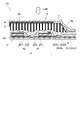
図1は、本実施の形態に係るX線検出器1を例示するための模式斜視図である。
なお、煩雑となるのを避けるために、図1においては、保護層2f、反射部4、防湿部5、および接着部6などを省いて描いている。
図2は、X線検出モジュール10を例示するための模式断面図である。
図3は、X線検出器1のブロック図である。
(
FIG. 1 is a schematic perspective view for illustrating an
In order to avoid complication, FIG. 1 omits the
FIG. 2 is a schematic cross-sectional view for illustrating the
FIG. 3 is a block diagram of the
図1および図2に示すように、X線検出器1には、X線検出モジュール10、および回路基板11を設けることができる。また、X線検出器1には、図示しない筐体を設けることができる。筐体の内部には、X線検出モジュール10、および回路基板11を設けることができる。例えば、筐体の内部に板状の支持板を設け、支持板のX線の入射側の面にはX線検出モジュール10を設け、支持板のX線の入射側とは反対側の面には回路基板11を設けることができる。
As shown in FIGS. 1 and 2, the
X線検出モジュール10には、アレイ基板2、シンチレータ3、反射部4、防湿部5、接着部6、および、吸光部7を設けることができる。
アレイ基板2には、基板2a、光電変換部2b、制御ライン(又はゲートライン)2c1、データライン(又はシグナルライン)2c2、配線パッド2d1、配線パッド2d2および保護層2fを設けることができる。
なお、光電変換部2b、制御ライン2c1、およびデータライン2c2の数などは例示をしたものに限定されるわけではない。
The
The
Note that the numbers of
基板2aは、板状を呈し、無アルカリガラスなどのガラスから形成することができる。基板2aの平面形状は、四角形とすることができる。基板2aの厚みは、例えば、0.7mm程度とすることができる。
光電変換部2bは、基板2aの一方の面側に複数設けることができる。光電変換部2bは、矩形状を呈し、制御ライン2c1とデータライン2c2とにより画された領域に設けることができる。複数の光電変換部2bは、マトリクス状に並べることができる。なお、1つの光電変換部2bは、例えば、X線画像の1つの画素(pixel)に対応する。
The
A plurality of
複数の光電変換部2bのそれぞれには、光電変換素子2b1と、スイッチング素子である薄膜トランジスタ(TFT;Thin Film Transistor)2b2を設けることができる。また、光電変換素子2b1において変換した信号電荷を蓄積する図示しない蓄積キャパシタを設けることができる。蓄積キャパシタは、例えば、矩形平板状を呈し、各薄膜トランジスタ2b2の下に設けることができる。ただし、光電変換素子2b1の容量によっては、光電変換素子2b1が蓄積キャパシタを兼ねることができる。
Each of the plurality of
光電変換素子2b1は、例えば、フォトダイオードなどとすることができる。
薄膜トランジスタ2b2は、蓄積キャパシタへの電荷の蓄積および放出のスイッチングを行うことができる。薄膜トランジスタ2b2は、ゲート電極2b2a、ドレイン電極2b2b及びソース電極2b2cを有することができる。薄膜トランジスタ2b2のゲート電極2b2aは、対応する制御ライン2c1と電気的に接続することができる。薄膜トランジスタ2b2のドレイン電極2b2bは、対応するデータライン2c2と電気的に接続することができる。薄膜トランジスタ2b2のソース電極2b2cは、対応する光電変換素子2b1と蓄積キャパシタとに電気的に接続することができる。また、光電変換素子2b1のアノード側と蓄積キャパシタは、グランドに電気的に接続することができる。なお、光電変換素子2b1のアノード側と蓄積キャパシタは、図示しないバイアスラインに電気的に接続することもできる。
The photoelectric conversion element 2b1 can be, for example, a photodiode.
The thin film transistor 2b2 is capable of switching charge storage and discharge to and from the storage capacitor. The thin film transistor 2b2 can have a gate electrode 2b2a, a drain electrode 2b2b and a source electrode 2b2c. Gate electrode 2b2a of thin film transistor 2b2 can be electrically connected to corresponding control line 2c1. Drain electrode 2b2b of thin film transistor 2b2 can be electrically connected to corresponding data line 2c2. The source electrode 2b2c of the thin film transistor 2b2 can be electrically connected to the corresponding photoelectric conversion element 2b1 and storage capacitor. Also, the anode side of the photoelectric conversion element 2b1 and the storage capacitor can be electrically connected to the ground. The anode side of the photoelectric conversion element 2b1 and the storage capacitor can also be electrically connected to a bias line (not shown).
制御ライン2c1は、所定の間隔をあけて互いに平行に複数設けることができる。制御ライン2c1は、例えば、行方向に延びるものとすることができる。
1つの制御ライン2c1は、基板2aの周縁近傍に設けられた複数の配線パッド2d1のうちの1つと電気的に接続することができる。1つの配線パッド2d1には、フレキシブルプリント基板2e1に設けられた複数の配線のうちの1つを電気的に接続することができる。フレキシブルプリント基板2e1に設けられた複数の配線の他端は、回路基板11に設けられた読み出し回路11aとそれぞれ電気的に接続することができる。
A plurality of control lines 2c1 can be provided parallel to each other at predetermined intervals. The control line 2c1 can extend, for example, in the row direction.
One control line 2c1 can be electrically connected to one of a plurality of wiring pads 2d1 provided near the periphery of the
データライン2c2は、所定の間隔をあけて互いに平行に複数設けることができる。データライン2c2は、例えば、行方向に直交する列方向に延びるものとすることができる。1つのデータライン2c2は、基板2aの周縁近傍に設けられた複数の配線パッド2d2のうちの1つと電気的に接続することができる。1つの配線パッド2d2には、フレキシブルプリント基板2e2に設けられた複数の配線のうちの1つを電気的に接続することができる。フレキシブルプリント基板2e2に設けられた複数の配線の他端は、回路基板11に設けられた信号検出回路11bとそれぞれ電気的に接続することができる。
制御ライン2c1、およびデータライン2c2は、例えば、アルミニウムやクロムなどの低抵抗金属を用いて形成することができる。
A plurality of data lines 2c2 can be provided parallel to each other at predetermined intervals. The data line 2c2 can extend, for example, in the column direction orthogonal to the row direction. One data line 2c2 can be electrically connected to one of a plurality of wiring pads 2d2 provided near the periphery of the
Control line 2c1 and data line 2c2 can be formed using, for example, a low-resistance metal such as aluminum or chromium.
保護層2fは、第1層2f1および第2層2f2を有することができる。第1層2f1は、光電変換部2b、制御ライン2c1、およびデータライン2c2を覆うことができる。第2層2f2は、第1層2f1の上に設けることができる。
第1層2f1および第2層2f2は、絶縁性材料から形成することができる。絶縁性材料は、例えば、酸化物絶縁材料、窒化物絶縁材料、酸窒化物絶縁材料、および樹脂などとすることができる。
The
The first layer 2f1 and the second layer 2f2 can be formed from an insulating material. The insulating material can be, for example, an oxide insulating material, a nitride insulating material, an oxynitride insulating material, a resin, or the like.
シンチレータ3は、複数の光電変換部2bの上に設けられ、入射するX線を蛍光すなわち可視光に変換することができる。シンチレータ3は、基板2a上の、複数の光電変換部2bが設けられた領域(有効画素領域A)を覆うように設けることができる。
The
シンチレータ3は、例えば、ヨウ化セシウム(CsI):タリウム(Tl)、ヨウ化ナトリウム(NaI):タリウム(Tl)、あるいは臭化セシウム(CsBr):ユーロピウム(Eu)などを用いて形成することができる。シンチレータ3は、真空蒸着法を用いて形成することができる。真空蒸着法を用いてシンチレータ3を形成すれば、複数の柱状結晶の集合体からなるシンチレータ3が形成される。
The
なお、真空蒸着法を用いてシンチレータ3を形成する際には、開口を有するマスクを用いることができる。この場合、アレイ基板2上の開口に対峙する位置(有効画素領域Aの上)にシンチレータ3を形成することができる。また、蒸着による膜は、マスクの表面にも形成される。そして、マスクの開口の近傍においては、膜は、開口の内部に徐々に張り出すように成長する。開口の内部に膜が張り出すと、開口の近傍において、アレイ基板2への蒸着が抑制される。そのため、図1および図2に示すように、シンチレータ3の周縁近傍は、外側になるに従い厚みが漸減している。
When forming the
また、シンチレータ3は、例えば、テルビウム賦活硫酸化ガドリニウム(Gd2O2S/Tb、又はGOS)などを用いて形成することもできる。この場合、複数の光電変換部2bごとに四角柱状のシンチレータ3が設けられるように、マトリクス状の溝部を設けることができる。
The
反射部4は、蛍光の利用効率を高めて感度特性を改善するために設けることができる。すなわち、反射部4は、シンチレータ3において生じた蛍光のうち、光電変換部2bが設けられた側とは反対側に向かう光を反射させて、光電変換部2bに向かうようにすることができる。ただし、反射部4は、必ずしも必要ではなく、X線検出モジュール10に求められる感度特性などに応じて設けるようにすればよい。
以下においては、一例として、反射部4が設けられる場合を説明する。
The
In the following, as an example, a case where the reflecting
反射部4は、シンチレータ3の上に設けることができる。反射部4は、シンチレータ3のX線の入射側に設けることができる。反射部4は、例えば、シンチレータ3の上面3aの、有効画素領域Aと対峙する領域を覆うように設けることができる。反射部4は、例えば、酸化チタン(TiO2)などからなる光散乱性粒子と、樹脂と、溶媒とを混合した材料をシンチレータ3上に塗布し、これを乾燥させることで形成することができる。
The
また、例えば、銀合金やアルミニウムなどの光反射率の高い金属からなる層をシンチレータ3上に成膜することで反射部4を形成することができる。また、例えば、表面が銀合金やアルミニウムなどの光反射率の高い金属からなるシートや、光散乱性粒子を含む樹脂シートなどをシンチレータ3上に接合することで反射部4とすることもできる。この場合、例えば、両面テープなどを用いて、シートとシンチレータ3とを接合することができる。
Further, for example, the
防湿部5は、空気中に含まれる水分により、反射部4の特性やシンチレータ3の特性が劣化するのを抑制するために設けることができる。防湿部5は、シンチレータ3および吸光部7を覆うものとすることができる。反射部4が設けられる場合には、防湿部5は、シンチレータ3、反射部4、および吸光部7を覆うものとすることができる。防湿部5と反射部4などとの間には隙間があってもよいし、防湿部5と反射部4などとが接触するようにしてもよい。例えば、大気圧よりも減圧された環境において防湿部5の周縁近傍とアレイ基板2とを接着すれば、防湿部5と反射部4などとが接触するようにすることができる。
The moisture-
防湿部5は、透湿係数の小さい材料から形成することができる。防湿部5は、例えば、金属を含むものとすることができる。防湿部5は、例えば、銅を含む金属、アルミニウムを含む金属、ステンレス、コバール材などの金属から形成することができる。防湿部5は、例えば、樹脂膜と金属膜とが積層された積層膜から形成することもできる。この場合、樹脂膜は、例えば、ポリイミド樹脂、エポキシ樹脂、ポリエチレンテレフタレート樹脂、テフロン(登録商標)、低密度ポリエチレン、高密度ポリエチレン、弾性ゴムなどから形成されたものとすることができる。金属膜は、例えば、銅を含む金属、アルミニウムを含む金属、ステンレス、コバール材などの金属から形成されたものとすることができる。この場合、金属を含む防湿部5とすれば、防湿部5を透過する水分をほぼ完全になくすことができる。
The moisture-
また、防湿部5の厚みは、X線の吸収や剛性などを考慮して決定することができる。この場合、防湿部5の厚みを厚くしすぎるとX線の吸収が大きくなりすぎる。防湿部5の厚みを薄くしすぎると剛性が低下して破損しやすくなる。防湿部5は、例えば、厚みが0.1mmのアルミニウム箔を用いて形成することができる。
Also, the thickness of the moisture-
図2に示すように、接着部6は、防湿部5の周縁近傍とアレイ基板2との間に設けることができる。接着部6は、防湿部5の周縁近傍とアレイ基板2とを接着している。接着部6は、例えば、紫外線硬化型接着剤や二液混合型接着剤などが硬化することで形成されたものとすることができる。
As shown in FIG. 2 , the
図1に示すように、回路基板11は、アレイ基板2の、シンチレータ3が設けられる側とは反対側に設けることができる。回路基板11は、X線検出モジュール10(アレイ基板2)と電気的に接続することができる。
図3に示すように、回路基板11には、読み出し回路11aおよび信号検出回路11bを設けることができる。なお、これらの回路を1つの基板に設けることもできるし、これらの回路を複数の基板に分けて設けることもできる。
As shown in FIG. 1, the
As shown in FIG. 3, the
読み出し回路11aは、薄膜トランジスタ2b2のオン状態とオフ状態を切り替えることができる。読み出し回路11aは、複数のゲートドライバ11aaと行選択回路11abとを有することができる。
The
行選択回路11abには、X線検出器1の外部に設けられた図示しない画像処理部などから制御信号S1を入力することができる。行選択回路11abは、X線画像の走査方向に従って、対応するゲートドライバ11aaに制御信号S1を入力することができる。
A control signal S1 can be input to the row selection circuit 11ab from an image processing unit (not shown) provided outside the
ゲートドライバ11aaは、対応する制御ライン2c1に制御信号S1を入力することができる。例えば、読み出し回路11aは、フレキシブルプリント基板2e1を介して、制御信号S1を各制御ライン2c1毎に順次入力することができる。制御ライン2c1に入力された制御信号S1により薄膜トランジスタ2b2がオン状態となり、蓄積キャパシタから電荷(画像データ信号S2)を読み出すことができるようになる。
The gate driver 11aa can input the control signal S1 to the corresponding control line 2c1. For example, the
信号検出回路11bは、複数の積分アンプ11ba、複数の選択回路11bb、および複数のADコンバータ11bcを有することができる。
1つの積分アンプ11baは、1つのデータライン2c2と電気的に接続することができる。積分アンプ11baは、光電変換部2bからの画像データ信号S2を順次受信することができる。そして、積分アンプ11baは、一定時間内に流れる電流を積分し、その積分値に対応した電圧を選択回路11bbへ出力することができる。この様にすれば、所定の時間内にデータライン2c2を流れる電流の値(電荷量)を電圧値に変換することができる。すなわち、積分アンプ11baは、シンチレータ3において発生した蛍光の強弱分布に対応した画像データ情報を、電位情報へと変換することができる。
The signal detection circuit 11b can have multiple integration amplifiers 11ba, multiple selection circuits 11bb, and multiple AD converters 11bc.
One integrating amplifier 11ba can be electrically connected to one data line 2c2. The integrating amplifier 11ba can sequentially receive the image data signal S2 from the
選択回路11bbは、読み出しを行う積分アンプ11baを選択し、電位情報へと変換された画像データ信号S2を順次読み出すことができる。
ADコンバータ11bcは、読み出された画像データ信号S2をデジタル信号に順次変換することができる。デジタル信号に変換された画像データ信号S2は、配線を介して画像処理部に入力することができる。なお、デジタル信号に変換された画像データ信号S2は、無線により画像処理部に送信されるようにしてもよい。
The selection circuit 11bb can select the integrating amplifier 11ba to be read out and sequentially read out the image data signal S2 converted into potential information.
The AD converter 11bc can sequentially convert the read image data signal S2 into a digital signal. The image data signal S2 converted into a digital signal can be input to the image processing section via wiring. The image data signal S2 converted into a digital signal may be wirelessly transmitted to the image processing section.
画像処理部は、デジタル信号に変換された画像データ信号S2に基づいてX線画像を構成することができる。なお、画像処理部は、回路基板11と一体化することもできる。
The image processing section can construct an X-ray image based on the image data signal S2 converted into a digital signal. Note that the image processing section can also be integrated with the
ここで、前述したように、シンチレータ3は、真空蒸着法を用いて有効画素領域Aの上に形成したり、有効画素領域Aの上に材料を塗布したりして形成される。そのため、有効画素領域Aの上のみにシンチレータ3を形成することは難しい。すなわち、有効画素領域Aとシンチレータ3との間には、位置合わせ精度によるズレがある。この場合、有効画素領域Aの周縁近傍が、シンチレータ3の外側に設けられないようにするためには、平面視における寸法が、有効画素領域Aよりも大きいシンチレータ3とすればよい。そのため、一般的には、図2に示すように、シンチレータ3は、有効画素領域Aの外側の近傍にも設けられている。
Here, as described above, the
また、X線検出器1に入射するX線は、X線が照射される被写体の大きさに応じて照射領域が設定される。そのため、有効画素領域Aの外側にもX線が照射されることがある。
In addition, the X-rays incident on the
シンチレータ3に入射したX線は、シンチレータ3によって蛍光に変換される。
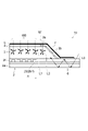
図4は、蛍光が発生する様子を例示するための模式断面図である。
図4に示すように、有効画素領域Aの上方に入射したX線100により発生した蛍光L1は、蛍光L1の下方に位置する光電変換部2b(光電変換素子2b1)に入射し、電荷に変換される。一方、有効画素領域Aの外側の上方に入射したX線101により発生した蛍光L2は、蛍光L2の下方に光電変換部2b(光電変換素子2b1)がない。そのため、蛍光L2は、電荷に変換されず散乱する。散乱した蛍光L2の一部は、シンチレータ3の側面3bや上面3aにおいて反射され、有効画素領域Aに照射される場合がある。
X-rays incident on the
FIG. 4 is a schematic cross-sectional view for illustrating how fluorescence is generated.
As shown in FIG. 4, the fluorescence L1 generated by the
また、X線検出器1が設けられる筐体の内部には動作確認用の発光ダイオードなどが設けられている。また、筐体の微細な隙間から筐体の内部に外光が入射する場合もある。前述したように、基板2aは、ガラスから形成されている。そのため、図4に示すように、発光ダイオードから出射した光や外光などの光L3が、基板2aを介して、シンチレータ3の内部に侵入する場合がある。シンチレータ3の内部に侵入した光L3は、シンチレータ3の側面3bや上面3aにおいて反射され、有効画素領域Aに照射される場合がある。
In addition, a light-emitting diode for operation confirmation and the like are provided inside the housing in which the
そのため、蛍光L2や光L3が発生すると、光電変換素子2b1の上方で発生した蛍光L1と、蛍光L2や光L3とが混合して光電変換素子2b1に入射するおそれがある。 Therefore, when the fluorescence L2 or the light L3 is generated, there is a possibility that the fluorescence L1 generated above the photoelectric conversion element 2b1 and the fluorescence L2 or the light L3 are mixed and enter the photoelectric conversion element 2b1.
また、人体に対して大量のX線照射を行うと健康への悪影響があるため、人体へのX線照射量は必要最低限に抑えられる。そのため、X線検出器1に入射するX線の強度は非常に小さいものとなり、シンチレータ3において発生する蛍光の強度が非常に小さくなる。そのため、X線検出器1に設けられる光電変換素子2b1は非常に高感度なものとされている。その結果、蛍光L2や光L3が、光電変換素子2b1により電荷に変換されやすくなる。
In addition, exposure of a large amount of X-rays to the human body has adverse effects on health, so the amount of X-rays irradiated to the human body is kept to a necessary minimum. Therefore, the intensity of the X-rays incident on the
蛍光L2や光L3による成分が混入した画像データ信号S2から構成されたX線画像は、これらが混入していない画像データ信号S2から構成されたX線画像に比べて、画像コントラストが低くなったり、画像ノイズが増加したりして、画像品質が悪くなるおそれがある。 The X-ray image composed of the image data signal S2 mixed with the components of the fluorescence L2 and the light L3 has a lower image contrast than the X-ray image composed of the image data signal S2 not mixed with these components. , image noise may increase and image quality may deteriorate.
そこで、本実施の形態に係るX線検出器1には、吸光部7が設けられている。
図1、図2、および図4に示すように、吸光部7は、シンチレータ3の上に設けることができる。平面視において、吸光部7は、有効画素領域Aの外側に設けることができる。例えば、吸光部7は、シンチレータ3の側面3bに設けることができる。また、反射部4が設けられる場合には、吸光部7は、平面視において、反射部4の外側に設けることができる。例えば、吸光部7は、シンチレータ3の上面3aにおける反射部4の外側、および、シンチレータ3の側面3bに設けることができる。
Therefore, the
As shown in FIGS. 1, 2, and 4, the
吸光部7は、可視光を吸収可能なものとすることができる。吸光部7は、可視光を吸収可能な色を有することができる。この場合、吸光部7の色は、例えば、黒色、または、黒色に近似する色とすることが好ましい。吸光部7の色が、黒色、または、黒色に近似する色であれば、前述した蛍光L2や光L3を吸収するのが容易となる。。黒色に近似する色は、例えば、黒と青の混色(例えば、紺色)、黒と赤の混色(例えば、茶色)などとすることができる。
The
吸光部7の色を黒とする場合には、吸光部7は、例えば、炭素系黒色顔料や酸化物系黒色顔料などを含むものとすることができる。炭素系黒色顔料は、例えば、カーボンブラックやグラファイトなどとすることができる。酸化物系黒色顔料は、例えば、鉄の酸化物、銅とクロムの複合酸化物、銅とクロムと亜鉛の複合酸化物などとすることができる。
When the color of the
吸光部7の厚みには特に限定がない。吸光部7の厚みは、例えば、1μm程度とすることができる。
The thickness of the
吸光部7は、例えば、黒色または黒色に近似する色の顔料、樹脂、および溶媒を混合した材料をシンチレータ3の表面に塗布し、これを乾燥させることで形成することができる。
また、吸光部7は、シンチレータ3の表面に紫外線などを照射し、シンチレータ3の表面を、例えば、茶色などに変色させることで形成することもできる。
The
Alternatively, the
前述した蛍光L2や光L3が吸光部7に入射すると、蛍光L2や光L3の一部が吸光部7に吸収される。そのため、蛍光L2や光L3が発生したとしても、光電変換素子2b1に入射する蛍光L2や光L3の量を少なくすることができる。その結果、画像コントラストが低くなったり、画像ノイズが増加したりするのを抑制することができるので、画像品質の向上を図ることができる。
When the fluorescence L2 and the light L3 described above enter the
(X線検出モジュール10の製造方法、およびX線検出器1の製造方法)
まず、基板2aの上に、制御ライン2c1、データライン2c2、配線パッド2d1、配線パッド2d2、光電変換部2b、および保護層2fなどを順次形成してアレイ基板2を製造する。アレイ基板2は、例えば、半導体製造プロセスを用いて製造することができる。なお、アレイ基板2の製造には既知の技術を適用することができるので詳細な説明は省略する。
(Method for Manufacturing
First, the
次に、基板2aの有効画素領域Aを覆うようにシンチレータ3を形成する。
例えば、シンチレータ3は、真空蒸着法を用いて形成することができる。真空蒸着法を用いてシンチレータ3を形成すれば、複数の柱状結晶の集合体からなるシンチレータ3が形成される。シンチレータ3の厚みは、X線検出器1に求められるDQE特性、感度特性、解像度特性などに応じて適宜変更することができる。シンチレータ3の厚みは、例えば、600μm程度とすることができる。
Next, a
For example, the
また、発光物質とバインダ材とを混合し、混合した材料を有効画素領域Aを覆うように塗布し、これを焼成し、焼成された材料にマトリクス状の溝部を形成して複数の光電変換部2bごとに四角柱状のシンチレータ3が設けられるようにしてもよい。
In addition, a light-emitting substance and a binder material are mixed, the mixed material is applied so as to cover the effective pixel region A, and the mixture is baked. A square prism-shaped
次に、必要に応じて、シンチレータ3の上に反射部4を形成する。
例えば、反射部4は、複数の光散乱性粒子、樹脂、および溶媒を混合した材料をシンチレータ3上に塗布し、これを乾燥させることで形成することができる。また、例えば、光反射率の高い金属からなる層をシンチレータ3上に成膜したり、光散乱性粒子を含む樹脂シートなどをシンチレータ3上に接合したりして、反射部4を形成することもできる。
Next, a
For example, the reflecting
次に、シンチレータ3の上に吸光部7を形成する。
例えば、吸光部7は、平面視において、シンチレータ3の表面の、有効画素領域Aの外側に位置する領域に、顔料、樹脂、および溶媒を混合した材料を塗布し、これを乾燥させることで形成することができる。
また、吸光部7は、シンチレータ3の表面に紫外線などを照射し、シンチレータ3の表面を、例えば、茶色などに変色させることで形成することもできる。
Next, a
For example, the
Alternatively, the
次に、シンチレータ3および吸光部7を覆うように防湿部5を設ける。反射部4が設けられる場合には、シンチレータ3、反射部4、および吸光部7を覆うように防湿部5を設ける。例えば、シート状またはハット状の防湿部5の周縁近傍をアレイ基板2に接着することができる。この場合、接着剤が硬化することで、接着部6が形成される。
Next, the moisture-
大気圧よりも減圧された環境において防湿部5をアレイ基板2に接着すれば、防湿部5の内部に水蒸気を含む空気が収納されるのを抑制することができる。また、航空機によりX線検出器1を輸送する場合などのように、X線検出器1が大気圧よりも減圧された環境に置かれる場合であっても、防湿部5の内部にある空気により防湿部5が膨張したり変形したりするのを抑制することができる。また、大気圧により防湿部5が押さえつけられるので、防湿部5がシンチレータ3などに密着する。
以上の様にして、X線検出モジュール10を製造することができる。
By adhering the moisture-
As described above, the
次に、フレキシブルプリント基板2e1、2e2を介して、アレイ基板2と回路基板11を電気的に接続する。
その他、回路部品などを適宜実装する。
Next, the
In addition, circuit parts and the like are mounted as appropriate.
次に、図示しない筐体の内部にアレイ基板2、回路基板11などを格納する。
そして、必要に応じて、光電変換素子2b1の異常の有無や電気的な接続の異常の有無を確認する電気試験、X線画像試験などを行う。
以上のようにして、X線検出器1を製造することができる。
なお、製品の防湿信頼性や温度環境の変化に対する信頼性を確認するために、高温高湿試験、冷熱サイクル試験などを実施することもできる。
Next, the
Then, if necessary, an electrical test, an X-ray image test, or the like is performed to confirm whether or not there is an abnormality in the photoelectric conversion element 2b1 and whether or not there is an abnormality in electrical connection.
As described above, the
In addition, in order to confirm the moisture-proof reliability of the product and the reliability against changes in the temperature environment, it is also possible to carry out a high-temperature and high-humidity test, a thermal cycle test, and the like.
以上に説明したように、本実施の形態に係るX線検出モジュール10の製造方法は以下の工程を備えることができる。
複数の光電変換部2bが設けられた領域(有効画素領域A)を覆い、平面視における寸法が、複数の光電変換部2bが設けられた領域よりも大きいシンチレータ3を形成する工程。
シンチレータ3の上に、可視光を吸収可能な吸光部7を形成する工程。
この場合、平面視において、吸光部7は、複数の光電変換部2bが設けられた領域の外側に形成される。
As described above, the method for manufacturing the
A step of forming a
A step of forming a
In this case, in plan view, the
吸光部7を形成する際に、シンチレータ3の表面に紫外線を照射し、シンチレータ3の表面を変色させることができる。
吸光部7を形成する際に、顔料を含む材料をシンチレータ3の表面に塗布することができる。
When forming the
A material containing a pigment can be applied to the surface of the
以上、本発明のいくつかの実施形態を例示したが、これらの実施形態は、例として提示したものであり、発明の範囲を限定することは意図していない。これら新規な実施形態は、その他の様々な形態で実施されることが可能であり、発明の要旨を逸脱しない範囲で、種々の省略、置き換え、変更などを行うことができる。これら実施形態やその変形例は、発明の範囲や要旨に含まれるとともに、特許請求の範囲に記載された発明とその均等の範囲に含まれる。また、前述の各実施形態は、相互に組み合わせて実施することができる。 Although some embodiments of the present invention have been illustrated above, these embodiments are presented by way of example and are not intended to limit the scope of the invention. These novel embodiments can be implemented in various other forms, and various omissions, replacements, changes, etc. can be made without departing from the scope of the invention. These embodiments and their modifications are included in the scope and gist of the invention, and are included in the scope of the invention described in the claims and equivalents thereof. Moreover, each of the above-described embodiments can be implemented in combination with each other.
1 X線検出器、2 アレイ基板、2a 基板、2b 光電変換部、2b1 光電変換素子、3 シンチレータ、3a 上面、3b 側面、7 吸光部、10 X線検出モジュール、11 回路基板
1
Claims (1)
前記シンチレータの上に、可視光を吸収可能な吸光部を形成する工程と、
を備え、
平面視において、前記吸光部は、前記複数の光電変換部が設けられた領域の外側に形成され、
前記吸光部を形成する際に、前記シンチレータの表面に紫外線を照射し、前記シンチレータの表面を変色させる放射線検出モジュールの製造方法。 a step of forming a scintillator covering a region provided with a plurality of photoelectric conversion units and having a dimension in plan view larger than the region provided with the plurality of photoelectric conversion units;
forming a light absorbing portion capable of absorbing visible light on the scintillator;
with
In plan view, the light absorbing portion is formed outside a region in which the plurality of photoelectric conversion portions are provided ,
A method of manufacturing a radiation detection module, wherein the surface of the scintillator is irradiated with ultraviolet rays to discolor the surface of the scintillator when the light absorbing portion is formed .
Priority Applications (7)
| Application Number | Priority Date | Filing Date | Title |
|---|---|---|---|
| JP2019184226A JP7199332B2 (en) | 2019-10-07 | 2019-10-07 | Method for manufacturing radiation detection module |
| KR1020227002626A KR102674545B1 (en) | 2019-10-07 | 2020-03-13 | Radiation detection module, radiation detector, and method of manufacturing radiation detection module |
| EP20875381.4A EP4043928A4 (en) | 2019-10-07 | 2020-03-13 | Radiation detection module, radiation detector, and method for manufacturing radiation detection module |
| PCT/JP2020/011049 WO2021070406A1 (en) | 2019-10-07 | 2020-03-13 | Radiation detection module, radiation detector, and method for manufacturing radiation detection module |
| CN202080057549.8A CN114270223A (en) | 2019-10-07 | 2020-03-13 | Radiation detection module, radiation detector, and method for manufacturing radiation detection module |
| TW109109920A TWI780420B (en) | 2019-10-07 | 2020-03-25 | Radiation detection module, radiation detector, and manufacturing method of radiation detection module |
| US17/667,754 US20220163682A1 (en) | 2019-10-07 | 2022-02-09 | Radiation detection module, radiation detector, and method for manufacturing radiation detection module |
Applications Claiming Priority (1)
| Application Number | Priority Date | Filing Date | Title |
|---|---|---|---|
| JP2019184226A JP7199332B2 (en) | 2019-10-07 | 2019-10-07 | Method for manufacturing radiation detection module |
Publications (2)
| Publication Number | Publication Date |
|---|---|
| JP2021060258A JP2021060258A (en) | 2021-04-15 |
| JP7199332B2 true JP7199332B2 (en) | 2023-01-05 |
Family
ID=75379999
Family Applications (1)
| Application Number | Title | Priority Date | Filing Date |
|---|---|---|---|
| JP2019184226A Active JP7199332B2 (en) | 2019-10-07 | 2019-10-07 | Method for manufacturing radiation detection module |
Country Status (7)
| Country | Link |
|---|---|
| US (1) | US20220163682A1 (en) |
| EP (1) | EP4043928A4 (en) |
| JP (1) | JP7199332B2 (en) |
| KR (1) | KR102674545B1 (en) |
| CN (1) | CN114270223A (en) |
| TW (1) | TWI780420B (en) |
| WO (1) | WO2021070406A1 (en) |
Citations (4)
| Publication number | Priority date | Publication date | Assignee | Title |
|---|---|---|---|---|
| JP2011128085A (en) | 2009-12-18 | 2011-06-30 | Canon Inc | Radiographic imaging apparatus, radiographic imaging system, and method of manufacturing radiographic imaging apparatus |
| JP2014106022A (en) | 2012-11-26 | 2014-06-09 | Toray Ind Inc | Scintillator panel |
| JP2014122898A (en) | 2012-12-21 | 2014-07-03 | General Equipment For Medical Imaging Sa (Oncovision) | Gamma ray scintillation detector preserving original scintillation light distribution |
| JP2019052907A (en) | 2017-09-14 | 2019-04-04 | キヤノン株式会社 | Radiation detector and radiation detection system |
Family Cites Families (7)
| Publication number | Priority date | Publication date | Assignee | Title |
|---|---|---|---|---|
| JP4156709B2 (en) * | 1998-06-23 | 2008-09-24 | 浜松ホトニクス株式会社 | Scintillator panel, radiation image sensor and manufacturing method thereof |
| JP2007271504A (en) * | 2006-03-31 | 2007-10-18 | Toshiba Corp | Scintillator panel, planar detector and imaging apparatus |
| JP2008096344A (en) * | 2006-10-13 | 2008-04-24 | Canon Inc | Apparatus for detecting radiation and scintillator panel |
| JP4764407B2 (en) * | 2007-11-20 | 2011-09-07 | 東芝電子管デバイス株式会社 | Radiation detector and manufacturing method thereof |
| JP5905672B2 (en) * | 2011-06-28 | 2016-04-20 | 株式会社東芝 | Radiation detector and manufacturing method thereof |
| JP6725288B2 (en) * | 2016-03-30 | 2020-07-15 | 浜松ホトニクス株式会社 | Radiation detector manufacturing method |
| JP6715055B2 (en) * | 2016-03-30 | 2020-07-01 | 浜松ホトニクス株式会社 | Radiation detector and scintillator panel |
-
2019
- 2019-10-07 JP JP2019184226A patent/JP7199332B2/en active Active
-
2020
- 2020-03-13 EP EP20875381.4A patent/EP4043928A4/en active Pending
- 2020-03-13 CN CN202080057549.8A patent/CN114270223A/en active Pending
- 2020-03-13 WO PCT/JP2020/011049 patent/WO2021070406A1/en unknown
- 2020-03-13 KR KR1020227002626A patent/KR102674545B1/en active IP Right Grant
- 2020-03-25 TW TW109109920A patent/TWI780420B/en active
-
2022
- 2022-02-09 US US17/667,754 patent/US20220163682A1/en active Pending
Patent Citations (4)
| Publication number | Priority date | Publication date | Assignee | Title |
|---|---|---|---|---|
| JP2011128085A (en) | 2009-12-18 | 2011-06-30 | Canon Inc | Radiographic imaging apparatus, radiographic imaging system, and method of manufacturing radiographic imaging apparatus |
| JP2014106022A (en) | 2012-11-26 | 2014-06-09 | Toray Ind Inc | Scintillator panel |
| JP2014122898A (en) | 2012-12-21 | 2014-07-03 | General Equipment For Medical Imaging Sa (Oncovision) | Gamma ray scintillation detector preserving original scintillation light distribution |
| JP2019052907A (en) | 2017-09-14 | 2019-04-04 | キヤノン株式会社 | Radiation detector and radiation detection system |
Also Published As
| Publication number | Publication date |
|---|---|
| EP4043928A1 (en) | 2022-08-17 |
| TW202115427A (en) | 2021-04-16 |
| US20220163682A1 (en) | 2022-05-26 |
| CN114270223A (en) | 2022-04-01 |
| JP2021060258A (en) | 2021-04-15 |
| WO2021070406A1 (en) | 2021-04-15 |
| KR102674545B1 (en) | 2024-06-13 |
| EP4043928A4 (en) | 2023-11-01 |
| KR20220024975A (en) | 2022-03-03 |
| TWI780420B (en) | 2022-10-11 |
Similar Documents
| Publication | Publication Date | Title |
|---|---|---|
| KR101885016B1 (en) | Radiation detector and method for manufacturing same | |
| JP5693173B2 (en) | Radiation detection apparatus and radiation detection system | |
| EP3244236B1 (en) | Radiation detector and manufacturing method therefor | |
| JP2004317300A (en) | Plane radiation detector and its manufacturing method | |
| JP7199332B2 (en) | Method for manufacturing radiation detection module | |
| JP2020091236A (en) | Radiation detection module, radiation detector, and method for manufacturing radiation detection module | |
| JP6948815B2 (en) | Radiation detector | |
| JP2017203672A (en) | Radiation detector | |
| JP2017111082A (en) | Radiation detector and manufacturing method of the same | |
| US20200400843A1 (en) | Radiation detection panel, radiation detector, and method for manufacturing radiation detection panel | |
| JP6673600B2 (en) | Radiation detector and manufacturing method thereof | |
| JP6749038B2 (en) | Radiation detector and manufacturing method thereof | |
| JP6953186B2 (en) | Radiation detector | |
| JP6968668B2 (en) | Radiation detection module and radiation detector | |
| JP2014182002A (en) | Radiographic image detector | |
| JP2020041948A (en) | Radiation detection module, radiation detector, and method for manufacturing radiation detector | |
| JP2020056667A (en) | Radiation detection module, radiation detector, and method for manufacturing radiation detection module | |
| JP2017078648A (en) | Radiation detector | |
| JP2019039819A (en) | Radiation detector and manufacturing method thereof | |
| JP2021110666A (en) | Radiation detection module and radiation detector | |
| JP2023082795A (en) | Radiation detection panel and method for manufacturing radiation detection panel | |
| JP2020169879A (en) | Radiation detection module and radiation detector | |
| JP2020109365A (en) | Radiation detection module and radiation detector | |
| JP2018119849A (en) | Radiation detector, radiation detector manufacturing apparatus, and radiation detector manufacturing method |
Legal Events
| Date | Code | Title | Description |
|---|---|---|---|
| A621 | Written request for application examination |
Free format text: JAPANESE INTERMEDIATE CODE: A621 Effective date: 20220221 |
|
| A131 | Notification of reasons for refusal |
Free format text: JAPANESE INTERMEDIATE CODE: A131 Effective date: 20221104 |
|
| A521 | Request for written amendment filed |
Free format text: JAPANESE INTERMEDIATE CODE: A523 Effective date: 20221209 |
|
| TRDD | Decision of grant or rejection written | ||
| A01 | Written decision to grant a patent or to grant a registration (utility model) |
Free format text: JAPANESE INTERMEDIATE CODE: A01 Effective date: 20221216 |
|
| A61 | First payment of annual fees (during grant procedure) |
Free format text: JAPANESE INTERMEDIATE CODE: A61 Effective date: 20221220 |
|
| R150 | Certificate of patent or registration of utility model |
Ref document number: 7199332 Country of ref document: JP Free format text: JAPANESE INTERMEDIATE CODE: R150 |