JP2014182002A - Radiographic image detector - Google Patents
Radiographic image detector Download PDFInfo
- Publication number
- JP2014182002A JP2014182002A JP2013056554A JP2013056554A JP2014182002A JP 2014182002 A JP2014182002 A JP 2014182002A JP 2013056554 A JP2013056554 A JP 2013056554A JP 2013056554 A JP2013056554 A JP 2013056554A JP 2014182002 A JP2014182002 A JP 2014182002A
- Authority
- JP
- Japan
- Prior art keywords
- photoelectric conversion
- phosphor
- conversion panel
- layer
- image detection
- Prior art date
- Legal status (The legal status is an assumption and is not a legal conclusion. Google has not performed a legal analysis and makes no representation as to the accuracy of the status listed.)
- Pending
Links
- OAICVXFJPJFONN-UHFFFAOYSA-N Phosphorus Chemical compound [P] OAICVXFJPJFONN-UHFFFAOYSA-N 0.000 claims abstract description 156
- 238000006243 chemical reaction Methods 0.000 claims abstract description 111
- 238000005192 partition Methods 0.000 claims abstract description 63
- 229920005989 resin Polymers 0.000 claims abstract description 55
- 239000011347 resin Substances 0.000 claims abstract description 55
- 238000003384 imaging method Methods 0.000 claims abstract description 12
- 230000007423 decrease Effects 0.000 claims abstract description 6
- 239000010410 layer Substances 0.000 claims description 146
- 238000001514 detection method Methods 0.000 claims description 43
- 239000000758 substrate Substances 0.000 claims description 32
- 230000005855 radiation Effects 0.000 claims description 27
- 239000012790 adhesive layer Substances 0.000 claims description 25
- 239000002245 particle Substances 0.000 claims description 21
- 239000011230 binding agent Substances 0.000 claims description 18
- 230000035945 sensitivity Effects 0.000 abstract description 5
- 239000011159 matrix material Substances 0.000 abstract description 4
- 239000011800 void material Substances 0.000 abstract 2
- 239000010408 film Substances 0.000 description 39
- 239000000463 material Substances 0.000 description 16
- 238000012545 processing Methods 0.000 description 10
- 239000011248 coating agent Substances 0.000 description 9
- 238000000576 coating method Methods 0.000 description 9
- 239000013078 crystal Substances 0.000 description 9
- 239000011521 glass Substances 0.000 description 9
- 238000004519 manufacturing process Methods 0.000 description 9
- 230000001681 protective effect Effects 0.000 description 8
- 229910052782 aluminium Inorganic materials 0.000 description 7
- XAGFODPZIPBFFR-UHFFFAOYSA-N aluminium Chemical compound [Al] XAGFODPZIPBFFR-UHFFFAOYSA-N 0.000 description 7
- 230000000875 corresponding effect Effects 0.000 description 7
- 238000000034 method Methods 0.000 description 7
- 239000004065 semiconductor Substances 0.000 description 7
- 239000000126 substance Substances 0.000 description 7
- 230000004048 modification Effects 0.000 description 6
- 238000012986 modification Methods 0.000 description 6
- 238000003860 storage Methods 0.000 description 6
- 229910021417 amorphous silicon Inorganic materials 0.000 description 5
- 239000003990 capacitor Substances 0.000 description 5
- 238000011049 filling Methods 0.000 description 5
- 239000007788 liquid Substances 0.000 description 5
- 229910052751 metal Inorganic materials 0.000 description 5
- 239000002184 metal Substances 0.000 description 5
- 239000010409 thin film Substances 0.000 description 5
- 239000010419 fine particle Substances 0.000 description 4
- 238000007789 sealing Methods 0.000 description 4
- 229910052581 Si3N4 Inorganic materials 0.000 description 3
- YXFVVABEGXRONW-UHFFFAOYSA-N Toluene Chemical compound CC1=CC=CC=C1 YXFVVABEGXRONW-UHFFFAOYSA-N 0.000 description 3
- BTANRVKWQNVYAZ-UHFFFAOYSA-N butan-2-ol Chemical compound CCC(C)O BTANRVKWQNVYAZ-UHFFFAOYSA-N 0.000 description 3
- 230000001902 propagating effect Effects 0.000 description 3
- HQVNEWCFYHHQES-UHFFFAOYSA-N silicon nitride Chemical compound N12[Si]34N5[Si]62N3[Si]51N64 HQVNEWCFYHHQES-UHFFFAOYSA-N 0.000 description 3
- 239000004925 Acrylic resin Substances 0.000 description 2
- 229920000178 Acrylic resin Polymers 0.000 description 2
- 229920000049 Carbon (fiber) Polymers 0.000 description 2
- RYGMFSIKBFXOCR-UHFFFAOYSA-N Copper Chemical compound [Cu] RYGMFSIKBFXOCR-UHFFFAOYSA-N 0.000 description 2
- PXHVJJICTQNCMI-UHFFFAOYSA-N Nickel Chemical compound [Ni] PXHVJJICTQNCMI-UHFFFAOYSA-N 0.000 description 2
- GWEVSGVZZGPLCZ-UHFFFAOYSA-N Titan oxide Chemical compound O=[Ti]=O GWEVSGVZZGPLCZ-UHFFFAOYSA-N 0.000 description 2
- 238000000862 absorption spectrum Methods 0.000 description 2
- 230000008901 benefit Effects 0.000 description 2
- 239000007767 bonding agent Substances 0.000 description 2
- 239000004917 carbon fiber Substances 0.000 description 2
- 229910052802 copper Inorganic materials 0.000 description 2
- 239000010949 copper Substances 0.000 description 2
- 230000000694 effects Effects 0.000 description 2
- 229910001385 heavy metal Inorganic materials 0.000 description 2
- AMGQUBHHOARCQH-UHFFFAOYSA-N indium;oxotin Chemical compound [In].[Sn]=O AMGQUBHHOARCQH-UHFFFAOYSA-N 0.000 description 2
- VNWKTOKETHGBQD-UHFFFAOYSA-N methane Chemical compound C VNWKTOKETHGBQD-UHFFFAOYSA-N 0.000 description 2
- 239000000203 mixture Substances 0.000 description 2
- 239000011368 organic material Substances 0.000 description 2
- TWNQGVIAIRXVLR-UHFFFAOYSA-N oxo(oxoalumanyloxy)alumane Chemical compound O=[Al]O[Al]=O TWNQGVIAIRXVLR-UHFFFAOYSA-N 0.000 description 2
- RVTZCBVAJQQJTK-UHFFFAOYSA-N oxygen(2-);zirconium(4+) Chemical compound [O-2].[O-2].[Zr+4] RVTZCBVAJQQJTK-UHFFFAOYSA-N 0.000 description 2
- 230000035699 permeability Effects 0.000 description 2
- 238000000206 photolithography Methods 0.000 description 2
- 238000003825 pressing Methods 0.000 description 2
- 230000008569 process Effects 0.000 description 2
- -1 quinacridone organic compound Chemical class 0.000 description 2
- 238000005070 sampling Methods 0.000 description 2
- 238000007650 screen-printing Methods 0.000 description 2
- 239000002344 surface layer Substances 0.000 description 2
- OGIDPMRJRNCKJF-UHFFFAOYSA-N titanium oxide Inorganic materials [Ti]=O OGIDPMRJRNCKJF-UHFFFAOYSA-N 0.000 description 2
- 238000002834 transmittance Methods 0.000 description 2
- 229910001928 zirconium oxide Inorganic materials 0.000 description 2
- OKTJSMMVPCPJKN-UHFFFAOYSA-N Carbon Chemical compound [C] OKTJSMMVPCPJKN-UHFFFAOYSA-N 0.000 description 1
- 229910052684 Cerium Inorganic materials 0.000 description 1
- 229910052693 Europium Inorganic materials 0.000 description 1
- 229910052688 Gadolinium Inorganic materials 0.000 description 1
- 229910052765 Lutetium Inorganic materials 0.000 description 1
- CERQOIWHTDAKMF-UHFFFAOYSA-N Methacrylic acid Chemical compound CC(=C)C(O)=O CERQOIWHTDAKMF-UHFFFAOYSA-N 0.000 description 1
- CTQNGGLPUBDAKN-UHFFFAOYSA-N O-Xylene Chemical compound CC1=CC=CC=C1C CTQNGGLPUBDAKN-UHFFFAOYSA-N 0.000 description 1
- 229910052777 Praseodymium Inorganic materials 0.000 description 1
- 229910052772 Samarium Inorganic materials 0.000 description 1
- 229910052771 Terbium Inorganic materials 0.000 description 1
- 238000010521 absorption reaction Methods 0.000 description 1
- 239000000853 adhesive Substances 0.000 description 1
- 230000001070 adhesive effect Effects 0.000 description 1
- 239000003513 alkali Substances 0.000 description 1
- PNEYBMLMFCGWSK-UHFFFAOYSA-N aluminium oxide Inorganic materials [O-2].[O-2].[O-2].[Al+3].[Al+3] PNEYBMLMFCGWSK-UHFFFAOYSA-N 0.000 description 1
- 230000004888 barrier function Effects 0.000 description 1
- 229920005601 base polymer Polymers 0.000 description 1
- 230000005540 biological transmission Effects 0.000 description 1
- 230000015572 biosynthetic process Effects 0.000 description 1
- 239000002041 carbon nanotube Substances 0.000 description 1
- 229910021393 carbon nanotube Inorganic materials 0.000 description 1
- 239000000919 ceramic Substances 0.000 description 1
- GWXLDORMOJMVQZ-UHFFFAOYSA-N cerium Chemical compound [Ce] GWXLDORMOJMVQZ-UHFFFAOYSA-N 0.000 description 1
- 239000003795 chemical substances by application Substances 0.000 description 1
- 230000003081 coactivator Effects 0.000 description 1
- 238000004891 communication Methods 0.000 description 1
- 229910052878 cordierite Inorganic materials 0.000 description 1
- 238000012937 correction Methods 0.000 description 1
- 230000002596 correlated effect Effects 0.000 description 1
- 230000002950 deficient Effects 0.000 description 1
- 238000010586 diagram Methods 0.000 description 1
- 238000009792 diffusion process Methods 0.000 description 1
- JSKIRARMQDRGJZ-UHFFFAOYSA-N dimagnesium dioxido-bis[(1-oxido-3-oxo-2,4,6,8,9-pentaoxa-1,3-disila-5,7-dialuminabicyclo[3.3.1]nonan-7-yl)oxy]silane Chemical compound [Mg++].[Mg++].[O-][Si]([O-])(O[Al]1O[Al]2O[Si](=O)O[Si]([O-])(O1)O2)O[Al]1O[Al]2O[Si](=O)O[Si]([O-])(O1)O2 JSKIRARMQDRGJZ-UHFFFAOYSA-N 0.000 description 1
- 238000001035 drying Methods 0.000 description 1
- 239000003822 epoxy resin Substances 0.000 description 1
- 239000000945 filler Substances 0.000 description 1
- VOZRXNHHFUQHIL-UHFFFAOYSA-N glycidyl methacrylate Chemical compound CC(=C)C(=O)OCC1CO1 VOZRXNHHFUQHIL-UHFFFAOYSA-N 0.000 description 1
- 239000011810 insulating material Substances 0.000 description 1
- 229910052746 lanthanum Inorganic materials 0.000 description 1
- 238000009607 mammography Methods 0.000 description 1
- 239000012046 mixed solvent Substances 0.000 description 1
- 238000002156 mixing Methods 0.000 description 1
- QVEIBLDXZNGPHR-UHFFFAOYSA-N naphthalene-1,4-dione;diazide Chemical compound [N-]=[N+]=[N-].[N-]=[N+]=[N-].C1=CC=C2C(=O)C=CC(=O)C2=C1 QVEIBLDXZNGPHR-UHFFFAOYSA-N 0.000 description 1
- 229910052759 nickel Inorganic materials 0.000 description 1
- 239000004014 plasticizer Substances 0.000 description 1
- 229920002037 poly(vinyl butyral) polymer Polymers 0.000 description 1
- 229920000647 polyepoxide Polymers 0.000 description 1
- 230000009467 reduction Effects 0.000 description 1
- KZUNJOHGWZRPMI-UHFFFAOYSA-N samarium atom Chemical compound [Sm] KZUNJOHGWZRPMI-UHFFFAOYSA-N 0.000 description 1
- 238000003756 stirring Methods 0.000 description 1
- 229920002803 thermoplastic polyurethane Polymers 0.000 description 1
- 229920001187 thermosetting polymer Polymers 0.000 description 1
- 239000008096 xylene Substances 0.000 description 1
- 229910052727 yttrium Inorganic materials 0.000 description 1
- YVTHLONGBIQYBO-UHFFFAOYSA-N zinc indium(3+) oxygen(2-) Chemical compound [O--].[Zn++].[In+3] YVTHLONGBIQYBO-UHFFFAOYSA-N 0.000 description 1
Images


Abstract
Description
本発明は、間接変換方式の放射線画像検出装置に関する。 The present invention relates to an indirect conversion radiation image detection apparatus.
医療分野などにおいて、体内を観察するための放射線画像撮影システムが普及している。この放射線画像撮影システムは、放射線源から被写体に向けてX線などの放射線を放射する放射線源と、被写体を透過した放射線を検出して電荷に変換し、この電荷を電圧に変換して、被写体の放射線画像を表す画像データを生成する放射線画像検出装置とを備えている。 In the medical field and the like, a radiographic imaging system for observing the inside of a body is widespread. This radiographic imaging system detects a radiation source that emits radiation, such as X-rays, from a radiation source toward a subject, detects radiation that has passed through the subject, converts it into a charge, converts the charge into a voltage, And a radiological image detection device for generating image data representing the radiographic image of the above.
放射線画像検出装置には、放射線を直接電荷に変換する直接変換方式と、放射線を一旦可視光に変換し、この可視光を電荷に変換する間接変換方式がある。間接変換方式の放射線画像検出装置は、放射線を可視光に変換する蛍光体層(シンチレータ)と、この蛍光体層により生成された可視光を電荷に変換する光電変換パネルとを有する。光電変換パネルには、フォトダイオードを含む画素が2次元マトリクス状に複数配列されており、この上に蛍光体層が積層されている。 The radiation image detection apparatus includes a direct conversion system that directly converts radiation into electric charges and an indirect conversion system that converts radiation once into visible light and converts the visible light into electric charge. The indirect conversion type radiological image detection apparatus includes a phosphor layer (scintillator) that converts radiation into visible light, and a photoelectric conversion panel that converts visible light generated by the phosphor layer into electric charge. In the photoelectric conversion panel, a plurality of pixels including photodiodes are arranged in a two-dimensional matrix, and a phosphor layer is stacked thereon.
蛍光体層には、GOS(Gd2O2S:Tb)等の粒子状の蛍光体材料(粒状結晶)を有する粒状タイプと、CsI:Tlなどの柱状の蛍光体材料(柱状結晶)を有する柱状タイプとが知られている。 The phosphor layer has a granular type having a particulate phosphor material (granular crystal) such as GOS (Gd 2 O 2 S: Tb) and a columnar phosphor material (columnar crystal) such as CsI: Tl. A columnar type is known.
粒状タイプの蛍光体層は、GOS等の蛍光体粒子を樹脂などのバインダ(結合剤)に分散させて形成されるため、可撓性を有し、耐衝撃性に優れるといった利点がある。特に、GOSを有する蛍光体層は、GOSに含まれる重金属原子のGdが、CsIに含まれる重金属原子のCsより原子番号が大きいため、耐衝撃性に加えて、放射線の吸収率が高い。しかし、粒状タイプの蛍光体層では、蛍光体粒子から可視光が等方的に放射され、光ガイド効果を有さないため、画像の分解能が低い。放射線の変換効率を高めるには、蛍光体層の膜厚を大きくすればよいが、膜厚が大きいほど、可視光が光電変換パネルに到達するまでの間での拡散が大きく、分解能が低下する。 Since the granular type phosphor layer is formed by dispersing phosphor particles such as GOS in a binder (binder) such as a resin, there is an advantage that it has flexibility and excellent impact resistance. In particular, since the phosphor layer having GOS has a larger atomic number than Cs of heavy metal atoms contained in CsI, Gd of heavy metal atoms contained in GOS has a high radiation absorption rate in addition to impact resistance. However, in the granular type phosphor layer, visible light is isotropically radiated from the phosphor particles and has no light guide effect, so that the resolution of the image is low. In order to increase the conversion efficiency of radiation, the thickness of the phosphor layer may be increased. However, the larger the thickness, the greater the diffusion of visible light until it reaches the photoelectric conversion panel, resulting in a lower resolution. .
これに対して、柱状タイプの蛍光体層は、基板上に蛍光体材料を結晶成長させて柱状結晶としたものであり、各柱状結晶が光ガイド効果を有するため、画像の分解能が高い。しかし、柱状タイプの蛍光体層では、厚膜化を図ろうとすると、一部の柱状結晶が異常成長して突起が生じたり、隣接する柱状結晶同士が融着するといった欠陥が生じやすいため、厚膜化には限界がある。また、柱状タイプの蛍光体層は、柱状結晶を有することにより耐衝撃性が低い。さらに、柱状タイプの蛍光体層は、材料が高価であり、製造コストが嵩む。 On the other hand, the columnar type phosphor layer is a columnar crystal obtained by crystal growth of a phosphor material on a substrate. Since each columnar crystal has a light guide effect, the resolution of the image is high. However, in the columnar type phosphor layer, when trying to increase the film thickness, some columnar crystals are likely to grow abnormally and produce protrusions, and adjacent columnar crystals are likely to be fused together. There is a limit to film formation. In addition, the columnar type phosphor layer has a columnar crystal and has low impact resistance. Furthermore, the columnar type phosphor layer is expensive in material and increases in manufacturing cost.
そこで、粒状タイプの蛍光体層を有する放射線画像検出装置において、蛍光体層を各フォトダイオードに対応して分離する隔壁を設けることが提案されている(例えば、特許文献1〜3参照)。この隔壁には、各フォトダイオードに対応して開口部が設けられている。各開口部内の蛍光体で発生した可視光は、隔壁により拡散が防止され、対応するフォトダイオードに効率よく導かれるため、分解能が向上する。このような隔壁を有する粒状タイプの蛍光体層は、製造コスト、耐衝撃性、かつ分解能に優れる。
In view of this, it has been proposed that a radiation image detection apparatus having a granular type phosphor layer is provided with a partition that separates the phosphor layer in correspondence with each photodiode (see, for example,
特許文献1に記載の放射線画像検出装置では、隔壁の開口部の断面積(開口率)は、蛍光体層の厚さ方向に一定である。蛍光体層中に隔壁を設けると、その分だけ蛍光体層での発光量が低下するため、特許文献2、3に記載の放射線画像検出装置では、隔壁の光電変換パネル側の開口率を、光電変換パネルとは反対側の開口率より大きくすることにより、光電変換パネル側での蛍光体層の発光量を高めている。
In the radiological image detection apparatus described in
しかしながら、特許文献2、3に記載のように、隔壁の光電変換パネル側の開口率を大きくすると、その分だけ光電変換パネル側の隔壁の幅が薄くなり、破損しやすくなる。また、隔壁の高さにばらつきが生じやすくなるので、特許文献2に記載のように、隔壁の開口部に、蛍光体を充填することにより蛍光体層を形成した場合には、蛍光体層の光電変換パネル側の表面の平坦性が低く、凹凸が生じ、光電変換パネルと蛍光体層との間に空気層が生じる恐れがある。
However, as described in
光電変換パネルと蛍光体層との間に空気層が介在すると、蛍光体と空気層との間の屈折率差が生じ、蛍光体の屈折率が空気層の屈折率より大きいことにより、蛍光体から光電変換パネルに向かう可視光が、蛍光体と空気層との界面で反射されやすくなり、フォトダイオードへの可視光の入射効率が低下する(放射線画像検出装置の感度が低下する)という問題が生じる。 When an air layer is interposed between the photoelectric conversion panel and the phosphor layer, a refractive index difference between the phosphor and the air layer is generated, and the phosphor has a refractive index larger than the refractive index of the air layer. Visible light going from the light to the photoelectric conversion panel is easily reflected at the interface between the phosphor and the air layer, and the incident efficiency of visible light to the photodiode is reduced (the sensitivity of the radiation image detection device is reduced). Arise.
本発明は、製造コスト、耐衝撃性、分解能に優れ、感度の低下を防止することを可能とする放射線画像検出装置を提供することを目的とする。 An object of the present invention is to provide a radiological image detection apparatus that is excellent in manufacturing cost, impact resistance, and resolution, and that can prevent a decrease in sensitivity.
上記課題を解決するために、本発明の放射線画像検出装置は、光電変換を行うフォトダイオードを含む画素が2次元配列された撮像面を有する光電変換パネルと、隔壁と蛍光体とを備え、隔壁は、各フォトダイオードに対応して配置されるとともに、撮像面に平行な方向の断面積が、光電変換パネル側のほうが、光電変換パネルとは反対側より大きい開口部を有し、蛍光体は、各開口部内に、光電変換パネル側に空隙を残して充填され、放射線を可視光に変換する蛍光体層と、空隙に形成された樹脂層と、を備える。 In order to solve the above problems, a radiological image detection apparatus of the present invention includes a photoelectric conversion panel having an imaging surface in which pixels including photodiodes that perform photoelectric conversion are two-dimensionally arranged, a partition wall, and a phosphor. Is arranged corresponding to each photodiode, and the cross-sectional area in the direction parallel to the imaging surface has a larger opening on the photoelectric conversion panel side than the side opposite to the photoelectric conversion panel, and the phosphor is Each of the openings includes a phosphor layer that is filled with leaving a gap on the photoelectric conversion panel side and converts radiation into visible light, and a resin layer formed in the gap.
光電変換パネル及び蛍光体層は、放射線が入射する側から、光電変換パネル、蛍光体層の順番に配置されていることが好ましい。 It is preferable that the photoelectric conversion panel and the phosphor layer are arranged in the order of the photoelectric conversion panel and the phosphor layer from the side on which the radiation is incident.
蛍光体層は、樹脂層が形成された表面が、粘着層を介して光電変換パネルに貼り合わされているか、または、樹脂層が形成された表面が、光電変換パネルに直接当接していることが好ましい。 In the phosphor layer, the surface on which the resin layer is formed is bonded to the photoelectric conversion panel via the adhesive layer, or the surface on which the resin layer is formed is in direct contact with the photoelectric conversion panel. preferable.
各開口部は、光電変換パネルから離れる方向に次第に断面積が減少していることが好ましい。 It is preferable that the cross-sectional area of each opening gradually decreases in a direction away from the photoelectric conversion panel.
蛍光体層の光電変換パネルと反対側の表面に、可視光を反射する光反射層が形成されていることが好ましい。この場合、蛍光体層は、蛍光体支持基板上に、光反射層を介して形成されていることが好ましい。 A light reflecting layer that reflects visible light is preferably formed on the surface of the phosphor layer opposite to the photoelectric conversion panel. In this case, the phosphor layer is preferably formed on the phosphor support substrate via a light reflection layer.
蛍光体は、バインダと、このバインダに分散された蛍光体粒子とを含むことが好ましい。隔壁は、蛍光体より屈折率が低いことが好ましい。 The phosphor preferably includes a binder and phosphor particles dispersed in the binder. The barrier ribs preferably have a refractive index lower than that of the phosphor.
隔壁の光電変換パネル側の開口率が85%以上であることが好ましい。この場合、蛍光体層の厚みが400μm以上であることが好ましい。 It is preferable that the aperture ratio of the partition wall on the photoelectric conversion panel side is 85% or more. In this case, the thickness of the phosphor layer is preferably 400 μm or more.
本発明の放射線画像検出装置によれば、隔壁は、光電変換パネル側のほうが、光電変換パネルとは反対側より断面積が大きい開口部を有し、蛍光体は、各開口部内に、光電変換パネル側に空隙を残して充填され、この空隙に樹脂層が形成されているので、光電変換パネルと蛍光体との間に空気層が介在せず、感度の低下を防止することができる。 According to the radiation image detection apparatus of the present invention, the partition wall has an opening having a larger cross-sectional area on the photoelectric conversion panel side than on the side opposite to the photoelectric conversion panel, and the phosphor is photoelectrically converted in each opening. Since the panel side is filled with a gap, and a resin layer is formed in the gap, an air layer is not interposed between the photoelectric conversion panel and the phosphor, and a reduction in sensitivity can be prevented.
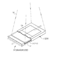
図1において、X線画像検出装置10は、フラットパネル検出器(FPD:Flat Panel Detector)11と、回路支持基板12と、制御ユニット13と、これらを収容する筐体14により構成されている。筐体14は、X線XRの透過性が高く、軽量で耐久性の高い炭素繊維強化樹脂(カーボンファイバー)により一体形成されたモノコック構造である。X線画像検出装置10は、可搬型の電子カセッテである。
In FIG. 1, an X-ray
筐体14の1つの側面には、開口部(図示せず)と、この開口部を塞ぐ蓋部材(図示せず)とが設けられている。X線画像検出装置10の製造時には、開口部からFPD11や制御ユニット13が筐体14内に挿入される。
One side surface of the
筐体14には、撮影時にX線源80(図8参照)から放射され、被写体(患者)81(図8参照)を透過したX線XRが照射される照射面14aが設けられている。この照射面14aには、被写体81の撮像可能領域とその中心位置とを示すガイド線15が形成されている。ガイド線15の外枠が、撮影可能領域に対応し、ガイド線15が十字状に交差する交点が撮影可能領域の中心位置に対応する。
The
筐体14内には、照射面14a側から順に、FPD11、回路支持基板12が配置されている。回路支持基板12は、回路基板30(図2参照)を支持しており、筐体14に固定されている。制御ユニット13は、筐体14内の短手方向に沿った一端側に配置されている。
In the
制御ユニット13は、マイクロコンピュータやバッテリ(いずれも図示せず)を収容している。このマイクロコンピュータは、有線または無線により、X線源80に接続されたコンソール(図示せず)と通信して、FPD11の動作を制御する。
The
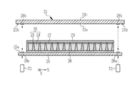
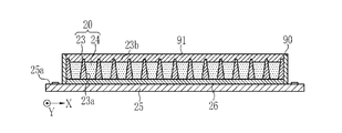
図2において、FPD11は、X線XRを可視光に変換する蛍光体層(シンチレータ)20と、この可視光を電荷に変換する光電変換パネル21を有している。X線画像検出装置10は、ISS(Irradiation Side Sampling)型であり、光電変換パネル21は、蛍光体層20よりX線XRの入射側に配置されている。蛍光体層20は、光電変換パネル21を透過したX線XRを可視光に変換して放出する。光電変換パネル21は、蛍光体層20から放出された可視光を光電変換して電荷に変換する。
In FIG. 2, the
光電変換パネル21は、筐体14の照射面14a側の内面に、エポキシ樹脂等からなる接着層22を介して貼り付けられている。光電変換パネル21の表面21aには、図3に示すように、光電変換を行うフォトダイオード(PD)43が、XY方向に沿って2次元マトリクス状に形成されている。表面21aのうち、PD43が配列された領域が撮像面である。
The
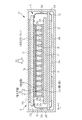
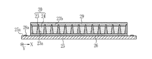
蛍光体層20は、図3に示すように平面形状が正方格子状で、かつ光電変換パネル21の各PD43に対応して開口部23aが設けられた隔壁23と、各開口部23a内に充填された蛍光体24とで構成されている。隔壁23は、ガラス微粒子とバインダとを主成分とするガラスペーストにより形成されている。隔壁23は、蛍光体24より屈折率が低く、蛍光体24から隔壁23に入射する可視光は、入射角が所定以上の場合に全反射する。また、隔壁23に、ガラス微粒子以外に、酸化チタン、酸化アルミニウム、酸化ジルコニウムなどのフィラー粒子を添加することにより、反射率を高めてもよい。
As shown in FIG. 3, the
蛍光体層20は、蛍光体支持基板25により支持されており、蛍光体層20と蛍光体支持基板25との間には、光反射膜26が形成されている。蛍光体支持基板25は、ガラス等の透明な絶縁性材料で形成されている。光反射膜26は、アルミニウム等の金属薄膜により形成されている。
The
隔壁23の各開口部23aは、平面形状がほぼPD43の形状に対応した四角形である。各開口部23aのXY面に平行な方向の断面積は、光電変換パネル21から離れる方向に次第に小さくなっている。蛍光体24は、各開口部23a内に、蛍光体支持基板25側から充填されており、光電変換パネル21側までは完全には満たされていない。この各開口部23aの光電変換パネル21側には、樹脂層27が充填されている。各蛍光体24は、テーパ状の4つの側面を有する四角錐台(オベリスク)形状である。
Each opening 23 a of the
各開口部23aは、蛍光体24と樹脂層27とで完全に満たされており、各開口部23a内には空気層は存在しない。また、樹脂層27は、隔壁23の光電変換パネル21側を保護している。
Each
樹脂層27の屈折率は、蛍光体24から光電変換パネル21側への可視光の射出効率を高める(樹脂層27の表面での反射を抑える)ために、蛍光体24の屈折率に近く、かつ蛍光体24の屈折率より低いことが好ましい。具体的には、蛍光体24の屈折率は、バインダ24aの屈折率が支配的であるため、樹脂層27の屈折率は、バインダ24aの屈折率に近く、かつバインダ24aの屈折率より低いことが好ましい。これにより、蛍光体24から樹脂層27への可視光の入射効率が向上する。
The refractive index of the
蛍光体支持基板25の蛍光体層20を支持する側の表面25aには、蛍光体層20及び光反射膜26の形成領域外に、2つの第1のアライメントマーク28aが形成されている。各第1のアライメントマーク28aは、アルミニウムやニッケル等の金属薄膜で形成されている。各第1のアライメントマーク28aの平面形状は、例えば十字状である。
Two first alignment marks 28 a are formed on the
蛍光体層20は、光反射膜26が形成された面とは反対側が、アクリル系接合剤等からなる粘着層29を介して光電変換パネル21の表面21aに貼り合わされている。光電変換パネル21の表面21aには、第1のアライメントマーク28aに対向する位置に、第2のアライメントマーク28bが形成されている。各第2のアライメントマーク28bは、アルミニウム等の金属薄膜により形成され、第1のアライメントマーク28aと同一形状でかつ同一サイズである。第1及び第2のアライメントマーク28a,28bは、蛍光体層20を光電変換パネル21に貼り合わせる際に、PD43と隔壁23とを位置合わせするために用いられる。
The
回路支持基板12は、蛍光体支持基板25のX線XRの入射側とは反対側に配置されている。回路支持基板12は、筐体14の側部14bにビス等で固着されている。回路支持基板12の蛍光体支持基板25とは反対側の下面12aには、回路基板30が接着剤等を介して固定されている。
The
回路基板30と光電変換パネル21とは、フレキシブルプリント基板31を介して電気的に接続されている。フレキシブルプリント基板31は、いわゆるTAB(Tape Automated Bonding)ボンディング法により、光電変換パネル21の端部に設けられた外部端子21bに接続されている。
The
フレキシブルプリント基板31には、光電変換パネル21を駆動するためのゲートドライバ31aや、光電変換パネル21から出力された電荷を電圧信号に変換するチャージアンプ31bが搭載されている。回路基板30には、チャージアンプ31bにより変換された電圧信号に基づいて画像データを生成する信号処理部30aや、画像データを記憶する画像メモリ30bが搭載されている。信号処理部30aには、相関二重サンプリング回路、電圧アンプ、マルチプレクサ、A/D変換器等が含まれている。ゲートドライバ31a、チャージアンプ31b、信号処理部30a、画像メモリ30bは、それぞれ集積回路として構成されている。
The flexible printed
回路支持基板12は、X線XRから回路基板30、信号処理部30a、及び画像メモリ30bを保護するために、鉛等のX線遮蔽材料を含むことが好ましい。
The
図3において、各PD43の平面形状はほぼ正方形状(例えば、100μm×100μmの正方形状)であり、X方向に間隔Dxだけ離して配置されており、Y方向に間隔Dyだけ離して配置されている。間隔Dx,Dyは、5〜10μm程度である。隔壁23の各開口部23aは、その中心が各PD43の中心とほぼ一致している。XY面に平行な方向における各開口部23aの光電変換パネル21側の断面積は、PD43の面積より小さい。このため、光電変換パネル21側におけるX方向及びY方向への隔壁23の幅(開口部23aの間隔)Wx,Wyは、それぞれPD43の間隔Dx,Dyより大きい。
In FIG. 3, the planar shape of each
隔壁23の光電変換パネル21側の開口率は、85%以上であることが好ましい。この開口率とは、XY平面における蛍光体層20の面積に対する開口部23aの面積の割合である。また、この場合、蛍光体層20の厚みは、400μm以上であることが好ましい。
The aperture ratio of the
図4において、蛍光体24は、樹脂等からなるバインダ(結合剤)24aと、このバインダ24aに分散された複数の蛍光体粒子24bとで構成されている。蛍光体粒子24bは、GOS(Gd2O2S:Tb)等の粒状結晶であり、X線XRを吸収して可視光を発生する。
In FIG. 4, the
光電変換パネル21は、無アルカリガラス等からなる絶縁性基板40と、この上に配列された複数の画素41とを有する。絶縁性基板40は、X線XRの透過性を向上させるために、厚みが0.5mm以下であることが好ましい。
The
各画素41は、薄膜トランジスタ(TFT)42と、このTFT42に接続されたPD43とを有する。PD43は、蛍光体層20により生成された可視光を光電変換して電荷を発生し、これを蓄積する。TFT42は、PD43に蓄積された電荷を読み出すためのスイッチング素子である。
Each
TFT42は、逆スタガ型であり、ゲート電極42g、ソース電極42s、ドレイン電極42d、及び活性層42aを有する。ゲート電極42gは、絶縁性基板40上に形成されている。また、絶縁性基板40上には、各画素41の電荷蓄積容量を増加させるために、電荷蓄積用電極44が形成されている。さらに、絶縁性基板40上には、第2のアライメントマーク28bが形成されている。第2のアライメントマーク28bは、ゲート電極42g及び電荷蓄積用電極44とともに、同一の製造工程で形成されることが好ましい。
The
絶縁性基板40上には、ゲート電極42g及び電荷蓄積用電極44を覆うように、窒化シリコン(SiNX)等からなる絶縁膜45が形成されている。この絶縁膜45上には、ゲート電極42gに対向するように、活性層42aが配置されている。ソース電極42s及びドレイン電極42dは、活性層42a上に所定間隔だけ離して配置されている。ドレイン電極42dは、その一部が絶縁膜45上に延在し、絶縁膜45を介して電荷蓄積用電極44と対向して、キャパシタ44aを構成している。
An insulating
ゲート電極42g、ソース電極42s、ドレイン電極42d、電荷蓄積用電極44は、アルミニウムや銅で形成されている。活性層42aは、アモルファスシリコンで形成されている。そして、ソース電極42s、ドレイン電極42d、及び活性層42aを覆うように、絶縁膜45上には、窒化シリコン(SiNX)等からなるTFT保護膜46が形成されている。
The gate electrode 42g, the
このTFT保護膜46上には、TFT42による凹凸構造をなくすように、表面が平坦な第1の平坦化膜47が形成されている。この第1の平坦化膜47は、低誘電率(比誘電率εr=2〜4)の感光性の有機材料(例えば、ポジ型感光性アクリル系樹脂:メタクリル酸とグリシジルメタクリレートとの共重合体からなるベースポリマーに、ナフトキノンジアジド系ポジ型感光剤を混合した材料など)を塗布し、1〜4μmの膜厚に形成したものである。
A
この第1の平坦化膜47及びTFT保護膜46には、ドレイン電極42dを露出させるコンタクトホール48が形成されている。PD43は、コンタクトホール48を介してTFT42のドレイン電極42dに接続している。PD43は、下部電極43a、半導体層43b、上部電極43cにより形成されている。
A
下部電極43aは、コンタクトホール48内を覆い、かつTFT42上を覆うように、第1の平坦化膜47上に形成されており、ドレイン電極42dに接続されている。この下部電極43aは、アルミニウムや酸化スズインジウムで形成されている。半導体層43bは、下部電極43a上に積層されている。半導体層43bは、PIN型のアモルファスシリコンであり、下から順にn+層、i層、p+層が積層されたものである。上部電極43cは、半導体層43b上に形成されている。この上部電極43cは、酸化スズインジウムや酸化亜鉛インジウムなどの透光性の高い材料で形成されている。
The
このPD43及び第1の平坦化膜47上には、PD43による凹凸構造をなくすように、表面が平坦な第2の平坦化膜49が形成されている。この第2の平坦化膜49は、第1の平坦化膜47と同様の感光性の有機材料を塗布し、1〜4μmの膜厚に形成したものである。
On the
第2の平坦化膜49には、上部電極43cを露呈させるコンタクトホール50が形成されている。そして、このコンタクトホール50を介して上部電極43cに共通電極配線51が接続されている。共通電極配線51は、各PD43の上部電極43cに共通に接続されており、バイアス電圧を各上部電極43cに印加するために用いられる。共通電極配線51は、アルミニウムや銅で形成されている。
A
第2の平坦化膜49及び共通電極配線51上には、保護絶縁膜52が形成されている。保護絶縁膜52は、TFT保護膜46と同様に、窒化シリコン(SiNX)等で形成されている。この保護絶縁膜52上に、粘着層29を介して蛍光体層20が貼り合わされている。各開口部23a内に形成された樹脂層27は、粘着層29に密着している。
A protective insulating
図5において、画素41は、絶縁性基板40上に2次元マトリクス状に配列されている。各画素41には、前述のように、TFT42、PD43、及びキャパシタ44aが含まれている。各画素41は、TFT42を介してゲート配線60とデータ配線61とに接続されている。ゲート配線60は、X方向に延在し、Y方向に複数配列されている。データ配線61は、Y方向に延在し、ゲート配線60と交わるように、X方向に複数配列されている。ゲート配線60は、TFT42のゲート電極42gに接続されている。データ配線61は、TFT42のドレイン電極42dに接続されている。
In FIG. 5, the
ゲート配線60の一端は、ゲートドライバ31aに接続されている。データ配線61の一端は、チャージアンプ31bに接続されている。ゲートドライバ31aは、各ゲート配線60に順にゲート駆動電圧を与え、各ゲート配線60に接続されたTFT42をオンさせる。TFT42がオンすると、PD43及びキャパシタ44aに蓄積された電荷がデータ配線61に出力される。
One end of the
チャージアンプ31bは、データ配線61に出力された電荷を積算して電圧信号に変換する。信号処理部30aは、チャージアンプ31bから出力された電圧信号にA/D変換やゲイン補正処理等を施して画像データを生成する。画像メモリ30bは、フラッシュメモリなどからなり、信号処理部30aにより生成された画像データを記憶する。画像メモリ30bに記憶された画像データは、有線や無線の通信部(図示せず)を介して外部に読み出し可能である。
The
次に、X線画像検出装置10の製造方法を説明する。まず、図6(A)に示すように、ガラス等で形成された蛍光体支持基板25の表面25a上に、周知のフォトリソグラフィやスクリーン印刷等の技術を用いて、アルミニウム等の金属薄膜からなる光反射膜26及び第1のアライメントマーク28aを形成する。光反射膜26と第1のアライメントマーク28aとは、それぞれ別の製造工程で形成してもよいが、工程数の削減のために、同一の製造工程で形成することも好ましい。
Next, a method for manufacturing the X-ray
図6(B)に示すように、蛍光体支持基板25の表面25a上に、光反射膜26及び第1のアライメントマーク28aを覆うように感光性ペースト70を塗布し、これを乾燥した後、フォトマスク71を介して感光性ペースト70を露光する。
As shown in FIG. 6B, a
感光性ペースト70としては、例えば、特開2009−231280号公報に記載された無機微粒子と感光性有機成分を主成分とする材料を用いることができる。この無機微粒子としては、ガラス、セラミック(アルミナやコーディライト)などが好ましく、特に、ガラスが好ましい。前述のように、感光性ペースト70には、酸化チタン、酸化アルミニウム、酸化ジルコニウムなどの粒子を添加することが好ましい。
As the
フォトマスク71には、前述の隔壁23の開口部23aの平面形状に対応した透過部71aが形成されており、この透過部71aを通過した露光光EL(例えば、紫外線)が感光性ペースト70に照射される。フォトマスク71は、いわゆるグレースケールマスクであり、透過部71aは、露光光ELに対する透過率がXY方向に変化している。この透過率は、開口部23aのテーパ形状に応じて設定されている。
The
本実施形態では、感光性ペースト70は、ポジ型である。感光性ペースト70を、フォトマスク71による露光後、現像することにより感光した部分が残存する。これを焼成することにより、図6(C)に示すように、隔壁23が形成される。隔壁23には、フォトマスク71の透過部71aに対応する位置に、テーパ状の側面を有する開口部23aが形成される。露光時のフォトマスク71の位置は、第1のアライメントマーク28aを用いて設定される。このため、隔壁23は、第1のアライメントマーク28aに対して、高精度に形成される。
In the present embodiment, the
そして、バインダ24aの溶液(結合剤溶液)に、GOS等で形成された蛍光体粒子24bを分散させた蛍光体塗布液を隔壁23上に塗布して、図6(D)に示すように、蛍光体塗布液を各開口部23aに充填させる。このとき、各開口部23a内を蛍光体24で完全には埋めずに、上部に空隙23bを残しておく。空隙23bの深さは、例えば、10〜20μm程度とする。この後、開口部23aに充填された蛍光体塗布液を乾燥させることにより、蛍光体24が形成される。
Then, a phosphor coating solution in which
結合剤溶液は、例えば、ポリビニルブチラール樹脂、ウレタン樹脂脂および可塑剤の混合物を、トルエン、2−ブタノールおよびキシレンの混合溶剤に溶解して撹拌することにより作成される。蛍光体粒子24bは、例えば、平均粒子径が約5μmのGOS粒子であり、蛍光体塗布液に混合し、ボールミルで分散処理される。この結合剤溶液は、例えば、ドクターブレードを用いて塗布される。
The binder solution is prepared, for example, by dissolving a mixture of polyvinyl butyral resin, urethane resin fat and plasticizer in a mixed solvent of toluene, 2-butanol and xylene and stirring. The
そして、図6(E)に示すように、空隙23bに樹脂材を充填することにより、蛍光体24の表面上に樹脂層27を形成する。これにより、各開口部23a内が、蛍光体24と樹脂層27とで完全に充填される。この樹脂材としては、蛍光体塗布液より粘度が低い熱硬化性樹脂や紫外線硬化性樹脂を用いることが好ましい。
Then, as shown in FIG. 6E, a
この後、図7に示すように、蛍光体層20上に、樹脂層27を介してアクリル系接合剤等からなる粘着層29を形成し、蛍光体層20を、樹脂層27及び粘着層29を介して光電変換パネル21の表面21aに貼り合わせる。この貼り合わせは、例えば、光電変換パネル21の裏面21cからローラ(図示)で光電変換パネル21を蛍光体層20に対して押圧することにより行う。光電変換パネル21は、周知の半導体プロセスにより製造されたものである。
Thereafter, as shown in FIG. 7, an
蛍光体層20と光電変換パネル21との貼り合わせ時には、例えば、蛍光体支持基板25の蛍光体層20とは反対側から、カメラ72を用いて、蛍光体支持基板25を介して第1及び第2のアライメントマーク28a,28bを撮像し、第1及び第2のアライメントマーク28a,28bとの重なり度合いが最も高い位置に蛍光体層20と光電変換パネル21とを位置決めした上で、両者を貼り合わせる。
When the
本実施形態では、各開口部23a内の表層に樹脂層27を形成していることにより、粘着層29と蛍光体層20との密着性が向上し、蛍光体層20を光電変換パネル21に貼り合わせる際のズレ等が防止される。
In the present embodiment, the
以上の工程によりFPD11が完成する。この後、FPD11を筐体14内に接着層22を介して取り付けるとともに、信号処理部30aや画像メモリ30bを実装した回路支持基板12、ゲートドライバ31aやチャージアンプ31bを実装したフレキシブルプリント基板31、制御ユニット13を取り付けることにより、X線画像検出装置10が完成する。
The
次に、X線画像検出装置10の作用を説明する。X線画像検出装置10を用いて撮影を行うには、図8に示すように、撮影者(医師や放射線技師)は、X線画像検出装置10上に被写体81を載置し、被写体81に対向するようにX線源80を配置する。
Next, the operation of the X-ray
撮影者がコンソールを操作してX線源80及びX線画像検出装置10に撮影開始を指示すると、X線源80からX線XRが射出され、被写体81を透過したX線XRがX線画像検出装置10の照射面14aに照射される。照射面14aに照射されたX線XRは、筐体14、接着層22、光電変換パネル21、粘着層29、樹脂層27を順に通過して、蛍光体層20に入射する。
When the photographer operates the console to instruct the X-ray source 80 and the X-ray
蛍光体層20では、蛍光体24に含まれる複数の蛍光体粒子24bが、入射したX線XRを吸収して可視光を発生する。蛍光体粒子24bにより発生された可視光は、隔壁23の開口部23a内を伝播する。具体的には、蛍光体粒子24bでの発光は、等方的であり、PD43の方向に伝播する可視光は、樹脂層27及び粘着層29を透過して光電変換パネル21に入射する。逆に、光反射膜26の方向に伝播する可視光は、光反射膜26で反射された後、PD43の方向に伝播し、同様に光電変換パネル21に入射する。また、横方向に伝播する可視光は、隔壁23の表面で反射され、その反射方向に応じて光電変換パネル21または光反射膜26の方向へ伝播を行い、最終的に光電変換パネル21に入射する。このように、各蛍光体24で発生した可視光は、隔壁23により拡散が抑えられ、各蛍光体24に対応するPD43に効率よく入射する。
In the
光電変換パネル21に入射した可視光は、保護絶縁膜52及び第2の平坦化膜49を透過して、PD43に入射する。可視光は、PD43により電荷に変換され、変換された電荷は、PD43及びキャパシタ44aに蓄積される。X線源80からのX線照射が終了すると、ゲートドライバ31aにより、ゲート配線60を介してTFT42のゲート電極42gに順にゲート駆動電圧が印加される。これにより、行方向に並んだTFT42が列方向に順にオンとなり、オンとなったTFT42を介して、PD43及びキャパシタ44aに蓄積された電荷がデータ配線61に出力される。
Visible light incident on the
データ配線61に出力された電荷は、チャージアンプ31bにより電圧信号に変換されて信号処理部30aに入力される。信号処理部30aにより、全画素41分の電圧信号に基づいて画像データが生成され、画像メモリ30bに記憶される。
The charges output to the data wiring 61 are converted into voltage signals by the
本実施形態では、隔壁23には、開口率が大きい光電変換パネル21側からX線XRが入射するので、蛍光体24での発光量が大きい。また、各開口部23a内の表層に樹脂層27が形成されていることにより、蛍光体24と光電変換パネル21の間に空気層が介在せず、蛍光体24から光電変換パネル21に向かう可視光が、効率よく光電変換パネル21に入射される。この両者により、X線画像検出装置10の感度が相乗的に向上する。
In the present embodiment, since the X-ray XR is incident on the
また、本実施形態では、蛍光体支持基板25側の隔壁23の幅が大きいので、蛍光体層20の自重が加わりやすい蛍光体支持基板25側の破損を防止することができる。
In this embodiment, since the width of the
なお、上記実施形態では、蛍光体層20を、粘着層29を介して光電変換パネル21に貼り合わせているが、粘着層29を設けず、蛍光体層20を光電変換パネル21に直接当接させてもよい。粘着層29を設けない場合には、蛍光体層20と光電変換パネル21との間の接合力が弱いため、蛍光体支持基板25と光電変換パネル21との間に端部封止部(図示せず)を設け、この端部封止部を介して両者を接合することが好ましい。この端部封止部は、蛍光体層20の外周を囲うように、アクリル樹脂等からなる紫外線硬化性樹脂で形成する。
In the above embodiment, the
このように、蛍光体層20を光電変換パネル21に直接当接させ場合には、隔壁23の光電変換パネル21側の幅が小さいため、隔壁23の損傷が懸念されるが、本発明では、隔壁23の光電変換パネル21側は、樹脂層27で保護されているため、損傷が防止される。
As described above, when the
また、上記実施形態では、隔壁23の各開口部23aの空隙23bに樹脂層27を形成しているが、図9に示すように、樹脂層27を形成せずに、空隙23bを、樹脂材で形成された粘着層29の一部で埋めてもよい。
Moreover, in the said embodiment, although the
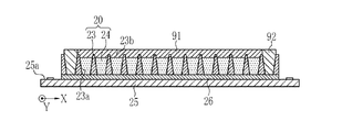
また、上記実施形態では、各開口部23aの空隙23bのみを埋めるように樹脂層27を形成しているが、図10に示すように、蛍光体支持基板25の表面25aからの高さが蛍光体層20より高い壁部90を、蛍光体層20の外周を囲うように形成し、壁部90で囲われた蛍光体層20上の空間(空隙23bを含む)を埋めるように、樹脂層91を形成してもよい。これにより、樹脂層91の表面の平坦性が向上する。
Moreover, in the said embodiment, although the
この場合、樹脂層91の表面上に粘着層29を形成し、蛍光体層20を、樹脂層91及び粘着層29を介して光電変換パネル21に貼り合わせてもよいが、粘着層29を設けず、樹脂層91の表面を光電変換パネル21に直接接触させてもよい。このように粘着層29を設けない場合には、蛍光体支持基板25と光電変換パネル21との間に、前述の端部封止部を設けることが好ましい。
In this case, the
また、図11に示すように、隔壁23の開口部23aのうち、最も外側に位置する開口部23aに樹脂を充填することにより、蛍光体層20の外周を囲う壁部92を形成し、壁部92で囲われた蛍光体層20上の空間(空隙23bを含む)を埋めるように、前述の樹脂層91を形成してもよい。この場合も同様に、樹脂層91の表面上に粘着層29を形成してもよいし、粘着層29を形成せずに、樹脂層91を光電変換パネル21に直接当接させてもよい。
Moreover, as shown in FIG. 11, the
また、図14に示すように、熱により塑性変形するシート状の樹脂層93を蛍光体層20の表面に押し当て、熱を加えて樹脂層93を変形させることにより、樹脂層93の一部で空隙23bを埋めてもよい。この場合も同様に、樹脂層93の表面上に粘着層29を形成してもよいし、粘着層29を形成せずに、樹脂層93を光電変換パネル21に直接当接させてもよい。樹脂層93の屈折率は、蛍光体24の屈折率に近いことが好ましい。
Further, as shown in FIG. 14, a part of the
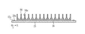
また、上記実施形態では、XY面に平行な方向における開口部23aの断面積が光電変換パネル21から離れる方向に単調に減少する隔壁23を用いているが、開口部の断面積が、光電変換パネル21側のほうが、光電変換パネル21とは反対側より大きければ(X線入射側の開口率が、X線入射側とは反対側の開口率大きければ)、どのような隔壁を用いてもよい。例えば、図13に示すように、開口部94aの断面積が階段状に変化する隔壁94を用いてもよい。また、図14に示すように、開口部95aの断面積が光電変換パネル21側から離れる方向に所定の位置まで単調に減少し、所定の位置から階段状に変化して一定となる隔壁95を用いてもよい。
Moreover, in the said embodiment, although the cross-sectional area of the
また、上記実施形態では、隔壁23の蛍光体支持基板25からの高さが一定であるが、これに代えて、X方向に平行な部分とY方向に平行な部分とで、蛍光体支持基板25からの高さが異なる隔壁を用いてもよい。このような隔壁は、プラズマディスプレイパネル用部材として特開2009−231280号公報により知られている。
Moreover, in the said embodiment, although the height from the fluorescent
また、上記実施形態では、隔壁23を、感光性ペーストを用いてフォトリソグラフィ(感光性ペースト法)により形成しているが、特開2009−231280号公報に記載されているように、サンドブラスト法やスクリーン印刷法を用いて形成することも可能である。また、隔壁23は、ガラスペーストに限られず、レジスト材等の他の材料で形成してもよい。さらに、隔壁23の側面に、金属等で反射膜を形成してもよい。
In the above embodiment, the
また、上記実施形態では、図3に示すように正方格子状の隔壁23を用いているが、X方向またはY方向に平行な溝を有するストライプ状の隔壁を用いてもよい。正方格子状の隔壁23の場合には、複数の孤立した開口部23aを有するため、蛍光体塗布液を充填する際に、塗布ムラが生じると、蛍光体塗布液が十分に充填されない開口部23aが生じるが、ストライプ状の隔壁の場合には、蛍光体塗布液を塗布する際に各溝に蛍光体塗布液が流動して一様に満たされるため、充填不良が生じにくいという利点がある。
In the above embodiment, the square lattice-
また、上記実施形態では、蛍光体粒子24bとしてGOS粒子を用いているが、蛍光体粒子24bとして、A2O2S:X(ただし、Aは、Y,La,Gd,Luのうちいずれか1つ、Xは、Eu,Tb,Prのうちのいずれか1つ)で表される粒子を用いることが可能である。また、蛍光体粒子24bとして、A2O2S:Xに共付活剤としてセリウム(Ce)またはサマリウム(Sm)を含めたものを用いてもよい。
In the above embodiment, GOS particles are used as the
また、上記実施形態では、TFT42の活性層42aをアモルファスシリコンにより形成しているが、これに代えて、非晶質酸化物(例えば、In−O系)、有機半導体材料、カーボンナノチューブなどにより形成してもよい。
In the above embodiment, the
また、上記実施形態では、PD43の半導体層43bをアモルファスシリコンにより形成しているが、これに代えて、有機光電変換材料(例えば、キナクリドン系有機化合物やフタロシアニン系有機化合物)により形成してもよい。アモルファスシリコンは、幅広い吸収スペクトルを持つが、有機光電変換材料は、可視域にシャープな吸収スペクトルを持つため、蛍光体層20で生成された可視光以外の電磁波を吸収することが殆どなく、ノイズを抑制することができる。
In the above embodiment, the
また、上記実施形態では、放射線としてX線を用いているが、γ線やα線等、X線以外の放射線を用いてもよい。さらに、上記実施形態では、可搬型の放射線画像検出装置である電子カセッテを例に挙げて本発明を説明しているが、本発明は、立位型や臥位型の放射線画像検出装置や、マンモグラフィ装置等にも適用可能である。 In the above embodiment, X-rays are used as radiation. However, radiation other than X-rays such as γ-rays and α-rays may be used. Furthermore, in the above embodiment, the present invention has been described by taking an electronic cassette as a portable radiological image detection device as an example, but the present invention is a standing radiograph or radiological image detection device, It can also be applied to a mammography apparatus.
10 X線画像検出装置
12 回路支持基板
20 蛍光体層
21 光電変換パネル
23 隔壁
23a 開口部
23b 空隙
24 蛍光体
24a バインダ
24b 蛍光体粒子
25 蛍光体支持基板
26 光反射膜
27 樹脂層
29 粘着層
41 画素
43 フォトダイオード
DESCRIPTION OF
Claims (10)
隔壁と蛍光体とを備え、前記隔壁は、前記各フォトダイオードに対応して配置されるとともに、前記撮像面に平行な方向の断面積が、前記光電変換パネル側のほうが、前記光電変換パネルとは反対側より大きい開口部を有し、前記蛍光体は、前記各開口部内に、前記光電変換パネル側に空隙を残して充填され、放射線を可視光に変換する蛍光体層と、
前記空隙に形成された樹脂層と、
を備えることを特徴とする放射線画像検出装置。 A photoelectric conversion panel having an imaging surface in which pixels including photodiodes that perform photoelectric conversion are two-dimensionally arranged;
A partition wall and a phosphor, and the partition wall is disposed corresponding to each of the photodiodes, and a cross-sectional area in a direction parallel to the imaging surface is closer to the photoelectric conversion panel than the photoelectric conversion panel side. Has a larger opening than the opposite side, the phosphor is filled in each opening, leaving a gap on the photoelectric conversion panel side, and a phosphor layer for converting radiation into visible light, and
A resin layer formed in the gap;
A radiological image detection apparatus comprising:
Priority Applications (1)
| Application Number | Priority Date | Filing Date | Title |
|---|---|---|---|
| JP2013056554A JP2014182002A (en) | 2013-03-19 | 2013-03-19 | Radiographic image detector |
Applications Claiming Priority (1)
| Application Number | Priority Date | Filing Date | Title |
|---|---|---|---|
| JP2013056554A JP2014182002A (en) | 2013-03-19 | 2013-03-19 | Radiographic image detector |
Publications (1)
| Publication Number | Publication Date |
|---|---|
| JP2014182002A true JP2014182002A (en) | 2014-09-29 |
Family
ID=51700853
Family Applications (1)
| Application Number | Title | Priority Date | Filing Date |
|---|---|---|---|
| JP2013056554A Pending JP2014182002A (en) | 2013-03-19 | 2013-03-19 | Radiographic image detector |
Country Status (1)
| Country | Link |
|---|---|
| JP (1) | JP2014182002A (en) |
Cited By (2)
| Publication number | Priority date | Publication date | Assignee | Title |
|---|---|---|---|---|
| WO2020036259A1 (en) * | 2018-08-13 | 2020-02-20 | 주식회사 이와이엘 | Method and apparatus for random number generation using inorganic scintillator |
| WO2022138657A1 (en) * | 2020-12-22 | 2022-06-30 | 富士フイルム株式会社 | Medical instrument |
-
2013
- 2013-03-19 JP JP2013056554A patent/JP2014182002A/en active Pending
Cited By (4)
| Publication number | Priority date | Publication date | Assignee | Title |
|---|---|---|---|---|
| WO2020036259A1 (en) * | 2018-08-13 | 2020-02-20 | 주식회사 이와이엘 | Method and apparatus for random number generation using inorganic scintillator |
| KR20200018935A (en) * | 2018-08-13 | 2020-02-21 | 주식회사 이와이엘 | Random number generation method and random number generator using inorganic scintillator |
| KR102093317B1 (en) | 2018-08-13 | 2020-03-25 | 주식회사 이와이엘 | Random number generation method and random number generator using inorganic scintillator |
| WO2022138657A1 (en) * | 2020-12-22 | 2022-06-30 | 富士フイルム株式会社 | Medical instrument |
Similar Documents
| Publication | Publication Date | Title |
|---|---|---|
| JP4921180B2 (en) | Radiation detection apparatus and radiation imaging system | |
| EP2902807B1 (en) | Radiograph detection device | |
| JP5693173B2 (en) | Radiation detection apparatus and radiation detection system | |
| US20020159563A1 (en) | Radiation imaging apparatus and radiation imaging system using the same | |
| JP5693174B2 (en) | Radiation detection apparatus and radiation detection system | |
| JP2001074847A (en) | Radiation image pickup device and radiation image pickup system | |
| JP5906162B2 (en) | Radiation image detection device | |
| US20130168559A1 (en) | Radiation detection apparatus | |
| JP2011149910A (en) | Radiation detector | |
| JP2005526961A (en) | X-ray image sensor | |
| WO2016111093A1 (en) | Radiation detector and manufacturing method therefor | |
| US9006662B2 (en) | Radiological image detection device | |
| JP2004317300A (en) | Plane radiation detector and its manufacturing method | |
| JP2014182002A (en) | Radiographic image detector | |
| JP2014182000A (en) | Radiographic image detector | |
| JP2014182001A (en) | Radiographic image detector | |
| JP2016136160A (en) | Radiographic image detection device | |
| JP2014066671A (en) | Radiation image detector | |
| WO2012165156A1 (en) | Radiation-image-capturing device | |
| JP7199332B2 (en) | Method for manufacturing radiation detection module | |
| CN111868567A (en) | Radiation detection panel, radiation detector, and method for manufacturing radiation detection panel | |
| JP2006186031A (en) | Photoelectric conversion device and radiation imager | |
| JP6953186B2 (en) | Radiation detector | |
| JP2024051180A (en) | Radiation imaging panel, radiation imaging device, radiation imaging system, method for manufacturing radiation imaging panel, and scintillator plate | |
| JP2024004725A (en) | radiation detector |