WO2012165156A1 - Radiation-image-capturing device - Google Patents
Radiation-image-capturing device Download PDFInfo
- Publication number
- WO2012165156A1 WO2012165156A1 PCT/JP2012/062624 JP2012062624W WO2012165156A1 WO 2012165156 A1 WO2012165156 A1 WO 2012165156A1 JP 2012062624 W JP2012062624 W JP 2012062624W WO 2012165156 A1 WO2012165156 A1 WO 2012165156A1
- Authority
- WO
- WIPO (PCT)
- Prior art keywords
- radiation
- absorbing
- scintillator
- image
- light
- Prior art date
Links
Images


Classifications
-
- G—PHYSICS
- G01—MEASURING; TESTING
- G01T—MEASUREMENT OF NUCLEAR OR X-RADIATION
- G01T1/00—Measuring X-radiation, gamma radiation, corpuscular radiation, or cosmic radiation
- G01T1/16—Measuring radiation intensity
- G01T1/20—Measuring radiation intensity with scintillation detectors
- G01T1/2018—Scintillation-photodiode combinations
- G01T1/20188—Auxiliary details, e.g. casings or cooling
- G01T1/20189—Damping or insulation against damage, e.g. caused by heat or pressure
-
- G—PHYSICS
- G01—MEASURING; TESTING
- G01T—MEASUREMENT OF NUCLEAR OR X-RADIATION
- G01T1/00—Measuring X-radiation, gamma radiation, corpuscular radiation, or cosmic radiation
- G01T1/16—Measuring radiation intensity
- G01T1/20—Measuring radiation intensity with scintillation detectors
- G01T1/2018—Scintillation-photodiode combinations
- G01T1/20188—Auxiliary details, e.g. casings or cooling
- G01T1/2019—Shielding against direct hits
-
- A—HUMAN NECESSITIES
- A61—MEDICAL OR VETERINARY SCIENCE; HYGIENE
- A61B—DIAGNOSIS; SURGERY; IDENTIFICATION
- A61B6/00—Apparatus for radiation diagnosis, e.g. combined with radiation therapy equipment
- A61B6/42—Apparatus for radiation diagnosis, e.g. combined with radiation therapy equipment with arrangements for detecting radiation specially adapted for radiation diagnosis
- A61B6/4283—Apparatus for radiation diagnosis, e.g. combined with radiation therapy equipment with arrangements for detecting radiation specially adapted for radiation diagnosis characterised by a detector unit being housed in a cassette
-
- A—HUMAN NECESSITIES
- A61—MEDICAL OR VETERINARY SCIENCE; HYGIENE
- A61B—DIAGNOSIS; SURGERY; IDENTIFICATION
- A61B6/00—Apparatus for radiation diagnosis, e.g. combined with radiation therapy equipment
- A61B6/42—Apparatus for radiation diagnosis, e.g. combined with radiation therapy equipment with arrangements for detecting radiation specially adapted for radiation diagnosis
- A61B6/4291—Apparatus for radiation diagnosis, e.g. combined with radiation therapy equipment with arrangements for detecting radiation specially adapted for radiation diagnosis the detector being combined with a grid or grating
-
- G—PHYSICS
- G03—PHOTOGRAPHY; CINEMATOGRAPHY; ANALOGOUS TECHNIQUES USING WAVES OTHER THAN OPTICAL WAVES; ELECTROGRAPHY; HOLOGRAPHY
- G03B—APPARATUS OR ARRANGEMENTS FOR TAKING PHOTOGRAPHS OR FOR PROJECTING OR VIEWING THEM; APPARATUS OR ARRANGEMENTS EMPLOYING ANALOGOUS TECHNIQUES USING WAVES OTHER THAN OPTICAL WAVES; ACCESSORIES THEREFOR
- G03B42/00—Obtaining records using waves other than optical waves; Visualisation of such records by using optical means
- G03B42/02—Obtaining records using waves other than optical waves; Visualisation of such records by using optical means using X-rays
- G03B42/04—Holders for X-ray films
Definitions
- the present invention relates to a radiation imaging apparatus for capturing a radiation image.
- the radiation imaging system for imaging a subject (a region to be imaged by a patient) using radiation (for example, X-rays) to perform image diagnosis.
- the radiation imaging system has a radiation generating device for emitting radiation and a radiation imaging device for capturing a radiation image of an imaging region.
- the radiation imaging apparatus includes a stationary type incorporated in a standing position imaging table or a reclining position imaging table, and a portable type that can be carried (so-called electronic cassette).
- a portable radiographic imaging device can be inserted under the patient sleeping on a bed in a hospital room or the like and imaged.
- an FPD flat panel detector
- the FPD detects a radiation image by accumulating signal charges for each pixel on the detection surface, and outputs this as digital image data.
- FPD a direct conversion type FPD that converts radiation directly into signal charge in a conversion layer made of amorphous selenium (a-Se) or the like, and an indirect conversion that converts radiation once into visible light and converts visible light into signal charge Type FPD is known.
- the indirect type FPD is composed of a scintillator that converts radiation into visible light, a detection panel disposed opposite to the scintillator, and an electrical control circuit.
- the detection panel has a detection surface in which a photoelectric conversion unit that generates a signal charge by photoelectric conversion is formed for each pixel, converts visible light from the scintillator into a signal charge, and stores the signal charge.
- a TFT panel in which TFTs (thin-film transistors) and photoelectric conversion parts are arranged in a matrix on a glass substrate, or a CMOS image sensor (hereinafter referred to as a CMOS sensor) is used.
- the TFT is formed of an amorphous semiconductor such as amorphous silicon (a-Si).
- a-Si amorphous silicon
- photoelectric conversion parts and MOS transistors are formed in a matrix on a single crystal semiconductor substrate of silicon (Si) by a semiconductor process.
- the MOS transistor of the CMOS sensor is formed of a single crystal semiconductor, its carrier mobility is three to four orders of magnitude higher than that of a TFT panel formed of an amorphous semiconductor, enabling high-speed readout of signal charges. is there.
- the variation of characteristics for example, the threshold voltage of the MOS transistor and the like
- the CMOS sensor is suitable for moving image shooting and high-quality shooting.
- CMOS sensors can now be manufactured using a 12 inch wafer, with one side of the square having a size of about 200 mm. Therefore, for example, an FPD having a size of 17 inches, which is generally used for medical use, can be configured using four CMOS sensors.
- the radiation image capturing apparatus is set under the patient A protective structure for preventing damage in the case is required, and the radiographic imaging device becomes large.
- Japanese Patent Application Laid-Open No. 2005-249639 a scattered X-ray absorbing grid for absorbing X-rays scattered by a subject is disposed between the subject and the radiation imaging apparatus, and the outer periphery of the scattered X-ray absorbing grid is disposed What provided the absorption part which absorbs the X-ray irradiated to the blank area is disclosed. Further, Japanese Patent Application Laid-Open No. 2010-075553 discloses that a radiation generating apparatus is provided with a filter in which the amount of absorption of X-rays irradiated to the blank area is increased.
- both the absorbing unit described in JP-A-2005-249639 and the filter described in JP-A-2010-075553 absorb X-ray components necessary for imaging, and the image quality of the radiation image is degraded.
- neither JP-A-2005-249639 nor JP-A-2010-075553 describes the prevention of deterioration of the characteristics of the CMOS sensor and the prevention of damage.
- An object of the present invention is to provide a radiation image capturing apparatus capable of preventing characteristic deterioration of a radiation detector due to radiation and preventing damage due to a load or an impact from a subject.
- a radiation imaging device of the present invention is provided with a radiation detector and a radiation absorption part.
- the radiation detector detects radiation transmitted through the subject and generates image data.
- the radiation absorbing portion is disposed on the radiation incident side of the radiation detector, absorbs a part of the radiation incident on the radiation detector, and is deformable by the load of the subject.
- the radiation detector has a single crystal semiconductor substrate.
- the radiation absorbing portion has a bag and a liquid or gel radiation absorbing fluid sealed in the bag.
- a liquid scintillator that absorbs radiation and converts it into light may be used.
- a gelled water glass may be used as the radiation absorbing fluid.
- the radiation absorbing fluid may also have a liquid or gel fluid and a radiation absorbing material dispersed in the fluid.
- the radiation absorbing portion may have an elastic body which is deformed by a load from a subject, and a radiation absorbing material dispersed in the elastic body. Also, a plurality of radiation absorbing portions may be provided.
- the radiation detector has a scintillator that absorbs radiation and converts it into light, and a sensor panel that is disposed on the radiation irradiation side of the scintillator and that detects light converted by the scintillator.
- the radiation absorber preferably has a bag and a liquid scintillator enclosed in the bag.
- a signal output circuit includes a plurality of pixels including a photoelectric conversion layer that converts light converted by a scintillator into electric charge and a signal output circuit that outputs a signal according to the electric charge converted by the photoelectric conversion layer as a sensor panel Any of those provided over a single crystal semiconductor substrate can be used. As such a sensor panel, one configured by a CMOS type image sensor is used.
- the photoelectric conversion layer is preferably formed of amorphous silicon or quinacridone.
- the wavelength range of light generated by the liquid scintillator be different from the wavelength range of light detectable by the sensor panel.
- the radiation absorber is preferably larger in size than the radiation detector. It is preferable to include an image correction unit that corrects image data according to the area difference of the radiation absorption amount of the radiation absorption unit.
- the radiation absorbing portion preferably absorbs the low energy component of the radiation.
- the low energy component of the radiation absorbed by the radiation absorbing portion is an energy component of 1/2 or less of the energy distribution of the radiation.
- the radiation absorbing unit absorbs a part of the radiation, it is possible to suppress the characteristic deterioration of the radiation detector. Further, the radiation detector can be reinforced by the radiation absorbing portion to prevent damage to the radiation detector.
- the radiation absorbing portion is deformed by the load from the subject, the radiation absorption distribution is optimized according to the position, size, and range of the subject. As a result, the radiation transmitted through the subject does not deteriorate the image quality of the radiation image because the amount of radiation absorbed by the radiation absorbing portion is small, and the amount of radiation absorbed in the blank area directly irradiated with radiation is large, and the characteristics of the radiation detector deteriorate Is suppressed.
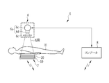
- a radiation imaging system 5 comprises: a radiation generator 6 for emitting X-rays as radiation toward the imaging region of a subject (patient) H; a radiation imaging apparatus 7 for imaging a radiation image of the subject H; A console 8 for controlling the radiation generator 6 and the radiation imaging device 7 is provided.
- the radiation generator 6 has a radiation source 6a and a source filter 6b.
- the radiation source 6a has an X-ray tube 6c for emitting X-rays and a radiation field limiter (collimator) 6d for limiting the radiation field of X-rays emitted by the X-ray tube 6c.
- the X-ray tube 6c has a cathode formed of a filament that emits thermoelectrons, and an anode (target) that emits thermorays which collide with the thermoelectrons emitted from the cathode.
- the irradiation field limiter 6d is, for example, a plurality of lead plates for shielding X-rays arranged on each side of a square and an irradiation opening for transmitting X-rays formed at the center, and the position of the lead plate is moved By changing the size of the irradiation opening, the irradiation field is limited.
- the radiation source filter 6b removes low energy components which are scattered when passing through the imaging region from the X-rays emitted from the radiation source 6a and cause deterioration of the radiation image.
- a material having a property of absorbing only the low energy component of the X-ray is used.
- aluminum is suitable.
- the high energy component of the X-ray transmitted through the radiation source filter 6 b is used for imaging the subject H.
- the energy distribution of the X-rays emitted from the X-ray tube 6c is, for example, approximately when the tube voltage of the X-ray tube 6c is 70 kV and the maximum energy of the X-rays emitted from the X-ray tube 6c is about 70 KeV 15 to 70 KeV.
- about 1/2 or less (15 to 40 KeV) of the energy distribution of the X-ray is a low energy component, and 1/2 or more (40 to 70 KeV) is a high energy component.
- the source filter 6b absorbs low energy components of 15 to 40 KeV.
- the radiation image capturing apparatus 7 includes an FPD 19, a radiation absorbing unit 20, a light absorbing layer 21, an electric circuit unit 23, and a portable case 12.
- the housing 12 has a top plate 13 and a flat box-shaped housing body 14, and accommodates the FPD 19 and the electric circuit unit 23.
- the top plate 13 seals the opening 14 a at the top of the case body 14.
- the upper surface of the top plate 13 is an irradiation surface 11 to which X-rays emitted from the radiation generator 6 are irradiated.
- the top plate 13 is formed of carbon or the like having high X-ray permeability. Since carbon has high strength, it is suitable as a material of the top 13 to which the weight of the subject H is applied.
- the housing body 14 is formed of ABS resin or the like.
- the housing 12 is the same size (e.g., 17 inches by 17 inches) as a conventional radiation film cassette for recording a radiation image on a photosensitive material.
- the radiographic imaging device 7 has the same portability as the radiographic film cassette, and is used in place of the radiographic film cassette.
- the top plate 13 is provided with a display unit 16 configured of a plurality of LEDs.
- the display unit 16 displays an operation mode (e.g., "ready state” or “during data transmission” or the like) of the radiation imaging device 7 and an operation state such as a remaining capacity of a battery.
- the display unit 16 may be configured by a light emitting element other than an LED, a liquid crystal display, an organic EL display, or the like.
- the display unit 16 may be provided in the housing body 14.
- the light absorbing layer 21 and the radiation absorbing portion 20 are stacked in this order on the top plate 13.
- the radiation absorbing unit 20 faces the top 13 via the light absorbing layer 21.
- the radiation absorbing unit 20 absorbs a part of X-rays (for example, low energy components of X-rays) irradiated to the irradiation surface 11 and protects the FPD 19 from a load, an impact or the like applied to the top plate 13.
- the light absorbing layer 21 absorbs the light generated by the radiation absorbing unit 20 by the X-ray irradiation.
- the electric circuit unit 23 accommodates a signal processing unit 50, an image memory 51, a control unit 52, a wireless communication unit 53, a battery 54 and the like (all refer to FIG. 9).
- the electric circuit unit 23 is disposed at one end side along the short direction inside the housing 12.
- the FPD 19 operates by the power supplied from the battery 54.
- a radiation shielding member (not shown) such as a lead plate is provided on the top plate 13 side of the electric circuit section 23 in order to prevent the electric circuit section 23 from being damaged by X-rays.
- a light absorbing layer 21 is attached to the top surface of the top plate 13 with an adhesive (not shown).
- the radiation absorbing portion 20 is attached onto the light absorbing layer 21 by an adhesive (not shown).
- the light absorbing layer 21 and the radiation absorbing unit 20 cover the irradiation surface 11. Thereby, the radiation imaging device 7 can be thinned and the radiation detector 19 can be reinforced.
- the FPD 19 is one in which a sensor panel 25 and a scintillator 26 are sequentially stacked from the top 13 side along the direction in which the radiation is irradiated.
- a support substrate 27 supporting the scintillator 2 is provided on the lower surface of the scintillator 26.
- a sealing agent 28 is provided on the outer periphery of the FPD 19 in order to protect the scintillator 26 from moisture and the like.
- a drive circuit board 29 of the FPD 19 is disposed on the bottom of the housing 12. The drive circuit board 29 and the sensor panel 25 are electrically connected via the flexible cable 30.
- the scintillator 26 transmits the subject H and is irradiated to the irradiation surface 11 of the housing 12, and transmits the top plate 13, the radiation absorbing unit 20, and the sensor panel 25 to absorb incident X-rays and generate visible light.
- CsI: Tl cesium iodide to which thallium is added
- CsI: Na cesium iodide to which sodium is added
- GOS Gd 2 O 2 S: Tb
- CsI: Tl is used as the scintillator 26.
- the scintillator 26 is formed by vapor deposition of CsI: Tl on the support substrate 27.
- the scintillator 26 has a columnar crystal structure, and has a plurality of columnar crystals (not shown) along the direction from the support substrate 27 toward the sensor panel 25.
- the columnar crystal has a flat diameter substantially uniform along the longitudinal direction of the columnar crystal.
- the light generated by the scintillator 26 propagates in the columnar crystal due to the light guide effect of the columnar crystal, and is emitted toward the sensor panel 25 from the tip of the columnar crystal.
- the scintillator 26 in a columnar crystal structure, diffusion of visible light emitted from the scintillator 26 to the sensor panel 25 side is suppressed, so the sharpness of the radiation image captured by the radiation imaging device 7 Improve.
- a reflective layer (not shown) is provided on the surface of the support substrate 27 on the scintillator 26 side.
- the visible light emitted by the scintillator 26 and propagated to the support substrate 27 is reflected to the sensor panel 25 by the reflective layer, so the amount of light incident on the sensor panel 25 (detection efficiency of light emitted by the scintillator 26) is improved. Do.
- the configuration in which the sensor panel 25 is disposed on the X-ray incident side of the scintillator 26 is referred to as an ISS (Irradiation Side Sampling) method.
- a configuration in which the sensor panel is disposed on the opposite side to the X-ray incident side of the scintillator is called a PSS (Penetration Side Sampling) method.
- PSS Pulsion Side Sampling
- the sharpness and sensitivity of the radiation image are improved compared to the PSS method.
- the sensor panel 25 is configured by four CMOS type image sensors (hereinafter referred to as CMOS sensors) 33.
- CMOS sensors CMOS type image sensors
- Each CMOS sensor 33 has a plurality of pixels 33a (see FIG. 7) arranged in a matrix.
- Each CMOS sensor 33 has a rectangular shape with a side length of about 200 mm.
- the four CMOS sensors 33 are arranged adjacent to each other vertically and horizontally, and form a square of approximately 17 inches on a side.
- the CMOS sensor 33 has a configuration similar to that disclosed in U.S. Patent Publication 2009/0224162. Specifically, as shown in FIG. 5, the CMOS sensor 33 is constituted of a single crystal semiconductor substrate 34, an insulating layer 35, a first electrode 36, a photoelectric conversion layer 37, and a second electrode 38. There is.
- the single crystal semiconductor substrate 34 is made of single crystal Si.
- the insulating layer 35 is formed on the surface of the single crystal semiconductor substrate 34, and silicon oxide or the like is used for the insulating layer 35.
- the first electrode 36 is individually formed for each pixel 33 a on the surface of the insulating layer 35.
- the photoelectric conversion layer 37 is provided on the surface of each first electrode 36 in common to each pixel 33 a.
- the second electrode 38 is provided on the surface of the photoelectric conversion layer 37 in common to each pixel 33 a.
- the aforementioned scintillator 26 is bonded onto the surface of the second electrode 38 by an adhesive (not shown).
- the second electrode 38 is formed of a conductive material (for example, indium tin oxide (ITO)) which is transparent to visible light so that visible light generated by the scintillator 26 is incident on the photoelectric conversion layer 37.
- ITO indium tin oxide
- the second electrode 38 is provided in common to each pixel 33a, but may be provided individually for each pixel 33a.
- the photoelectric conversion layer 37 generates a signal charge according to the amount of incident X-rays, in combination with the scintillator 26.
- the photoelectric conversion layer 37 absorbs visible light generated by the scintillator 26, generates a signal charge according to the amount of absorbed light, and is formed of an organic or inorganic photoelectric conversion material.
- the inorganic photoelectric conversion material include amorphous silicon (a-Si).
- An example of the organic photoelectric conversion material is quinacridone.
- the sensitivity of the organic photoelectric conversion material (OPC) made of quinacridone is closer to the wavelength range of visible light generated by CsI: Tl than by CsI: Na or single crystal Si (c-Si). .
- CsI: Tl as the scintillator 26
- a signal output circuit 41 is provided for each pixel 33a.
- the signal output circuit 41 is formed of a CMOS circuit.
- the signal output circuit 41 and the first electrode 36 are electrically connected by the contact wiring 42.
- a bias voltage is applied to the second electrode 38 (see FIG. 7), and the signal charge generated by the photoelectric conversion layer 37 is collected by the first electrode 36 of each pixel 33 a.
- the signal output circuit 41 converts the signal charge collected by the first electrode 36 into a voltage signal corresponding to the signal charge amount and outputs the voltage signal.
- the signal output circuit 41 includes an output transistor T1, a row selection transistor T2, a reset transistor T3, a row selection line L1, a signal output line L2, and a reset line L3.
- the output transistor T1, the row selection transistor T2, and the reset transistor T3 are each a MOS transistor.
- the row selection line L1, the signal output line L2, and the reset line L3 are formed of a metal such as aluminum in the insulating layer 35 described above.
- the output transistor T1 is connected to the first electrode 36, and a voltage corresponding to the signal charge collected by the first electrode 36 is applied to the gate.
- the row selection transistor T2 is turned on by the selection signal applied to the row selection line L1, and a voltage signal controlled according to the gate voltage of the output transistor T1 is applied to the signal output line L2.
- the reset transistor T3 is turned on by the selection signal applied to the reset line L3, and discards the signal charge collected by the first electrode 36 to the power supply wiring Vdd.
- the carrier mobility of each of the transistors T1 to T3 is higher than that of a TFT made of an amorphous semiconductor such as a-Si.
- a control unit of the FPD 19 can be mixedly mounted on the single crystal semiconductor substrate 34.
- the row selection line L1, the signal output line L2, and the reset line L3 are formed of a metal such as aluminum, so there is little deterioration due to X-rays, but the output transistor T1, the row selection transistor T2, the reset Since the transistor T3 is formed of single crystal Si, there is a possibility that the characteristics may be degraded (change in threshold voltage or increase in dark current) due to X-rays. This is because in the MOS structure using single crystal Si, charges (hereinafter referred to as interface charge) are generated and accumulated at the interface between the single crystal semiconductor substrate 34 and the insulating layer 35 by absorption of X-rays.
- interface charge charges
- the radiation absorbing portion 20 absorbs a part of the X-rays transmitted through the top plate 13 (a low energy component affecting the characteristic deterioration of the MOS transistor).
- the high energy component of the X-ray passes through the CMOS sensor 33, but the low energy component of the X-ray does not have enough energy to pass through the CMOS sensor 33, and is absorbed by the CMOS sensor 33.
- the radiation absorbing portion 20 is composed of a bag 47 and a radiation absorbing fluid 48.
- the bag body 47 has elasticity that can be deformed by the load of the subject H.
- the radiation absorbing fluid 48 is enclosed in a bag 47.
- the bag body 47 is formed in a bag shape, for example, of an elastic material such as rubber or plastic material having a thickness of about several mm to 1 cm.
- the radiation absorbing fluid 48 is liquid or gel and has a property of absorbing a part of X-rays (low energy component). In the present embodiment, a liquid scintillator that absorbs X-rays and converts them into light is used as the radiation absorbing fluid 48.
- the liquid scintillator is formed of a solute composed of a phosphor, a solvent in which the solute is mixed, a surfactant, and the like.
- the properties of the liquid scintillator depend on the type and amount of solvent, solute, surfactant and the like.
- mixed xylene (isomer), toluene, pseudocumene, dioxane or the like is used as the solvent.
- solute for example, PPO, bulty-PBD, DMPOPOP, Bis-MSB or the like is used.
- the solution mass is, for example, 0.5 to 5 g / liter to construct a liquid scintillator.
- PPO is used as a solute, an emission spectrum of 440 nm or less is obtained. It is also possible to shift the emission spectrum to the long wave side by mixing a wavelength conversion material in the solute.
- the light absorbing layer 21 absorbs the light converted from the X-rays by the radiation absorbing unit 20 to prevent the light of the radiation absorbing unit 20 from being incident on the sensor panel 25. This prevents the image quality of the radiation image.
- the light absorption layer 21 is formed of a material capable of absorbing light emitted by the liquid scintillator.
- the imaging region of the subject H when the imaging region of the subject H is a hand, the imaging region is smaller than the imaging range of the FPD 19. Moreover, in such a case, the imaging region is mostly imaged in a state of being disposed at the center of the imaging range of the FPD 19. For this reason, the peripheral portion other than the central portion where the imaging region is arranged becomes a blank area where the X-rays are directly irradiated to the FPD 19, and characteristic deterioration easily occurs in the CMOS sensor 33.
- the X-ray incident on the FPD 19 has a small amount of X-ray absorption by the radiation absorbing portion 20 in the central portion that affects the image quality of the radiation image, and in the peripheral portion corresponding to one missing region Preferably, the amount of absorption is large.
- the radiation absorbing unit 20 can be deformed by the weight of the subject H. Specifically, as shown in FIG. 9, when the subject H is placed at the central portion of the radiation absorbing unit 20, the bag 47 is deformed by its weight, and the radiation absorbing fluid 48 is a bag. It flows in the bag 47 in accordance with the deformation of the body 47. As a result, in the radiation absorbing unit 20, the thickness of the central portion immediately below the subject H is reduced, and the thickness of the peripheral portion is increased.
- the X-ray intensity I after passing through the object is represented by the following equation (1), and decreases exponentially as the thickness T of the object increases when the attenuation coefficient ⁇ is constant. Therefore, when the radiation absorbing portion 20 is deformed as shown in FIG. 9, the X-ray absorption amount at the peripheral portion becomes high, so that the characteristic deterioration of the CMOS sensor 33 in the blank area is suppressed. Further, the amount of absorption of X-rays at the central portion of the radiation absorbing portion 20 is reduced, and the subject H is in a state of being close to the top 13, so X-ray scattering by the radiation absorbing portion 20 hardly occurs. Image quality deterioration is suppressed.
- I I'exp (- ⁇ T) (1)
- I X-ray intensity after transmission
- I ' X-ray intensity before transmission
- ⁇ Attenuation coefficient (different according to the type of substance and density)
- T Transmission thickness
- the single crystal semiconductor substrate 34 of the CMOS sensor 33 is easily broken in material and thin as about several tens of ⁇ m, it is preferable that the single crystal semiconductor substrate 34 have a protective structure that prevents damage due to the load of the object H applied to the top plate 13 .
- the sensor panel 25 configured of four CMOS sensors 33, when an impact or load is applied to the central portion of the sensor panel 25, all four CMOS sensors 33 may be damaged, and the repair cost is very high. large.
- the radiation absorbing portion 20 is deformed by the load from the subject H to absorb the load and the impact applied to the central portion of the top 13, so that the CMOS sensor 33 can be prevented from being damaged.
- the radiation absorbing unit 20 can suppress the heat of the subject H from being transmitted to the sensor panel 25, and can also suppress the image quality deterioration of the radiation image due to the temperature unevenness of the sensor panel 25.
- the electric circuit of the radiation image capturing apparatus 7 includes a sensor panel 25, a signal processing unit 50, an image memory 51, a control unit 52, a wireless communication unit 53, a battery 54 and the like.
- the signal processing unit 50 includes an amplifier for amplifying a pixel signal output from each pixel 33 a of the sensor panel 25, an A / D (analog / digital) converter, and the like, and the pixel signal output from the sensor panel 25 Into digital image data.
- the signal processing unit 50 further includes an image correction unit 50 a that corrects a radiation image according to the absorption distribution of low energy components of X-rays by the radiation absorption unit 20. Since the region to be imaged is mostly placed at the central portion, the central portion of the radiation absorbing unit 20 becomes thinner at the time of imaging, and the X absorption amount is smaller than that at the peripheral portion. The state of depression at the center depends on the imaging site. Therefore, the thickness of each part with respect to the imaging site is determined experimentally. Then, a correction coefficient for obtaining an X-ray absorption amount for each pixel or area corresponding to the thickness amount is set in the image correction unit 50a.
- the image correction unit 50a corrects the image data using the correction coefficient by designating the imaging region with the console 8, thereby removing the influence of the X-ray absorption amount of the radiation absorption unit 20.
- the accuracy of the correction can be improved by inputting the gender or the weight and the height.
- An image memory 51 is connected to the signal processing unit 50, and the image data output from the image correction unit 50 a of the signal processing unit 50 is stored in the image memory 51.
- the image memory 51 has a storage capacity capable of storing image data of a plurality of frames. Image data obtained by imaging is sequentially stored in the image memory 51 each time a radiographic image is captured.
- the control unit 52 includes a CPU 52a, a RAM 52b, and a ROM 52, and controls the overall operation of the radiation imaging device 7.
- the RAM 52 b is a temporary storage memory made of a DRAM or the like.
- the ROM 52 is a non-volatile memory including a flash memory or the like.
- the wireless communication unit 53 is an IEEE (Institute of Electrical and Electronics). Engineers) correspond to wireless LAN (Local Area Network) standards represented by 802.11a / b / g / n etc., and enable wireless communication of various information with external devices.
- the control unit 52 performs wireless communication with the console 8 via the wireless communication unit 53, and transmits and receives various types of information to and from the console 8.
- the battery 54 supplies power to each part in the radiation imaging device 7.
- the battery 54 is a rechargeable secondary battery, and is detachable from the radiation imaging device 7.
- the signal processing unit 50, the image memory 51, the control unit 52, and the wireless communication unit 53 may be provided in the drive circuit board 29. These are connected to one another via a bus.
- the console 8 includes a CPU 57, a ROM 58, a RAM 59, and an HDD 60, which are connected to one another via a bus 67.
- the CPU 57 controls each part of the console 8.
- the ROM 58 stores various programs including a control program.
- the RAM 59 temporarily stores various data.
- the HDD 60 stores various data.
- a communication I / F 61, a wireless communication unit 62, a display driver 64, and an operation input detection unit 66 are connected to the bus 67.
- a display 63 is connected to the display driver 64.
- An operation panel 65 is connected to the operation input detection unit 66.
- the communication I / F 61 is connected to the communication I / F 70 of the radiation generation device 6 via the connection terminal 61 a, the communication cable 69, and the connection terminal 70 a of the radiation generation device 6.
- the CPU 57 of the console 8 performs transmission and reception of various information such as the irradiation condition with the radiation generator 6 via the communication I / F 61.
- the wireless communication unit 62 has a function of performing wireless communication with the wireless communication unit 53 of the radiation image capturing apparatus 7.
- the CPU 57 of the console 8 exchanges various information such as image data with the radiation imaging device 7 via the wireless communication unit 62.
- the display driver 64 generates and outputs a signal for displaying various information on the display 63.
- the CPU 57 of the console 8 causes the display 63 to display the operation menu, the captured radiographic image, and the like via the display driver 64.
- the operation panel 65 has a plurality of keys, and can input various information and operation instructions.
- the operation input detection unit 66 detects an operation performed on the operation panel 65, and transmits the detection result to the CPU 57.
- the radiation generating apparatus 6 is configured of a communication I / F 70, a radiation source control unit 72, and a radiation source 6a.
- the communication I / F 70 transmits and receives various information such as an irradiation condition to and from the console 8.
- the radiation source control unit 72 controls the radiation source 6 a based on the irradiation conditions (including the information of the tube voltage and the tube current) received from the console 8.
- the photographer inserts the radiation imaging device 7 between the imaging region of the subject H and the imaging table with the irradiation surface 11 facing the imaging region.
- the orientation, position, and the like of the radiation imaging device 7 are finely adjusted.
- the radiation imaging device 7 when the imaging region is directly placed on the radiation imaging device 7, the radiation imaging device 7 is subjected to an impact or a load when mounting the imaging region.
- the impact and load are absorbed by deformation of the radiation absorbing portion 20.
- the radiation image capturing apparatus 7 of the present embodiment is an ISS method, and the sensor panel 25 is disposed on the top plate 13 side of the scintillator 26, so that breakage of the sensor panel 25 is effectively prevented.
- the photographer When the preparation work is completed, the photographer operates the operation panel 65 to instruct start of imaging.
- the console 8 transmits an instruction signal instructing the start of exposure to the radiation generator 6, and the radiation generator 6 causes the radiation source 6a to emit X-rays.
- the low energy component is absorbed by the radiation source filter 6b, the X-ray emitted from the radiation source 6a is transmitted through the imaging region of the subject H, and is irradiated to the irradiation surface 11 through the radiation absorbing portion 20 and the light absorbing layer 21. Ru.
- the X-rays pass through the top plate 13 and the sensor panel 25 and enter the scintillator 26.
- the low energy component of the X-rays transmitted through the object H is absorbed by the radiation absorbing unit 20, so that the characteristic deterioration of each CMOS sensor 33 due to the sensor panel 25 absorbing the X-rays is suppressed.
- the radiation absorbing portion 20 is deformed by the weight of the object H, and the thickness of the peripheral portion is thicker than that of the central portion. Therefore, the characteristic deterioration due to direct irradiation of the X-ray to the peripheral portion Is effectively suppressed.
- the radiation absorbing portion 20 has a central portion thinner than the peripheral portion, X-rays transmitted through the imaging region of the subject H are not absorbed more than necessary, and the image quality of the radiation image is greatly degraded. There is no.
- the X-rays incident on the scintillator 26 are converted into visible light in the vicinity of the X-ray incident surface of the scintillator 26, that is, on the sensor panel 25 side.
- the visible light generated by the scintillator 26 the visible light propagating toward the sensor panel 25 is incident on the sensor panel 25.
- the visible light propagated toward the support substrate 27 is reflected by the reflective layer of the support substrate 27 and then passes through the scintillator 26 again toward the sensor panel 25, and the sensor The light is incident on the panel 25. Since the visible light emitted by the scintillator 26 is guided by the columnar crystal made of CsI: Tl, image blurring is suppressed.
- the visible light incident on the scintillator 26 is transmitted through the second electrode 38 and incident on the photoelectric conversion layer 37, and is converted into signal charge by the photoelectric conversion layer 37.
- the signal charge generated in the photoelectric conversion layer 37 is collected by the first electrode 36 and converted to a voltage signal by the signal output circuit 41 after the end of the X-ray emission.
- This voltage signal is sequentially output from each pixel 33a as a pixel signal.
- the output pixel signals are converted into image data by the signal processing unit 50.
- the image data is corrected by the image correction unit 50a according to the amount of X-ray absorption which changes with the thickness of each portion of the radiation absorption unit 20.
- the image data after correction is stored in the image memory 51.
- the CPU 52 a transmits the image data stored in the image memory 51 to the console 8 via the wireless communication unit 53.
- the CPU 57 of the console 8 stores the image data received from the radiation imaging device 7 in the HDD 60 via the RAM 59. Further, the CPU 57 causes the display 63 to display a radiation image based on the image data stored in the HDD 60 via the display driver 64.
- the characteristic deterioration of the CMOS sensor 33 is suppressed.
- the radiation absorbing unit 20 is deformed according to the position of the subject H placed on the radiation imaging device 7, and the amount of absorption of the low energy component changes, so that the image quality of the radiation image is not deteriorated. Characteristic deterioration of the CMOS sensor 33 in the missing region is suppressed.
- the conventional ISS-type radiation imaging apparatus using a TFT panel is not easy to apply to mammography with a low tube voltage because the X-ray absorption of alkali-free glass used as a substrate of the TFT panel is large.
- a CMOS sensor with low X-ray absorption can be used for a radiation imaging apparatus of ISS method, application to mammography is easy.
- the light absorbing layer 21 is separately provided to absorb the light emitted from the radiation absorbing unit 20, but the light is applied to the bonding surface of the bag 47 with the top plate 13 or the entire bag 47. It may have absorbency.
- the wavelength range of the light emitted from the radiation absorbing fluid 48 may be different from the wavelength range detectable by the sensor panel 25 by appropriately selecting the type of solute or the wavelength conversion material. Thereby, the light absorption layer 21 can be omitted.
- a liquid scintillator is used as the radiation absorbing fluid 48, but a paraffin scintillator may be used.
- the paraffin scintillator is waxy at low temperature and has fluidity at about 40 ° C.
- the paraffin scintillator is described in detail in Japanese Patent Application Laid-Open No. 07-301676, so the detailed description is omitted.
- gelled water glass sodium silicate
- the gelation of water glass occurs, for example, by adding an acid to water glass and stirring.
- the radiation absorbing fluid 48 may be configured by dispersing an X-ray absorbing material in a liquid or gel fluid.
- an X-ray absorbing material metals of atomic numbers 20 to 31 (for example, copper) having a high effect of absorbing low energy components of X-rays and little back scattering are preferable.
- the radiation absorption part 20 is comprised with the bag body 47 and the radiation absorptive fluid body 48, you may form with elastic bodies, such as rubber
- the one radiation absorption part 20 is provided in the radiographic imaging apparatus 7, you may provide several radiation absorption parts.
- a plate-like low energy absorbing plate 75 for absorbing low energy components of X-rays is disposed between the top plate 13 and the sensor panel 25.
- the low energy absorbing plate 75 may be disposed between the top plate 13 and the radiation absorbing unit 20, or the low energy absorbing plate 75 may be used instead of the top plate 13.
- the low energy absorbing plate 75 for example, aluminum, glass or the like can be used, but the same material as the above-mentioned source filter 6b may be included.
- the transmitted X-ray energy distribution becomes the same.
- X-rays that can pass through the radiation source filter 6b are difficult to be absorbed by the radiation absorbing unit 20 as well, so that it is possible to suppress X-rays including information of the object H from being absorbed by the radiation absorbing unit 20. As a result, the utilization efficiency of X-rays is improved.
- the CMOS sensor may be configured by an organic thin film transistor formed on a plastic film so as to impart flexibility to the CMOS sensor.
- organic thin film transistors see “Tsuyoshi Sekitani, Flexible organic”. Since this is described in detail in “Transistors and circuits with extreme bending stability, Nature Materials 9, November 7, 2010, pp. 1015-1022”, the detailed description will be omitted.
- a photodiode and a transistor formed of single crystal Si may be provided over a flexible plastic substrate.
- a device block of about several tens of microns in size is dispersed in a solution, and FAS (Fluidic Self- Assembly) can be used.
- FSA Fluidic Self- Assembly
- “Koichi Maezawa” Resonant tunnel device block fabrication technology for Fluidic Self-Assembly ", Technical Report of IEICE, ED, Electronic Device, The Institute of Electronics, Information and Communication Engineers, 2008 6 May 6, 108, 87, p. Detailed description will be omitted as it is described in detail in 67-71.
- the sensor panel is constituted by a CMOS sensor, but the present invention is also applicable to a radiation image photographing apparatus in which the sensor panel is constituted by a CCD image sensor formed by a single crystal semiconductor substrate. .
- the present invention is not limited to the ISS method, and is also applicable to a PSS type radiation imaging apparatus.
- the present invention is also applicable to a direct conversion type radiation imaging apparatus that converts radiation directly into electric charges.
- the FPD is incorporated into a cassette-sized casing
- a standing-type or lying-down type imaging device or a mammography device it is also possible to be incorporated into a standing-type or lying-down type imaging device or a mammography device.
- the present invention is also applicable to a radiation imaging apparatus using radiation other than X-rays, such as ⁇ -rays.
- the configuration of the radiation image capturing apparatus according to the present invention described in the above embodiment is an example, and it goes without saying that the configuration can be appropriately changed without departing from the scope of the present invention.
Abstract
A radiation-image-capturing device (7) has a sensor panel (25) made of a plurality of CMOS sensors (33). The sensor panel (25) has a signal-outputting circuit formed on a monocrystal semiconductor substrate. The top surface of a top plate (13) irradiated by x-rays is provided with a radiation-absorbing unit (20) for absorbing some of the x-rays (low-energy components) responsible for characteristics degradation of the signal-outputting circuit. The radiation-absorbing unit (20) is made of a bag (47) and a radiation-absorbing fluid (48) accommodated within the bag (47). The radiation-absorbing unit (20) is deformed under loading from a subject (H).
Description
本発明は、放射線画像を撮影する放射線画像撮影装置に関する。
The present invention relates to a radiation imaging apparatus for capturing a radiation image.
医療分野において、画像診断を行うために、放射線(例えば、X線)を利用して被写体(患者の撮影部位)を撮影する放射線撮影システムが知られている。放射線撮影システムは、放射線を照射する放射線発生装置と、撮影部位の放射線画像を撮影する放射線画像撮影装置とを有する。放射線画像撮影装置には、立位撮影台や臥位撮影台に組み込まれた据え置き型のものや、持ち運び可能な可搬型のもの(いわゆる電子カセッテ)がある。可搬型の放射線画像撮影装置は、病室等でベッドに寝ている患者の下に挿入して撮影することができる。
2. Description of the Related Art In the medical field, there is known a radiation imaging system for imaging a subject (a region to be imaged by a patient) using radiation (for example, X-rays) to perform image diagnosis. The radiation imaging system has a radiation generating device for emitting radiation and a radiation imaging device for capturing a radiation image of an imaging region. The radiation imaging apparatus includes a stationary type incorporated in a standing position imaging table or a reclining position imaging table, and a portable type that can be carried (so-called electronic cassette). A portable radiographic imaging device can be inserted under the patient sleeping on a bed in a hospital room or the like and imaged.
放射線画像撮影装置には、放射線の入射量に応じた信号電荷を蓄積する画素がマトリクス状に配列された検出面を有するFPD(flat panel detector)を放射線検出器として用いたものが実用化されている。FPDでは、検出面において画素毎に信号電荷を蓄積することで、放射線画像を検出し、これをデジタルの画像データとして出力する。
As a radiation imaging apparatus, one using an FPD (flat panel detector) having a detection surface in which pixels accumulating signal charges according to the amount of incident radiation are arranged in a matrix as a radiation detector is put to practical use. There is. The FPD detects a radiation image by accumulating signal charges for each pixel on the detection surface, and outputs this as digital image data.
FPDには、アモルファスセレン(a-Se)等からなる変換層で放射線を直接信号電荷に変換する直接変換型FPDと、放射線を一旦可視光に変換し、可視光を信号電荷に変換する間接変換型FPDが知られている。間接型FPDは、放射線を可視光に変換するシンチレータと、このシンチレータに対向して配置された検出パネルと、電気制御回路とで構成されている。検出パネルは、光電変換により信号電荷を発生する光電変換部を画素ごとに形成した検出面を有しており、シンチレータからの可視光を信号電荷に変換して蓄積する。
In FPD, a direct conversion type FPD that converts radiation directly into signal charge in a conversion layer made of amorphous selenium (a-Se) or the like, and an indirect conversion that converts radiation once into visible light and converts visible light into signal charge Type FPD is known. The indirect type FPD is composed of a scintillator that converts radiation into visible light, a detection panel disposed opposite to the scintillator, and an electrical control circuit. The detection panel has a detection surface in which a photoelectric conversion unit that generates a signal charge by photoelectric conversion is formed for each pixel, converts visible light from the scintillator into a signal charge, and stores the signal charge.
検出パネルとしては、ガラス基板上にTFT(thin-film transistor)と光電変換部とをマトリクス状に配列したTFTパネルや、CMOS型イメージセンサ(以下、CMOSセンサという)が用いられる。TFTは、アモルファスシリコン(a-Si)等の非晶質半導体により形成されている。CMOSセンサは、シリコン(Si)の単結晶半導体基板に、半導体プロセスにより光電変換部とMOSトランジスタとがマトリクス状に形成されている。
As a detection panel, a TFT panel in which TFTs (thin-film transistors) and photoelectric conversion parts are arranged in a matrix on a glass substrate, or a CMOS image sensor (hereinafter referred to as a CMOS sensor) is used. The TFT is formed of an amorphous semiconductor such as amorphous silicon (a-Si). In a CMOS sensor, photoelectric conversion parts and MOS transistors are formed in a matrix on a single crystal semiconductor substrate of silicon (Si) by a semiconductor process.
CMOSセンサのMOSトランジスタは、単結晶半導体により形成されているため、非晶質半導体で形成されたTFTパネルに比べて、キャリア移動度が3~4桁以上高く、信号電荷の高速読み出しが可能である。また、CMOSセンサは、光電変換部やMOSトランジスタの製造時の特性(例えば、MOSトランジスタの閾値電圧等)のばらつきが小さいため、高S/Nの画像を得ることが可能である。このように、CMOSセンサは、動画撮影や高画質撮影に適している。
Since the MOS transistor of the CMOS sensor is formed of a single crystal semiconductor, its carrier mobility is three to four orders of magnitude higher than that of a TFT panel formed of an amorphous semiconductor, enabling high-speed readout of signal charges. is there. In addition, since the variation of characteristics (for example, the threshold voltage of the MOS transistor and the like) at the time of manufacturing the photoelectric conversion unit and the MOS transistor is small in the CMOS sensor, it is possible to obtain a high S / N image. Thus, the CMOS sensor is suitable for moving image shooting and high-quality shooting.
CMOSセンサは、現在では12インチウエハを用いて、四角形の一辺が約200mmのサイズを有するものが製造可能である。このため、例えば、医療用として一般的な一辺が17インチのサイズを有するFPDは、4枚のCMOSセンサを用いて構成することができる。
CMOS sensors can now be manufactured using a 12 inch wafer, with one side of the square having a size of about 200 mm. Therefore, for example, an FPD having a size of 17 inches, which is generally used for medical use, can be configured using four CMOS sensors.
一般的に、単結晶半導体基板は脆く割れやすいため、可搬型の放射線画像撮影装置のFPDとして、単結晶半導体基板を有するCMOSセンサを用いる場合には、患者の下に放射線画像撮影装置をセットした場合の破損を防止するための保護構造が必要となり、放射線画像撮影装置が大型化してしまう。
Generally, since a single crystal semiconductor substrate is fragile and easily broken, when using a CMOS sensor having a single crystal semiconductor substrate as an FPD of a portable radiation image capturing apparatus, the radiation image capturing apparatus is set under the patient A protective structure for preventing damage in the case is required, and the radiographic imaging device becomes large.
また、単結晶半導体基板では、放射線照射により、MOSトランジスタの閾値電圧の変化や、暗電流の増加等の特性劣化が発生することが知られている。これは、単結晶半導体基板を用いたMOS構造では、放射線の吸収によって単結晶半導体基板と酸化膜との界面に電荷(以下、界面電荷という)が生じて蓄積されるためである。放射線照射による単結晶半導体の特性劣化は、被写体のサイズがFPDの検出面よりも小さい場合には、被写体を通過しない放射線が入射する領域(素抜け領域)で界面電荷が大きくなるため、特に問題となる。
In addition, in single crystal semiconductor substrates, it is known that radiation irradiation causes characteristic changes such as a change in threshold voltage of a MOS transistor and an increase in dark current. This is because in the MOS structure using a single crystal semiconductor substrate, charges (hereinafter referred to as interface charges) are generated and accumulated at the interface between the single crystal semiconductor substrate and the oxide film by absorption of radiation. The characteristic deterioration of the single crystal semiconductor due to the radiation irradiation is particularly problematic when the size of the object is smaller than the detection surface of the FPD, since the interface charge becomes large in the region where the radiation which does not pass through the object is incident (clear region). It becomes.
特開2005-249639号公報には、被写体と放射線画像撮影装置との間に、被写体によって散乱されたX線を吸収する散乱X線吸収グリッドを配置し、この散乱X線吸収グリッドの外周に、素抜け領域に照射されたX線を吸収する吸収部を設けたものが開示されている。また、特開2010-075553号公報には、放射線発生装置に、素抜け領域に照射されるX線の吸収量を増加させたフィルタを配置することが開示されている。しかし、特開2005-249639号公報に記載の吸収部と、特開2010-075553号公報に記載のフィルタとは、いずれも撮影に必要なX線成分を吸収してしまい、放射線画像の画質劣化をもたらす。また、特開2005-249639号公報と特開2010-075553号公報とには、いずれもCMOSセンサの特性劣化の防止や、破損防止については記載がない。
In Japanese Patent Application Laid-Open No. 2005-249639, a scattered X-ray absorbing grid for absorbing X-rays scattered by a subject is disposed between the subject and the radiation imaging apparatus, and the outer periphery of the scattered X-ray absorbing grid is disposed What provided the absorption part which absorbs the X-ray irradiated to the blank area is disclosed. Further, Japanese Patent Application Laid-Open No. 2010-075553 discloses that a radiation generating apparatus is provided with a filter in which the amount of absorption of X-rays irradiated to the blank area is increased. However, both the absorbing unit described in JP-A-2005-249639 and the filter described in JP-A-2010-075553 absorb X-ray components necessary for imaging, and the image quality of the radiation image is degraded. Bring Further, neither JP-A-2005-249639 nor JP-A-2010-075553 describes the prevention of deterioration of the characteristics of the CMOS sensor and the prevention of damage.
本発明は、放射線による放射線検出器の特性劣化を抑制するととともに、被写体からの荷重や衝撃による破損を防止することができる放射線画像撮影装置を提供することを目的とする。
An object of the present invention is to provide a radiation image capturing apparatus capable of preventing characteristic deterioration of a radiation detector due to radiation and preventing damage due to a load or an impact from a subject.
上記課題を解決するために、本発明の放射線画像撮影装置は、放射線検出器と放射線吸収部とを備える。放射線検出器は、被写体を透過した放射線を検出して画像データを生成する。放射線吸収部は、放射線検出器の放射線入射側に配置され、放射線検出器に入射する放射線の一部を吸収するとともに、被写体の荷重によって変形可能である。放射線検出器は、単結晶半導体基板を有する。
In order to solve the above-mentioned subject, a radiation imaging device of the present invention is provided with a radiation detector and a radiation absorption part. The radiation detector detects radiation transmitted through the subject and generates image data. The radiation absorbing portion is disposed on the radiation incident side of the radiation detector, absorbs a part of the radiation incident on the radiation detector, and is deformable by the load of the subject. The radiation detector has a single crystal semiconductor substrate.
放射線吸収部は、袋体と、この袋体に封入された液状またはジェル状の放射線吸収性流動体とを有する。放射線吸収性流動体としては、放射線を吸収して光に変換する液状シンチレータを用いてもよい。この場合、放射線検出器と放射線吸収部との間に、液状シンチレータにより変換された光を吸収する光吸収層を設けることが好ましい。
The radiation absorbing portion has a bag and a liquid or gel radiation absorbing fluid sealed in the bag. As the radiation absorbing fluid, a liquid scintillator that absorbs radiation and converts it into light may be used. In this case, it is preferable to provide, between the radiation detector and the radiation absorbing portion, a light absorbing layer that absorbs the light converted by the liquid scintillator.
放射線吸収性流動体としては、ゲル化された水ガラスを用いてもよい。また、放射線吸収性流動体は、液状またはジェル状の流動体と、流動体中に分散された放射線吸収材とを有するものであってもよい。また、放射線吸収部は、被写体からの荷重で変形する弾性体と、この弾性体中に分散された放射線吸収材とを有するものであってもよい。また、放射線吸収部を複数設けてもよい。
A gelled water glass may be used as the radiation absorbing fluid. The radiation absorbing fluid may also have a liquid or gel fluid and a radiation absorbing material dispersed in the fluid. Further, the radiation absorbing portion may have an elastic body which is deformed by a load from a subject, and a radiation absorbing material dispersed in the elastic body. Also, a plurality of radiation absorbing portions may be provided.
放射線検出器は、放射線を吸収して光に変換するシンチレータと、シンチレータの放射線照射側に配置され、シンチレータにより変換された光を検出するセンサパネルとを有するものである。
The radiation detector has a scintillator that absorbs radiation and converts it into light, and a sensor panel that is disposed on the radiation irradiation side of the scintillator and that detects light converted by the scintillator.
シンチレータ及びセンサパネルを収容する筐体を有し、この筐体上に放射線吸収部が取り付けられている。放射線吸収部は、袋体と、この袋体に封入された液状シンチレータとを有することが好ましい。
It has a housing which accommodates a scintillator and a sensor panel, and a radiation absorption part is attached on this housing. The radiation absorber preferably has a bag and a liquid scintillator enclosed in the bag.
センサパネルとして、シンチレータで変換された光を電荷に変換する光電変換層と、光電変換層で変換された電荷に応じた信号を出力する信号出力回路とを含む画素を複数有し、信号出力回路は、単結晶半導体基板に設けられているものを用いることができる。このようなセンサパネルとして、CMOS型のイメージセンサにより構成されたものが用いられる。光電変換層は、アモルファスシリコンまたはキナクリドンで形成されていることが好ましい。
A signal output circuit includes a plurality of pixels including a photoelectric conversion layer that converts light converted by a scintillator into electric charge and a signal output circuit that outputs a signal according to the electric charge converted by the photoelectric conversion layer as a sensor panel Any of those provided over a single crystal semiconductor substrate can be used. As such a sensor panel, one configured by a CMOS type image sensor is used. The photoelectric conversion layer is preferably formed of amorphous silicon or quinacridone.
放射線吸収部として、液状シンチレータを用いる場合には、液状シンチレータが発生する光の波長域とセンサパネルが検出可能な光の波長域とが異なるように構成することが好ましい。
When a liquid scintillator is used as the radiation absorbing portion, it is preferable that the wavelength range of light generated by the liquid scintillator be different from the wavelength range of light detectable by the sensor panel.
放射線吸収部は、放射線検出器よりもサイズが大きいことが好ましい。放射線吸収部の放射線吸収量の領域差に応じて画像データを補正する画像補正部を備えることが好ましい。放射線吸収部は、放射線の低エネルギ成分を吸収することが好ましい。放射線吸収部が吸収する放射線の低エネルギ成分は、放射線のエネルギ分布の1/2以下のエネルギ成分である。
The radiation absorber is preferably larger in size than the radiation detector. It is preferable to include an image correction unit that corrects image data according to the area difference of the radiation absorption amount of the radiation absorption unit. The radiation absorbing portion preferably absorbs the low energy component of the radiation. The low energy component of the radiation absorbed by the radiation absorbing portion is an energy component of 1/2 or less of the energy distribution of the radiation.
本発明の放射線画像撮影装置によれば、放射線吸収部により放射線の一部を吸収するので、放射線検出器の特性劣化を抑制することができる。また、放射線吸収部により放射線検出器を補強し、放射線検出器の破損を防止することができる。
According to the radiation image capturing apparatus of the present invention, since the radiation absorbing unit absorbs a part of the radiation, it is possible to suppress the characteristic deterioration of the radiation detector. Further, the radiation detector can be reinforced by the radiation absorbing portion to prevent damage to the radiation detector.
また、被写体からの荷重より放射線吸収部が変形するので、被写体の位置、大きさ、範囲に合わせて放射線の吸収分布を適正化される。これにより、被写体を透過した放射線は、放射線吸収部による吸収量が小さいため、放射線画像の画質は劣化せず、放射線が直接照射される素抜け領域では吸収量が多く、放射線検出器の特性劣化が抑制される。
Further, since the radiation absorbing portion is deformed by the load from the subject, the radiation absorption distribution is optimized according to the position, size, and range of the subject. As a result, the radiation transmitted through the subject does not deteriorate the image quality of the radiation image because the amount of radiation absorbed by the radiation absorbing portion is small, and the amount of radiation absorbed in the blank area directly irradiated with radiation is large, and the characteristics of the radiation detector deteriorate Is suppressed.
図1において、放射線画像撮影システム5は、被写体(患者)Hの撮影部位に向けて放射線としてX線を照射する放射線発生装置6と、被写体Hの放射線画像を撮影する放射線画像撮影装置7と、放射線発生装置6と放射線画像撮影装置7とを制御するコンソール8とを備える。
In FIG. 1, a radiation imaging system 5 comprises: a radiation generator 6 for emitting X-rays as radiation toward the imaging region of a subject (patient) H; a radiation imaging apparatus 7 for imaging a radiation image of the subject H; A console 8 for controlling the radiation generator 6 and the radiation imaging device 7 is provided.
放射線発生装置6は、放射線源6aと、線源フィルタ6bとを有する。放射線源6aは、X線を放射するX線管6cと、X線管6cが放射するX線の照射野を限定する照射野限定器(コリメータ)6dとを有している。
The radiation generator 6 has a radiation source 6a and a source filter 6b. The radiation source 6a has an X-ray tube 6c for emitting X-rays and a radiation field limiter (collimator) 6d for limiting the radiation field of X-rays emitted by the X-ray tube 6c.
X線管6cは、熱電子を放出するフィラメントからなる陰極と、陰極から放出された熱電子が衝突してX線を放射する陽極(ターゲット)とを有している。照射野限定器6dは、例えば、X線を遮蔽する複数枚の鉛板を四角形の各辺に配置し、X線を透過させる照射開口を中央に形成したものであり、鉛板の位置を移動することで照射開口の大きさを変化させて、照射野を限定する。
The X-ray tube 6c has a cathode formed of a filament that emits thermoelectrons, and an anode (target) that emits thermorays which collide with the thermoelectrons emitted from the cathode. The irradiation field limiter 6d is, for example, a plurality of lead plates for shielding X-rays arranged on each side of a square and an irradiation opening for transmitting X-rays formed at the center, and the position of the lead plate is moved By changing the size of the irradiation opening, the irradiation field is limited.
線源フィルタ6bは、放射線源6aから放射されたX線から、撮影部位を透過する際に散乱して放射線画像を劣化させる原因となる低エネルギ成分を除去する。線源フィルタ6bには、X線の低エネルギ成分のみを吸収する性質を有する材料が用いられる。このような材料としては、例えばアルミニウムが好適である。線源フィルタ6bを透過したX線の高エネルギ成分が被写体Hの撮影に用いられる。
The radiation source filter 6b removes low energy components which are scattered when passing through the imaging region from the X-rays emitted from the radiation source 6a and cause deterioration of the radiation image. For the source filter 6b, a material having a property of absorbing only the low energy component of the X-ray is used. As such a material, for example, aluminum is suitable. The high energy component of the X-ray transmitted through the radiation source filter 6 b is used for imaging the subject H.
X線管6cから放射されるX線のエネルギ分布は、例えば、X線管6cの管電圧が70kVであり、X線管6cから放射されるX線の最大エネルギが70KeV程度であるときには、おおよそ15~70KeVである。本実施形態では、このX線のエネルギ分布の約1/2以下(15~40KeV)を低エネルギ成分とし、1/2以上(40~70KeV)を高エネルギ成分とする。線源フィルタ6bは、15~40KeVの低エネルギ成分を吸収する。
The energy distribution of the X-rays emitted from the X-ray tube 6c is, for example, approximately when the tube voltage of the X-ray tube 6c is 70 kV and the maximum energy of the X-rays emitted from the X-ray tube 6c is about 70 KeV 15 to 70 KeV. In this embodiment, about 1/2 or less (15 to 40 KeV) of the energy distribution of the X-ray is a low energy component, and 1/2 or more (40 to 70 KeV) is a high energy component. The source filter 6b absorbs low energy components of 15 to 40 KeV.
図2において、放射線画像撮影装置7は、FPD19と、放射線吸収部20と、光吸収層21と、電気回路部23と、可搬型の筐体12とで構成されている。筐体12は、天板13と、扁平な箱形状の筐体本体14とを有し、FPD19と電気回路部23とを収容している。天板13は、筐体本体14の上部の開口部14aを封止している。
In FIG. 2, the radiation image capturing apparatus 7 includes an FPD 19, a radiation absorbing unit 20, a light absorbing layer 21, an electric circuit unit 23, and a portable case 12. The housing 12 has a top plate 13 and a flat box-shaped housing body 14, and accommodates the FPD 19 and the electric circuit unit 23. The top plate 13 seals the opening 14 a at the top of the case body 14.
天板13の上面は、放射線発生装置6から射出されたX線が照射される照射面11である。このため、天板13は、X線の透過性が高いカーボン等で形成されている。カーボンは高強度であるため、被写体Hの体重がかかる天板13の材料として好適である。筐体本体14はABS樹脂等で形成されている。
The upper surface of the top plate 13 is an irradiation surface 11 to which X-rays emitted from the radiation generator 6 are irradiated. For this reason, the top plate 13 is formed of carbon or the like having high X-ray permeability. Since carbon has high strength, it is suitable as a material of the top 13 to which the weight of the subject H is applied. The housing body 14 is formed of ABS resin or the like.
筐体12は、放射線画像を感光材料に記録する従来の放射線フィルムカセッテと同じサイズ(例えば、17インチ×17インチ)である。放射線画像撮影装置7は、放射線フィルムカセッテと同様に可搬性を有し、放射線フィルムカセッテに代えて用いられる。
The housing 12 is the same size (e.g., 17 inches by 17 inches) as a conventional radiation film cassette for recording a radiation image on a photosensitive material. The radiographic imaging device 7 has the same portability as the radiographic film cassette, and is used in place of the radiographic film cassette.
天板13には、複数個のLEDにより構成された表示部16が設けられている。表示部16には、放射線画像撮影装置7の動作モード(例えば「レディ状態」や「データ送信中」等)やバッテリの残容量等の動作状態が表示される。なお、表示部16を、LED以外の発光素子や、液晶ディスプレイや有機ELディスプレイ等で構成してもよい。また、表示部16を、筐体本体14に設けてもよい。
The top plate 13 is provided with a display unit 16 configured of a plurality of LEDs. The display unit 16 displays an operation mode (e.g., "ready state" or "during data transmission" or the like) of the radiation imaging device 7 and an operation state such as a remaining capacity of a battery. The display unit 16 may be configured by a light emitting element other than an LED, a liquid crystal display, an organic EL display, or the like. In addition, the display unit 16 may be provided in the housing body 14.
天板13上には、光吸収層21と放射線吸収部20とがこの順に積層されている。放射線吸収部20は、光吸収層21を介して天板13に対面している。放射線吸収部20は、照射面11に照射されるX線の一部(例えば、X線の低エネルギ成分)を吸収するとともに、天板13に加えられる荷重や衝撃等からFPD19を保護する。光吸収層21は、X線照射によって放射線吸収部20が発生した光を吸収する。
The light absorbing layer 21 and the radiation absorbing portion 20 are stacked in this order on the top plate 13. The radiation absorbing unit 20 faces the top 13 via the light absorbing layer 21. The radiation absorbing unit 20 absorbs a part of X-rays (for example, low energy components of X-rays) irradiated to the irradiation surface 11 and protects the FPD 19 from a load, an impact or the like applied to the top plate 13. The light absorbing layer 21 absorbs the light generated by the radiation absorbing unit 20 by the X-ray irradiation.
電気回路部23は、信号処理部50、画像メモリ51、制御部52、無線通信部53、バッテリ54等(いずれも図9参照)を収容している。電気回路部23は、筐体12の内部の短手方向に沿った一端側に配置されている。FPD19は、バッテリ54から供給される電力によって作動する。電気回路部23の天板13側には、電気回路部23がX線により損傷することを防止するため、鉛板等の放射線遮蔽部材(図示せず)が設けられている。
The electric circuit unit 23 accommodates a signal processing unit 50, an image memory 51, a control unit 52, a wireless communication unit 53, a battery 54 and the like (all refer to FIG. 9). The electric circuit unit 23 is disposed at one end side along the short direction inside the housing 12. The FPD 19 operates by the power supplied from the battery 54. A radiation shielding member (not shown) such as a lead plate is provided on the top plate 13 side of the electric circuit section 23 in order to prevent the electric circuit section 23 from being damaged by X-rays.
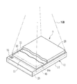
図3において、天板13の上面には光吸収層21が接着剤(図示せず)により貼り付けられている。光吸収層21の上には、放射線吸収部20が接着剤(図示せず)により貼り付けられている。光吸収層21及び放射線吸収部20は、照射面11を覆っている。これにより、放射線画像撮影装置7を薄型化し、かつ放射線検出器19を補強することができる。
In FIG. 3, a light absorbing layer 21 is attached to the top surface of the top plate 13 with an adhesive (not shown). The radiation absorbing portion 20 is attached onto the light absorbing layer 21 by an adhesive (not shown). The light absorbing layer 21 and the radiation absorbing unit 20 cover the irradiation surface 11. Thereby, the radiation imaging device 7 can be thinned and the radiation detector 19 can be reinforced.
FPD19は、放射線が照射される方向に沿って、天板13側から、センサパネル25とシンチレータ26とが順に積層されたものである。シンチレータ26の下面には、シンチレータ2を支持する支持基板27が設けられている。FPD19の外周には、シンチレータ26を湿気等から保護するために封止剤28が設けられている。筐体12内の底面には、FPD19の駆動回路基板29が配置されている。駆動回路基板29とセンサパネル25とは、フレキシブルケーブル30を介して電気的に接続されている。
The FPD 19 is one in which a sensor panel 25 and a scintillator 26 are sequentially stacked from the top 13 side along the direction in which the radiation is irradiated. A support substrate 27 supporting the scintillator 2 is provided on the lower surface of the scintillator 26. A sealing agent 28 is provided on the outer periphery of the FPD 19 in order to protect the scintillator 26 from moisture and the like. A drive circuit board 29 of the FPD 19 is disposed on the bottom of the housing 12. The drive circuit board 29 and the sensor panel 25 are electrically connected via the flexible cable 30.
シンチレータ26は、被写体Hを透過して筐体12の照射面11に照射され、天板13、放射線吸収部20、センサパネル25を透過して入射したX線を吸収して可視光を発生する。シンチレータ26としては、CsI:Tl(タリウムを添加したヨウ化セシウム)や、CsI:Na(ナトリウムを添加したヨウ化セシウム)、GOS(Gd2O2S:Tb)等が用いられる。本実施形態では、シンチレータ26として、CsI:Tlを用いる。シンチレータ26は、CsI:Tlを支持基板27に蒸着することにより形成される。このシンチレータ26は、柱状結晶構造であり、支持基板27からセンサパネル25に向かう方向に沿って、複数の柱状結晶(図示せず)を有している。柱状結晶は、その平径が柱状結晶の長手方向に沿ってほぼ均一である。
The scintillator 26 transmits the subject H and is irradiated to the irradiation surface 11 of the housing 12, and transmits the top plate 13, the radiation absorbing unit 20, and the sensor panel 25 to absorb incident X-rays and generate visible light. . As the scintillator 26, CsI: Tl (cesium iodide to which thallium is added), CsI: Na (cesium iodide to which sodium is added), GOS (Gd 2 O 2 S: Tb) or the like is used. In the present embodiment, CsI: Tl is used as the scintillator 26. The scintillator 26 is formed by vapor deposition of CsI: Tl on the support substrate 27. The scintillator 26 has a columnar crystal structure, and has a plurality of columnar crystals (not shown) along the direction from the support substrate 27 toward the sensor panel 25. The columnar crystal has a flat diameter substantially uniform along the longitudinal direction of the columnar crystal.
シンチレータ26で発生した光は、柱状結晶のライトガイド効果によって柱状結晶内を伝搬し、柱状結晶の先端部からセンサパネル25に向かって射出される。このように、シンチレータ26を柱状結晶構造とすることにより、シンチレータ26からセンサパネル25側へ射出される可視光の拡散が抑制されるので、放射線画像撮影装置7によって撮影される放射線画像の鮮鋭度が向上する。
The light generated by the scintillator 26 propagates in the columnar crystal due to the light guide effect of the columnar crystal, and is emitted toward the sensor panel 25 from the tip of the columnar crystal. As described above, by forming the scintillator 26 in a columnar crystal structure, diffusion of visible light emitted from the scintillator 26 to the sensor panel 25 side is suppressed, so the sharpness of the radiation image captured by the radiation imaging device 7 Improve.
支持基板27のシンチレータ26側の表面には、反射層(図示せず)が設けられている。シンチレータ26で発光し、支持基板27側に伝搬した可視光は、反射層によりセンサパネル25側へ反射されるので、センサパネル25への入射光量(シンチレータ26で発光した光の検出効率)が向上する。
A reflective layer (not shown) is provided on the surface of the support substrate 27 on the scintillator 26 side. The visible light emitted by the scintillator 26 and propagated to the support substrate 27 is reflected to the sensor panel 25 by the reflective layer, so the amount of light incident on the sensor panel 25 (detection efficiency of light emitted by the scintillator 26) is improved. Do.
X線によるシンチレータ26の発光は、主にシンチレータ26の表面側(X線入射側)で生じるため、本実施形態のように、シンチレータ26のX線入射側にセンサパネル25を配置した場合には、シンチレータ26での発光位置とセンサパネル25との距離が近いため、光検出の分解能及び受光量が高い。このように、シンチレータ26のX線入射側にセンサパネル25を配置する構成は、ISS(Irradiation Side Sampling)方式と称される。逆に、シンチレータのX線入射側とは反対側にセンサパネルを配置する構成は、PSS(Penetration Side Sampling)方式と称される。ISS方式では、PSS方式より放射線画像の鮮鋭度及び感度が向上する。
Since light emission of the scintillator 26 by X-rays mainly occurs on the surface side (X-ray incident side) of the scintillator 26, when the sensor panel 25 is disposed on the X-ray incident side of the scintillator 26 as in this embodiment Since the distance between the light emitting position of the scintillator 26 and the sensor panel 25 is short, the resolution of light detection and the amount of light received are high. As described above, the configuration in which the sensor panel 25 is disposed on the X-ray incident side of the scintillator 26 is referred to as an ISS (Irradiation Side Sampling) method. Conversely, a configuration in which the sensor panel is disposed on the opposite side to the X-ray incident side of the scintillator is called a PSS (Penetration Side Sampling) method. In the ISS method, the sharpness and sensitivity of the radiation image are improved compared to the PSS method.
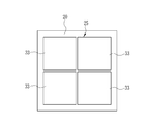
図4において、センサパネル25は、4枚のCMOS型イメージセンサ(以下、CMOSセンサという)33により構成されている。各CMOSセンサ33は、マトリクス状に配置された複数の画素33a(図7参照)を有する。各CMOSセンサ33は、一辺の長さが200mm程度の矩形状である。4枚のCMOSセンサ33は、上下左右に互いに隣接するように並べられ、およそ一辺が17インチの四角形を形成する。
In FIG. 4, the sensor panel 25 is configured by four CMOS type image sensors (hereinafter referred to as CMOS sensors) 33. Each CMOS sensor 33 has a plurality of pixels 33a (see FIG. 7) arranged in a matrix. Each CMOS sensor 33 has a rectangular shape with a side length of about 200 mm. The four CMOS sensors 33 are arranged adjacent to each other vertically and horizontally, and form a square of approximately 17 inches on a side.
CMOSセンサ33は、米国公開2009/0224162号公報に開示されたものと同様の構成である。具体的には、図5に示すように、CMOSセンサ33は、単結晶半導体基板34と、絶縁層35と、第1電極36と、光電変換層37と、第2電極38とにより構成されている。
The CMOS sensor 33 has a configuration similar to that disclosed in U.S. Patent Publication 2009/0224162. Specifically, as shown in FIG. 5, the CMOS sensor 33 is constituted of a single crystal semiconductor substrate 34, an insulating layer 35, a first electrode 36, a photoelectric conversion layer 37, and a second electrode 38. There is.
単結晶半導体基板34は、単結晶Siで作られている。絶縁層35は、単結晶半導体基板34の表面上に形成され、この絶縁層35には酸化シリコン等が用いられている。第1電極36は、絶縁層35の表面上に、画素33a毎に個別に形成されている。光電変換層37は、各第1電極36の表面上に、各画素33aに共通に設けられている。第2電極38は、光電変換層37の表面上に、各画素33aに共通に設けられている。第2電極38の表面上には、前述のシンチレータ26が接着剤(図示せず)により貼り合わされている。
The single crystal semiconductor substrate 34 is made of single crystal Si. The insulating layer 35 is formed on the surface of the single crystal semiconductor substrate 34, and silicon oxide or the like is used for the insulating layer 35. The first electrode 36 is individually formed for each pixel 33 a on the surface of the insulating layer 35. The photoelectric conversion layer 37 is provided on the surface of each first electrode 36 in common to each pixel 33 a. The second electrode 38 is provided on the surface of the photoelectric conversion layer 37 in common to each pixel 33 a. The aforementioned scintillator 26 is bonded onto the surface of the second electrode 38 by an adhesive (not shown).
第2電極38は、シンチレータ26で発生した可視光が光電変換層37に入射するように、可視光に対して透明な導電性材料(例えば、酸化インジウムスズ(ITO))で形成されている。本実施形態では、第2電極38を各画素33aに共通に設けているが、画素33a毎に個別に設けてもよい。
The second electrode 38 is formed of a conductive material (for example, indium tin oxide (ITO)) which is transparent to visible light so that visible light generated by the scintillator 26 is incident on the photoelectric conversion layer 37. In the present embodiment, the second electrode 38 is provided in common to each pixel 33a, but may be provided individually for each pixel 33a.
光電変換層37は、シンチレータ26との組み合わせにより、X線の入射量に応じた信号電荷を発生する。光電変換層37は、シンチレータ26により発生された可視光を吸収して、吸収した光量に応じた信号電荷を発生するものであり、有機又は無機の光電変換材料で形成されている。無機の光電変換材料としては、例えば、アモルファスシリコン(a-Si)がある。有機の光電変換材料としては、例えば、キナクリドンがある。
The photoelectric conversion layer 37 generates a signal charge according to the amount of incident X-rays, in combination with the scintillator 26. The photoelectric conversion layer 37 absorbs visible light generated by the scintillator 26, generates a signal charge according to the amount of absorbed light, and is formed of an organic or inorganic photoelectric conversion material. Examples of the inorganic photoelectric conversion material include amorphous silicon (a-Si). An example of the organic photoelectric conversion material is quinacridone.
図6に示すように、キナクリドンからなる有機光電変換材料(OPC)の感度は、CsI:Naや、単結晶Si(c-Si)よりも、CsI:Tlが発生する可視光の波長域に近い。このため、シンチレータ26としてCsI:Tlを用いた本実施形態では、光電変換層37をキナクリドンで形成することが好ましく、高い検出効率を得ることができる。
As shown in FIG. 6, the sensitivity of the organic photoelectric conversion material (OPC) made of quinacridone is closer to the wavelength range of visible light generated by CsI: Tl than by CsI: Na or single crystal Si (c-Si). . For this reason, in the present embodiment using CsI: Tl as the scintillator 26, it is preferable to form the photoelectric conversion layer 37 of quinacridone, and high detection efficiency can be obtained.
単結晶半導体基板34には、画素33a毎に信号出力回路41が設けられている。信号出力回路41は、CMOS回路により形成されている。信号出力回路41と第1電極36との間は、コンタクト配線42によって電気的に接続されている。第2電極38には、バイアス電圧が印加されており(図7参照)、光電変換層37により発生された信号電荷を各画素33aの第1電極36により収集する。信号出力回路41は、第1電極36により収集された信号電荷を、その信号電荷量に応じた電圧信号に変換して出力する。
In the single crystal semiconductor substrate 34, a signal output circuit 41 is provided for each pixel 33a. The signal output circuit 41 is formed of a CMOS circuit. The signal output circuit 41 and the first electrode 36 are electrically connected by the contact wiring 42. A bias voltage is applied to the second electrode 38 (see FIG. 7), and the signal charge generated by the photoelectric conversion layer 37 is collected by the first electrode 36 of each pixel 33 a. The signal output circuit 41 converts the signal charge collected by the first electrode 36 into a voltage signal corresponding to the signal charge amount and outputs the voltage signal.
図7において、信号出力回路41は、出力トランジスタT1、行選択トランジスタT2、リセットトランジスタT3、行選択線L1、信号出力線L2、リセット線L3により構成されている。出力トランジスタT1、行選択トランジスタT2、リセットトランジスタT3は、それぞれMOSトランジスタである。行選択線L1、信号出力線L2、リセット線L3は、前述の絶縁層35内にアルミニウム等の金属で形成されている。
In FIG. 7, the signal output circuit 41 includes an output transistor T1, a row selection transistor T2, a reset transistor T3, a row selection line L1, a signal output line L2, and a reset line L3. The output transistor T1, the row selection transistor T2, and the reset transistor T3 are each a MOS transistor. The row selection line L1, the signal output line L2, and the reset line L3 are formed of a metal such as aluminum in the insulating layer 35 described above.
出力トランジスタT1は、第1電極36に接続されており、第1電極36により収集された信号電荷に応じた電圧がゲートに印加される。行選択トランジスタT2は、行選択線L1に印加される選択信号よりオンとなり、出力トランジスタT1のゲート電圧に応じて制御された電圧信号が信号出力線L2に印加される。リセットトランジスタT3は、リセット線L3に印加される選択信号よりオンとなり、第1電極36により収集された信号電荷を電源配線Vddに破棄する。
The output transistor T1 is connected to the first electrode 36, and a voltage corresponding to the signal charge collected by the first electrode 36 is applied to the gate. The row selection transistor T2 is turned on by the selection signal applied to the row selection line L1, and a voltage signal controlled according to the gate voltage of the output transistor T1 is applied to the signal output line L2. The reset transistor T3 is turned on by the selection signal applied to the reset line L3, and discards the signal charge collected by the first electrode 36 to the power supply wiring Vdd.
以上のように、CMOSセンサ33の単結晶半導体基板34には、シリコンが用いられているため、各トランジスタT1~T3のキャリア移動度は、a-Si等の非晶質半導体からなるTFTに比べて、3~4桁以上高く、高速読み出しが可能である。また、単結晶半導体基板34には、FPD19の制御部等の周辺回路を混載することも可能である。
As described above, since silicon is used for the single crystal semiconductor substrate 34 of the CMOS sensor 33, the carrier mobility of each of the transistors T1 to T3 is higher than that of a TFT made of an amorphous semiconductor such as a-Si. Thus, high speed reading is possible by three to four digits or more. In addition, peripheral circuits such as a control unit of the FPD 19 can be mixedly mounted on the single crystal semiconductor substrate 34.
信号出力回路41のうち、行選択線L1、信号出力線L2、リセット線L3は、アルミニウム等の金属で形成されているためX線による劣化は少ないが、出力トランジスタT1、行選択トランジスタT2、リセットトランジスタT3は、単結晶Siで形成されているため、X線により特性が劣化(閾値電圧の変化や暗電流の増加)する恐れがある。これは、単結晶Siを用いたMOS構造では、X線の吸収によって単結晶半導体基板34と絶縁層35との界面に電荷(以下、界面電荷という)が生じて蓄積されるためである。
Of the signal output circuit 41, the row selection line L1, the signal output line L2, and the reset line L3 are formed of a metal such as aluminum, so there is little deterioration due to X-rays, but the output transistor T1, the row selection transistor T2, the reset Since the transistor T3 is formed of single crystal Si, there is a possibility that the characteristics may be degraded (change in threshold voltage or increase in dark current) due to X-rays. This is because in the MOS structure using single crystal Si, charges (hereinafter referred to as interface charge) are generated and accumulated at the interface between the single crystal semiconductor substrate 34 and the insulating layer 35 by absorption of X-rays.
放射線吸収部20は、天板13を透過したX線の一部(MOSトランジスタの特性劣化に影響する低エネルギ成分)を吸収する。X線の高エネルギ成分は、CMOSセンサ33を透過するが、X線の低エネルギ成分は、CMOSセンサ33を透過するだけのエネルギが無く、CMOSセンサ33に吸収されてしまうため、各トランジスタT1~T3の界面電荷を増加させる可能性がある。
The radiation absorbing portion 20 absorbs a part of the X-rays transmitted through the top plate 13 (a low energy component affecting the characteristic deterioration of the MOS transistor). The high energy component of the X-ray passes through the CMOS sensor 33, but the low energy component of the X-ray does not have enough energy to pass through the CMOS sensor 33, and is absorbed by the CMOS sensor 33. There is a possibility of increasing the interface charge of T3.
放射線吸収部20は、袋体47と放射線吸収性流動体48とで構成されている。袋体47は、被写体Hによる荷重により変形可能な弾力性を有する。放射線吸収性流動体48は、袋体47内に封入されている。袋体47は、例えば厚みが数mm~1cm程度のゴムやプラスチック材料等の弾力性を有する材質により袋状に形成されている。放射線吸収性流動体48は、液状またはジェル状であり、X線の一部(低エネルギ成分)を吸収する性質を有する。本実施形態では、放射線吸収性流動体48として、X線を吸収して光に変換する液状シンチレータを用いている。
The radiation absorbing portion 20 is composed of a bag 47 and a radiation absorbing fluid 48. The bag body 47 has elasticity that can be deformed by the load of the subject H. The radiation absorbing fluid 48 is enclosed in a bag 47. The bag body 47 is formed in a bag shape, for example, of an elastic material such as rubber or plastic material having a thickness of about several mm to 1 cm. The radiation absorbing fluid 48 is liquid or gel and has a property of absorbing a part of X-rays (low energy component). In the present embodiment, a liquid scintillator that absorbs X-rays and converts them into light is used as the radiation absorbing fluid 48.
液状シンチレータは、蛍光体からなる溶質、この溶質が混合される溶媒、界面活性剤などにより形成されている。液状シンチレータの特性は、溶媒、溶質、界面活性剤などの種類及び使用量に依存する。本実施形態では、溶媒として、例えば混合キシレン(異性体)、トルエン、プソイドクメン、ジオキサン等を用いる。また、溶質としては、例えばPPO、bulty-PBD、DMPOPOP、Bis-MSB等を用いる。これらの溶媒及び溶質を用い、溶質量を例えば0.5~5g/リットルにして液状シンチレータを構成する。例えば、溶質としてPPOを用いた場合には、440nm以下の発光スペクトルが得られる。なお、溶質内に波長変換材を混ぜることにより、発光スペクトルを長波側にシフトすることも可能である。
The liquid scintillator is formed of a solute composed of a phosphor, a solvent in which the solute is mixed, a surfactant, and the like. The properties of the liquid scintillator depend on the type and amount of solvent, solute, surfactant and the like. In the present embodiment, for example, mixed xylene (isomer), toluene, pseudocumene, dioxane or the like is used as the solvent. Further, as the solute, for example, PPO, bulty-PBD, DMPOPOP, Bis-MSB or the like is used. Using these solvents and solutes, the solution mass is, for example, 0.5 to 5 g / liter to construct a liquid scintillator. For example, when PPO is used as a solute, an emission spectrum of 440 nm or less is obtained. It is also possible to shift the emission spectrum to the long wave side by mixing a wavelength conversion material in the solute.
光吸収層21は、放射線吸収部20によってX線から変換された光を吸収することにより、放射線吸収部20の光がセンサパネル25に入射することを防止する。これにより、放射線画像の画質が防止される。光吸収層21は、液状シンチレータで発光した光を吸収可能な材質によって形成されている。
The light absorbing layer 21 absorbs the light converted from the X-rays by the radiation absorbing unit 20 to prevent the light of the radiation absorbing unit 20 from being incident on the sensor panel 25. This prevents the image quality of the radiation image. The light absorption layer 21 is formed of a material capable of absorbing light emitted by the liquid scintillator.
図8に示すように、被写体Hの撮影部位が手の場合には、撮影部位がFPD19の撮影範囲よりも小さい。また、このような場合には、撮影部位はFPD19の撮影範囲の中央に配置された状態で撮影されることがほとんどである。このため、撮影部位が配置される中央部以外の周縁部は、X線が直接FPD19に照射される素抜け領域となり、CMOSセンサ33において特性劣化が発生しやすい。したがって、FPD19に入射するX線は、放射線画像の画質に影響する中央部では放射線吸収部20によるX線の吸収量が少なく、一方の素抜け領域にあたる周縁部では放射線吸収部20によるX線の吸収量が多いことが好ましい。
As shown in FIG. 8, when the imaging region of the subject H is a hand, the imaging region is smaller than the imaging range of the FPD 19. Moreover, in such a case, the imaging region is mostly imaged in a state of being disposed at the center of the imaging range of the FPD 19. For this reason, the peripheral portion other than the central portion where the imaging region is arranged becomes a blank area where the X-rays are directly irradiated to the FPD 19, and characteristic deterioration easily occurs in the CMOS sensor 33. Therefore, the X-ray incident on the FPD 19 has a small amount of X-ray absorption by the radiation absorbing portion 20 in the central portion that affects the image quality of the radiation image, and in the peripheral portion corresponding to one missing region Preferably, the amount of absorption is large.
放射線吸収部20は、被写体Hの体重によって変形可能である。具体的には、図9に示すように、放射線吸収部20の中央部に被写体Hが載置された場合には、袋体47がその重さによって変形し、放射線吸収性流動体48が袋体47の変形に合わせて袋体47内で流動する。これにより、放射線吸収部20は、被写体Hの直下である中央部の厚みが薄くなり、周縁部の厚みが厚くなる。
The radiation absorbing unit 20 can be deformed by the weight of the subject H. Specifically, as shown in FIG. 9, when the subject H is placed at the central portion of the radiation absorbing unit 20, the bag 47 is deformed by its weight, and the radiation absorbing fluid 48 is a bag. It flows in the bag 47 in accordance with the deformation of the body 47. As a result, in the radiation absorbing unit 20, the thickness of the central portion immediately below the subject H is reduced, and the thickness of the peripheral portion is increased.
一般に、物体を透過した後のX線強度Iは、下記式(1)で示され、減弱係数μが一定であるときには、物体の厚みTが増加すると指数的に低下する。したがって、放射線吸収部20は、図9に示すように変形した場合には、周縁部のX線吸収量が高くなるため、素抜け領域におけるCMOSセンサ33の特性劣化が抑制される。また、放射線吸収部20の中央部におけるX線の吸収量は低下し、被写体Hが天板13と近接した状態となるので、放射線吸収部20によるX線散乱もほとんど生じることがなく、放射線画像の画質低下が抑制される。
In general, the X-ray intensity I after passing through the object is represented by the following equation (1), and decreases exponentially as the thickness T of the object increases when the attenuation coefficient μ is constant. Therefore, when the radiation absorbing portion 20 is deformed as shown in FIG. 9, the X-ray absorption amount at the peripheral portion becomes high, so that the characteristic deterioration of the CMOS sensor 33 in the blank area is suppressed. Further, the amount of absorption of X-rays at the central portion of the radiation absorbing portion 20 is reduced, and the subject H is in a state of being close to the top 13, so X-ray scattering by the radiation absorbing portion 20 hardly occurs. Image quality deterioration is suppressed.
I=I’exp(-μT)・・・(1)
I:透過後のX線強度
I’:透過前のX線強度
μ:減弱係数(物質の種類、密度で異なる)
T:透過厚み I = I'exp (-μT) (1)
I: X-ray intensity after transmission I ': X-ray intensity before transmission μ: Attenuation coefficient (different according to the type of substance and density)
T: Transmission thickness
I:透過後のX線強度
I’:透過前のX線強度
μ:減弱係数(物質の種類、密度で異なる)
T:透過厚み I = I'exp (-μT) (1)
I: X-ray intensity after transmission I ': X-ray intensity before transmission μ: Attenuation coefficient (different according to the type of substance and density)
T: Transmission thickness
上述したように、被写体Hの撮影を行う際には、天板13に被写体H自身の荷重が加わる。CMOSセンサ33の単結晶半導体基板34は、材質的に割れやすく、かつ厚みが数十μm程度と薄いため、天板13に加わった被写体Hの荷重による破損を防止する保護構造を有することが好ましい。特に、4枚のCMOSセンサ33で構成されたセンサパネル25では、センサパネル25の中央部に衝撃や荷重が加わると、4枚全てのCMOSセンサ33が破損することがあり、修理コストが非常に大きい。
As described above, when the subject H is photographed, the load of the subject H itself is applied to the top 13. Since the single crystal semiconductor substrate 34 of the CMOS sensor 33 is easily broken in material and thin as about several tens of μm, it is preferable that the single crystal semiconductor substrate 34 have a protective structure that prevents damage due to the load of the object H applied to the top plate 13 . In particular, in the sensor panel 25 configured of four CMOS sensors 33, when an impact or load is applied to the central portion of the sensor panel 25, all four CMOS sensors 33 may be damaged, and the repair cost is very high. large.
本実施形態では、放射線吸収部20が被写体Hからの荷重によって変形することにより、天板13の中央部に加わった荷重や衝撃を吸収するので、CMOSセンサ33の破損を防止することができる。また、放射線吸収部20により、被写体Hの熱がセンサパネル25に伝達されるのを抑制することができ、センサパネル25の温度むらによる放射線画像の画質劣化も抑制することができる。
In the present embodiment, the radiation absorbing portion 20 is deformed by the load from the subject H to absorb the load and the impact applied to the central portion of the top 13, so that the CMOS sensor 33 can be prevented from being damaged. In addition, the radiation absorbing unit 20 can suppress the heat of the subject H from being transmitted to the sensor panel 25, and can also suppress the image quality deterioration of the radiation image due to the temperature unevenness of the sensor panel 25.
図10において、放射線画像撮影装置7の電気回路は、センサパネル25、信号処理部50、画像メモリ51、制御部52、無線通信部53、バッテリ54等で構成されている。信号処理部50は、センサパネル25の各画素33aから出力された画素信号を増幅するアンプや、A/D(アナログ/デジタル)変換器等を備えており、センサパネル25から出力された画素信号をデジタルの画像データに変換する。
In FIG. 10, the electric circuit of the radiation image capturing apparatus 7 includes a sensor panel 25, a signal processing unit 50, an image memory 51, a control unit 52, a wireless communication unit 53, a battery 54 and the like. The signal processing unit 50 includes an amplifier for amplifying a pixel signal output from each pixel 33 a of the sensor panel 25, an A / D (analog / digital) converter, and the like, and the pixel signal output from the sensor panel 25 Into digital image data.
また、信号処理部50は、放射線吸収部20によるX線の低エネルギ成分の吸収分布に応じて放射線画像を補正する画像補正部50aを備えている。撮影部位は、中央部に載せられることが殆どであるから、撮影時には、放射線吸収部20の中央部が薄くなり、周縁部と比べてX吸収量が少ない。中央部の凹み状態は、撮影部位によって決まる。そこで、撮影部位に対する各部の厚みを実験的に求める。そして、この厚み量に応じた各画素または領域毎のX線吸収量を求めるための補正係数を画像補正部50aにセットしておく。こうすることにより、コンソール8で撮影部位を指定することによって、画像補正部50aは、補正係数を用いて画像データを補正することにより、放射線吸収部20のX線吸収量による影響を取り除く。なお、性別または体重と身長を入力することにより、補正の精度を向上させることができる。
The signal processing unit 50 further includes an image correction unit 50 a that corrects a radiation image according to the absorption distribution of low energy components of X-rays by the radiation absorption unit 20. Since the region to be imaged is mostly placed at the central portion, the central portion of the radiation absorbing unit 20 becomes thinner at the time of imaging, and the X absorption amount is smaller than that at the peripheral portion. The state of depression at the center depends on the imaging site. Therefore, the thickness of each part with respect to the imaging site is determined experimentally. Then, a correction coefficient for obtaining an X-ray absorption amount for each pixel or area corresponding to the thickness amount is set in the image correction unit 50a. By doing this, the image correction unit 50a corrects the image data using the correction coefficient by designating the imaging region with the console 8, thereby removing the influence of the X-ray absorption amount of the radiation absorption unit 20. The accuracy of the correction can be improved by inputting the gender or the weight and the height.
信号処理部50には画像メモリ51が接続されており、信号処理部50の画像補正部50aから出力された画像データは画像メモリ51に記憶される。画像メモリ51は複数フレーム分の画像データを記憶可能な記憶容量を有している。放射線画像の撮影が行われる毎に、撮影によって得られた画像データが画像メモリ51に順次記憶される。
An image memory 51 is connected to the signal processing unit 50, and the image data output from the image correction unit 50 a of the signal processing unit 50 is stored in the image memory 51. The image memory 51 has a storage capacity capable of storing image data of a plurality of frames. Image data obtained by imaging is sequentially stored in the image memory 51 each time a radiographic image is captured.
制御部52は、CPU52a、RAM52b、ROM52を有し、放射線画像撮影装置7の全体の動作を制御する。RAM52bは、DRAM等からなる一時記憶メモリである。ROM52は、フラッシュメモリ等からなる不揮発性メモリである。
The control unit 52 includes a CPU 52a, a RAM 52b, and a ROM 52, and controls the overall operation of the radiation imaging device 7. The RAM 52 b is a temporary storage memory made of a DRAM or the like. The ROM 52 is a non-volatile memory including a flash memory or the like.
無線通信部53は、IEEE(Institute of Electrical and Electronics
Engineers)802.11a/b/g/n等に代表される無線LAN(Local Area Network)規格に対応しており、外部機器との間での各種情報の無線通信を可能とする。制御部52は、無線通信部53を介してコンソール8と無線通信を行い、コンソール8との間で各種情報の送受信を行う。 Thewireless communication unit 53 is an IEEE (Institute of Electrical and Electronics).
Engineers) correspond to wireless LAN (Local Area Network) standards represented by 802.11a / b / g / n etc., and enable wireless communication of various information with external devices. Thecontrol unit 52 performs wireless communication with the console 8 via the wireless communication unit 53, and transmits and receives various types of information to and from the console 8.
Engineers)802.11a/b/g/n等に代表される無線LAN(Local Area Network)規格に対応しており、外部機器との間での各種情報の無線通信を可能とする。制御部52は、無線通信部53を介してコンソール8と無線通信を行い、コンソール8との間で各種情報の送受信を行う。 The
Engineers) correspond to wireless LAN (Local Area Network) standards represented by 802.11a / b / g / n etc., and enable wireless communication of various information with external devices. The
バッテリ54は、放射線画像撮影装置7内の各部に電力を供給する。バッテリ54は、充電可能な二次電池であり、また、放射線画像撮影装置7から着脱可能である。なお、信号処理部50、画像メモリ51、制御部52、無線通信部53を、駆動回路基板29内に設けることも可能である。これらはバスを介して互いに接続されている。
The battery 54 supplies power to each part in the radiation imaging device 7. The battery 54 is a rechargeable secondary battery, and is detachable from the radiation imaging device 7. The signal processing unit 50, the image memory 51, the control unit 52, and the wireless communication unit 53 may be provided in the drive circuit board 29. These are connected to one another via a bus.
図11において、コンソール8は、CPU57、ROM58、RAM59、HDD60を有しており、これらはバス67を介して互いに接続されている。CPU57は、コンソール8の各部を制御する。ROM58は、制御プログラムを含む各種プログラムを記憶している。RAM59は、各種データを一時的に記憶する。HDD60は、各種データを記憶する。
In FIG. 11, the console 8 includes a CPU 57, a ROM 58, a RAM 59, and an HDD 60, which are connected to one another via a bus 67. The CPU 57 controls each part of the console 8. The ROM 58 stores various programs including a control program. The RAM 59 temporarily stores various data. The HDD 60 stores various data.
また、バス67には、通信I/F61、無線通信部62、ディスプレイドライバ64、操作入力検出部66が接続されている。ディスプレイドライバ64には、ディスプレイ63が接続されている。操作入力検出部66には、操作パネル65が接続されている。
A communication I / F 61, a wireless communication unit 62, a display driver 64, and an operation input detection unit 66 are connected to the bus 67. A display 63 is connected to the display driver 64. An operation panel 65 is connected to the operation input detection unit 66.
通信I/F61は、接続端子61a、通信ケーブル69及び放射線発生装置6の接続端子70aを介して、放射線発生装置6の通信I/F70と接続されている。コンソール8のCPU57は、放射線発生装置6との間での曝射条件等の各種情報の送受信を通信I/F61経由で行う。無線通信部62は、放射線画像撮影装置7の無線通信部53と無線通信を行う機能を備えている。コンソール8のCPU57は、放射線画像撮影装置7との間で、画像データ等の各種情報の送受信を、無線通信部62を介して行う。
The communication I / F 61 is connected to the communication I / F 70 of the radiation generation device 6 via the connection terminal 61 a, the communication cable 69, and the connection terminal 70 a of the radiation generation device 6. The CPU 57 of the console 8 performs transmission and reception of various information such as the irradiation condition with the radiation generator 6 via the communication I / F 61. The wireless communication unit 62 has a function of performing wireless communication with the wireless communication unit 53 of the radiation image capturing apparatus 7. The CPU 57 of the console 8 exchanges various information such as image data with the radiation imaging device 7 via the wireless communication unit 62.
ディスプレイドライバ64は、ディスプレイ63への各種情報を表示させるための信号を生成して出力する。コンソール8のCPU57は、操作メニューや撮影された放射線画像等を、ディスプレイドライバ64を介してディスプレイ63に表示させる。また、操作パネル65は、複数のキーを有しており、各種の情報や操作指示を入力可能とする。操作入力検出部66は、操作パネル65に対してなされた操作を検出し、検出結果をCPU57に送信する。
The display driver 64 generates and outputs a signal for displaying various information on the display 63. The CPU 57 of the console 8 causes the display 63 to display the operation menu, the captured radiographic image, and the like via the display driver 64. Further, the operation panel 65 has a plurality of keys, and can input various information and operation instructions. The operation input detection unit 66 detects an operation performed on the operation panel 65, and transmits the detection result to the CPU 57.
放射線発生装置6は、通信I/F70と、線源制御部72と、放射線源6aとで構成されている。通信I/F70は、コンソール8との間で曝射条件等の各種情報の送受信を行う。線源制御部72は、コンソール8から受信した曝射条件(管電圧、管電流の情報を含む)に基づいて放射線源6aを制御する。
The radiation generating apparatus 6 is configured of a communication I / F 70, a radiation source control unit 72, and a radiation source 6a. The communication I / F 70 transmits and receives various information such as an irradiation condition to and from the console 8. The radiation source control unit 72 controls the radiation source 6 a based on the irradiation conditions (including the information of the tube voltage and the tube current) received from the console 8.
次に、放射線撮影システム5の作用を説明する。まず、撮影者(例えば放射線技師等)は、被写体Hの撮影部位と撮影台との間に、照射面11側を撮影部位に向けた状態で放射線画像撮影装置7を挿入する。次に、放射線画像撮影装置7の向きや位置等を細かく調整する。
Next, the operation of the radiation imaging system 5 will be described. First, the photographer (for example, a radiographer or the like) inserts the radiation imaging device 7 between the imaging region of the subject H and the imaging table with the irradiation surface 11 facing the imaging region. Next, the orientation, position, and the like of the radiation imaging device 7 are finely adjusted.
図8に示すように、放射線画像撮影装置7の上に撮影部位が直接載置される場合には、放射線画像撮影装置7には撮影部位を載置する際の衝撃や荷重が加わるが、この衝撃や荷重は、放射線吸収部20が変形することによって吸収される。本実施形態の放射線画像撮影装置7は、ISS方式であり、センサパネル25がシンチレータ26の天板13側に配置されているため、センサパネル25の破損が効果的に防止される。
As shown in FIG. 8, when the imaging region is directly placed on the radiation imaging device 7, the radiation imaging device 7 is subjected to an impact or a load when mounting the imaging region. The impact and load are absorbed by deformation of the radiation absorbing portion 20. The radiation image capturing apparatus 7 of the present embodiment is an ISS method, and the sensor panel 25 is disposed on the top plate 13 side of the scintillator 26, so that breakage of the sensor panel 25 is effectively prevented.
撮影者は、準備作業が完了すると、操作パネル65を操作して撮影開始を指示する。これにより、コンソール8では、曝射開始を指示する指示信号を放射線発生装置6へ送信し、放射線発生装置6は放射線源6aからX線を射出させる。放射線源6aから射出されたX線は、線源フィルタ6bにより低エネルギ成分が吸収され、被写体Hの撮影部位を透過し、放射線吸収部20及び光吸収層21を介して照射面11に照射される。そして、X線は、天板13及びセンサパネル25を透過して、シンチレータ26に入射する。
When the preparation work is completed, the photographer operates the operation panel 65 to instruct start of imaging. Thus, the console 8 transmits an instruction signal instructing the start of exposure to the radiation generator 6, and the radiation generator 6 causes the radiation source 6a to emit X-rays. The low energy component is absorbed by the radiation source filter 6b, the X-ray emitted from the radiation source 6a is transmitted through the imaging region of the subject H, and is irradiated to the irradiation surface 11 through the radiation absorbing portion 20 and the light absorbing layer 21. Ru. Then, the X-rays pass through the top plate 13 and the sensor panel 25 and enter the scintillator 26.
被写体Hを透過したX線は、放射線吸収部20により低エネルギ成分が吸収されるので、センサパネル25がX線を吸収することによる各CMOSセンサ33の特性劣化が抑制される。特に、放射線吸収部20は、被写体Hの重さによって変形することにより、中央部よりも周縁部の厚みが厚いため、周縁部(素抜け領域)にX線が直接照射されることによる特性劣化が効果的に抑制される。また、放射線吸収部20は、中央部の厚みが周縁部よりも薄いため、被写体Hの撮影部位を透過したX線が必要以上に吸収されることがなく、放射線画像の画質を大きく劣化させることはない。
The low energy component of the X-rays transmitted through the object H is absorbed by the radiation absorbing unit 20, so that the characteristic deterioration of each CMOS sensor 33 due to the sensor panel 25 absorbing the X-rays is suppressed. In particular, the radiation absorbing portion 20 is deformed by the weight of the object H, and the thickness of the peripheral portion is thicker than that of the central portion. Therefore, the characteristic deterioration due to direct irradiation of the X-ray to the peripheral portion Is effectively suppressed. In addition, since the radiation absorbing portion 20 has a central portion thinner than the peripheral portion, X-rays transmitted through the imaging region of the subject H are not absorbed more than necessary, and the image quality of the radiation image is greatly degraded. There is no.
シンチレータ26に入射したX線は、シンチレータ26のX線の入射面近傍、すなわちセンサパネル25側で大部分が可視光に変換される。シンチレータ26で発生した可視光のうち、センサパネル25側に向かって伝搬する可視光は、センサパネル25に入射する。また、シンチレータ26で発生した可視光のうち、支持基板27側に向かって伝搬した可視光は、支持基板27の反射層により反射された後、再びシンチレータ26を通ってセンサパネル25に向かい、センサパネル25に入射する。シンチレータ26で発光した可視光は、CsI:Tlからなる柱状結晶によってガイドされるので、画像ボケが抑制される。
Most of the X-rays incident on the scintillator 26 are converted into visible light in the vicinity of the X-ray incident surface of the scintillator 26, that is, on the sensor panel 25 side. Among the visible light generated by the scintillator 26, the visible light propagating toward the sensor panel 25 is incident on the sensor panel 25. Further, among the visible light generated by the scintillator 26, the visible light propagated toward the support substrate 27 is reflected by the reflective layer of the support substrate 27 and then passes through the scintillator 26 again toward the sensor panel 25, and the sensor The light is incident on the panel 25. Since the visible light emitted by the scintillator 26 is guided by the columnar crystal made of CsI: Tl, image blurring is suppressed.
シンチレータ26に入射した可視光は、第2電極38を透過して光電変換層37に入射し、光電変換層37で信号電荷に変換される。X線の曝射終了後、光電変換層37で発生した信号電荷は、第1電極36により収集され、X線の曝射終了後、信号出力回路41によって電圧信号に変換される。この電圧信号は、画素信号として各画素33aから順次出力される。出力された各画素信号は、信号処理部50により画像データに変換される。
The visible light incident on the scintillator 26 is transmitted through the second electrode 38 and incident on the photoelectric conversion layer 37, and is converted into signal charge by the photoelectric conversion layer 37. After the end of the X-ray emission, the signal charge generated in the photoelectric conversion layer 37 is collected by the first electrode 36 and converted to a voltage signal by the signal output circuit 41 after the end of the X-ray emission. This voltage signal is sequentially output from each pixel 33a as a pixel signal. The output pixel signals are converted into image data by the signal processing unit 50.
画像データは、画像補正部50aにより、放射線吸収部20の各部分の厚みによって変化するX線吸収量に応じて補正される。補正後の画像データは、画像メモリ51に記憶される。CPU52aは、画像メモリ51に記憶された画像データを、無線通信部53を介してコンソール8に送信する。コンソール8のCPU57は、放射線画像撮影装置7から受信した画像データを、RAM59を介してHDD60に記憶する。また、CPU57は、ディスプレイドライバ64を介して、HDD60に記憶されている画像データに基づく放射線画像を、ディスプレイ63に表示させる。
The image data is corrected by the image correction unit 50a according to the amount of X-ray absorption which changes with the thickness of each portion of the radiation absorption unit 20. The image data after correction is stored in the image memory 51. The CPU 52 a transmits the image data stored in the image memory 51 to the console 8 via the wireless communication unit 53. The CPU 57 of the console 8 stores the image data received from the radiation imaging device 7 in the HDD 60 via the RAM 59. Further, the CPU 57 causes the display 63 to display a radiation image based on the image data stored in the HDD 60 via the display driver 64.
上述したように、放射線吸収部20により、センサパネル25に入射するX線から低エネルギ成分が吸収されるので、CMOSセンサ33の特性劣化が抑制される。また、放射線画像撮影装置7上に載置される被写体Hの位置に応じて放射線吸収部20が変形し、低エネルギ成分の吸収量が変化するので、放射線画像の画質を劣化させることなく、素抜け領域におけるCMOSセンサ33の特性劣化が抑制される。これらの効果は、センサパネル25がシンチレータ26の天板13側に配置され、X線入射量の大きいISS方式において、特に顕著な効果が得られる。
As described above, since the low energy components from the X-rays incident on the sensor panel 25 are absorbed by the radiation absorbing unit 20, the characteristic deterioration of the CMOS sensor 33 is suppressed. In addition, the radiation absorbing unit 20 is deformed according to the position of the subject H placed on the radiation imaging device 7, and the amount of absorption of the low energy component changes, so that the image quality of the radiation image is not deteriorated. Characteristic deterioration of the CMOS sensor 33 in the missing region is suppressed. These effects are particularly remarkable in the ISS method in which the sensor panel 25 is disposed on the top plate 13 side of the scintillator 26 and the X-ray incident amount is large.
TFTパネルを用いた従来のISS方式の放射線画像撮影装置は、TFTパネルの基板として用いられる無アルカリガラスのX線吸収が大きいため、管電圧が低いマンモグラフィには適用が容易ではなかったが、本発明によればISS方式の放射線画像撮影装置にX線吸収が小さいCMOSセンサを用いることができるので、マンモグラフィへの適用が容易である。
The conventional ISS-type radiation imaging apparatus using a TFT panel is not easy to apply to mammography with a low tube voltage because the X-ray absorption of alkali-free glass used as a substrate of the TFT panel is large. According to the invention, since a CMOS sensor with low X-ray absorption can be used for a radiation imaging apparatus of ISS method, application to mammography is easy.
(その他の実施形態)
上記実施形態では、放射線吸収部20から放射される光を吸収するために光吸収層21を別途設けているが、袋体47の天板13との貼り合せ面、または袋体47全体に光吸収性を持たせてもよい。また、溶質の種類あるいは波長変換材を適宜選択することにより、放射線吸収性流動体48から放射される光の波長域と、センサパネル25が検出可能な波長域とを異ならせてもよい。これにより、光吸収層21を省略することができる。 (Other embodiments)
In the above embodiment, thelight absorbing layer 21 is separately provided to absorb the light emitted from the radiation absorbing unit 20, but the light is applied to the bonding surface of the bag 47 with the top plate 13 or the entire bag 47. It may have absorbency. The wavelength range of the light emitted from the radiation absorbing fluid 48 may be different from the wavelength range detectable by the sensor panel 25 by appropriately selecting the type of solute or the wavelength conversion material. Thereby, the light absorption layer 21 can be omitted.
上記実施形態では、放射線吸収部20から放射される光を吸収するために光吸収層21を別途設けているが、袋体47の天板13との貼り合せ面、または袋体47全体に光吸収性を持たせてもよい。また、溶質の種類あるいは波長変換材を適宜選択することにより、放射線吸収性流動体48から放射される光の波長域と、センサパネル25が検出可能な波長域とを異ならせてもよい。これにより、光吸収層21を省略することができる。 (Other embodiments)
In the above embodiment, the
また、上記実施形態では、放射線吸収性流動体48として液状シンチレータを用いているが、パラフィンシンチレータを用いてもよい。パラフィンシンチレータは、低温でワックス状であり、40°C程度で流動性が生じる。パラフィンシンチレータとしては、特開平07-301676号公報に詳しい記載があるため、詳細な説明は省略する。さらに、放射線吸収性流動体48として、ゲル化した水ガラス(ケイ酸ナトリウム)を用いてもよい。水ガラスのゲル化は、例えば、水ガラスに酸を加えて攪拌することにより生じる。
Further, in the above embodiment, a liquid scintillator is used as the radiation absorbing fluid 48, but a paraffin scintillator may be used. The paraffin scintillator is waxy at low temperature and has fluidity at about 40 ° C. The paraffin scintillator is described in detail in Japanese Patent Application Laid-Open No. 07-301676, so the detailed description is omitted. Furthermore, as the radiation absorbing fluid 48, gelled water glass (sodium silicate) may be used. The gelation of water glass occurs, for example, by adding an acid to water glass and stirring.
また、放射線吸収性流動体48を、液状またはジェル状の流動体中にX線吸収材を分散させて構成してもよい。このX線吸収材としては、X線の低エネルギ成分を吸収する効果が高く後方散乱が少ない、原子番号20~31の金属(例えば、銅)が好ましい。
Alternatively, the radiation absorbing fluid 48 may be configured by dispersing an X-ray absorbing material in a liquid or gel fluid. As this X-ray absorbing material, metals of atomic numbers 20 to 31 (for example, copper) having a high effect of absorbing low energy components of X-rays and little back scattering are preferable.
また、上記実施形態では、放射線吸収部20を、袋体47と放射線吸収性流動体48とで構成しているが、ゴム等の弾性体で形成してもよい。さらに、この弾性体中にX線吸収材を分散させてもよい。このX線吸収材としては、同様に原子番号20~31の金属が好ましい。
Moreover, in the said embodiment, although the radiation absorption part 20 is comprised with the bag body 47 and the radiation absorptive fluid body 48, you may form with elastic bodies, such as rubber | gum. Furthermore, an X-ray absorber may be dispersed in this elastic body. As this X-ray absorbing material, metals of atomic numbers 20 to 31 are similarly preferable.
また、上記実施形態では、放射線画像撮影装置7に1つの放射線吸収部20を設けているが、複数の放射線吸収部を設けてもよい。例えば、図12に示すように、放射線吸収部20に加えて、天板13とセンサパネル25との間に、X線の低エネルギ成分を吸収する板状の低エネルギ吸収板75を配置する。これにより、天板13上の放射線吸収部20が被写体Hの重さで変形した場合でも、FPD19の検出範囲全域においてX線の低エネルギ成分を少なくとも一定量吸収することができる。なお、低エネルギ吸収板75は、天板13と放射線吸収部20との間に配置してもよいし、天板13の代わりに低エネルギ吸収板75を用いてもよい。
Moreover, in the said embodiment, although the one radiation absorption part 20 is provided in the radiographic imaging apparatus 7, you may provide several radiation absorption parts. For example, as shown in FIG. 12, in addition to the radiation absorbing unit 20, a plate-like low energy absorbing plate 75 for absorbing low energy components of X-rays is disposed between the top plate 13 and the sensor panel 25. Thereby, even when the radiation absorbing portion 20 on the top 13 is deformed by the weight of the subject H, the low energy component of the X-ray can be absorbed at least a constant amount in the entire detection range of the FPD 19. The low energy absorbing plate 75 may be disposed between the top plate 13 and the radiation absorbing unit 20, or the low energy absorbing plate 75 may be used instead of the top plate 13.
低エネルギ吸収板75の材料には、例えば、アルミニウムやガラス等を用いることができるが、上述した線源フィルタ6bと同じ材料を含むようにしてもよい。線源フィルタ6bと放射線吸収部20とに同じ材料を用いることにより、透過するX線エネルギ分布が同じになる。こうすると、線源フィルタ6bを透過し得るX線が放射線吸収部20によっても吸収されにくいので、被写体Hの情報を含むX線が放射線吸収部20によって吸収されるのを抑制することができる。結果的にX線の利用効率が向上する。
As a material of the low energy absorbing plate 75, for example, aluminum, glass or the like can be used, but the same material as the above-mentioned source filter 6b may be included. By using the same material for the radiation source filter 6b and the radiation absorbing portion 20, the transmitted X-ray energy distribution becomes the same. In this case, X-rays that can pass through the radiation source filter 6b are difficult to be absorbed by the radiation absorbing unit 20 as well, so that it is possible to suppress X-rays including information of the object H from being absorbed by the radiation absorbing unit 20. As a result, the utilization efficiency of X-rays is improved.
また、CMOSセンサにフレキシブル性を付与するように、CMOSセンサを、プラスチックフイルム上に形成された有機薄膜トランジスタによって構成してもよい。有機薄膜トランジスタについては、「Tsuyoshi Sekitani、Flexible organic
transistors and circuits with extreme bending stability、Nature Materials 9、平成22年11月7日、p.1015-1022」において詳細に説明されているので、詳しい説明は省略する。 Further, the CMOS sensor may be configured by an organic thin film transistor formed on a plastic film so as to impart flexibility to the CMOS sensor. For organic thin film transistors, see “Tsuyoshi Sekitani, Flexible organic”.
Since this is described in detail in “Transistors and circuits with extreme bending stability, Nature Materials 9, November 7, 2010, pp. 1015-1022”, the detailed description will be omitted.
また、CMOSセンサにフレキシブル性を付与するには、フレキシブル性を有するプラスチック基板上に、単結晶Siによって形成されたフォトダイオード及びトランジスタを配置すればよい。プラスチック基板上へのフォトダイオード及びトランジスタの配置には、例えば、数十ミクロン程度の大きさのデバイスブロックを溶液中で散布し、基板上の必要な位置に配置する技術であるFAS(Fluidic Self-Assembly)法を用いることができる。なお、FSA法については、「前澤宏一、「Fluidic Self-Assemblyのための共鳴トンネルデバイスブロック作製技術」、電子情報通信学会技術研究報告 ED,電子デバイス、社団法人電子情報通信学会、平成20年6月6日、108巻、87号、p.67-71」において詳細に説明されているので、詳しい説明は省略する。
Further, in order to provide the CMOS sensor with flexibility, a photodiode and a transistor formed of single crystal Si may be provided over a flexible plastic substrate. For arrangement of photodiodes and transistors on a plastic substrate, for example, a device block of about several tens of microns in size is dispersed in a solution, and FAS (Fluidic Self- Assembly) can be used. Regarding the FSA method, "Koichi Maezawa," Resonant tunnel device block fabrication technology for Fluidic Self-Assembly ", Technical Report of IEICE, ED, Electronic Device, The Institute of Electronics, Information and Communication Engineers, 2008 6 May 6, 108, 87, p. Detailed description will be omitted as it is described in detail in 67-71.
また、上記実施形態では、センサパネルをCMOSセンサで構成しているが、本発明は、単結晶半導体基板により形成されたCCDイメージセンサでセンサパネルを構成した放射線画像撮影装置にも適用可能である。また、本発明は、ISS方式に限られず、PSS方式の放射線画像撮影装置にも適用可能である。さらに、本発明は、放射線を直接電荷に変換する直接変換型の放射線画像撮影装置にも適用が可能である。
Further, in the above embodiment, the sensor panel is constituted by a CMOS sensor, but the present invention is also applicable to a radiation image photographing apparatus in which the sensor panel is constituted by a CCD image sensor formed by a single crystal semiconductor substrate. . Further, the present invention is not limited to the ISS method, and is also applicable to a PSS type radiation imaging apparatus. Furthermore, the present invention is also applicable to a direct conversion type radiation imaging apparatus that converts radiation directly into electric charges.
また、上記実施形態では、FPDをカセッテサイズの筐体に組み込む例について説明したが、立位型、臥位型の撮影装置や、マンモグラフィ装置に組み込むことも可能である。また、本発明は、γ線など、X線以外の放射線を使用する放射線画像撮影装置にも適用可能である。上記実施形態で説明した本発明に係る放射線画像撮影装置の構成は一例であり、本発明の主旨を逸脱しない範囲内において適宜変更可能であることは言うまでもない。
Further, in the above embodiment, an example in which the FPD is incorporated into a cassette-sized casing has been described, but it is also possible to be incorporated into a standing-type or lying-down type imaging device or a mammography device. The present invention is also applicable to a radiation imaging apparatus using radiation other than X-rays, such as γ-rays. The configuration of the radiation image capturing apparatus according to the present invention described in the above embodiment is an example, and it goes without saying that the configuration can be appropriately changed without departing from the scope of the present invention.
Claims (20)
- 被写体を透過した放射線を検出して画像データを生成する放射線検出器と、
前記放射線検出器の放射線入射側に配置され、前記放射線検出器に入射する前記放射線の一部を吸収するとともに、被写体の荷重によって変形可能な放射線吸収部と、
を備えたことを特徴とする放射線画像撮影装置。 A radiation detector that detects radiation transmitted through an object and generates image data;
A radiation absorbing portion disposed on the radiation incident side of the radiation detector, absorbing a part of the radiation incident on the radiation detector, and being deformable by a load of an object;
A radiation image capturing apparatus comprising: - 前記放射線検出器は、単結晶半導体基板を有することを特徴とする請求の範囲第1項に記載の放射線画像撮影装置。 The radiation imaging device according to claim 1, wherein the radiation detector has a single crystal semiconductor substrate.
- 前記放射線吸収部は、袋体と、この袋体に封入された液状またはジェル状の放射線吸収性流動体とを有することを特徴とする請求の範囲第2項に記載の放射線画像撮影装置。 The radiation imaging apparatus according to claim 2, wherein the radiation absorbing portion includes a bag and a liquid or gel radiation absorbing fluid sealed in the bag.
- 前記放射線吸収性流動体は、前記放射線を吸収して光に変換する液状シンチレータであることを特徴とする請求の範囲第3項に記載の放射線画像撮影装置。 The radiation imaging apparatus according to claim 3, wherein the radiation absorbing fluid is a liquid scintillator which absorbs the radiation and converts it into light.
- 前記放射線検出器と前記放射線吸収部との間に、前記液状シンチレータにより変換された光を吸収する光吸収層を備えることを特徴とする請求の範囲第4項に記載の放射線画像撮影装置。 5. The radiation image capturing apparatus according to claim 4, further comprising a light absorbing layer for absorbing the light converted by the liquid scintillator, between the radiation detector and the radiation absorbing unit.
- 前記放射線吸収性流動体は、ゲル化された水ガラスであることを特徴とする請求の範囲第3項に記載の放射線画像撮影装置。 The radiation imaging apparatus according to claim 3, wherein the radiation absorbing fluid is gelled water glass.
- 前記放射線吸収性流動体は、液状またはジェル状の流動体と、前記流動体中に分散された放射線吸収材とを有することを特徴とする請求の範囲第3項に記載の放射線画像撮影装置。 The radiation imaging apparatus according to claim 3, wherein the radiation absorbing fluid has a liquid or gel fluid and a radiation absorbing material dispersed in the fluid.
- 前記放射線吸収部は、被写体からの荷重で変形する弾性体と、この弾性体中に分散された放射線吸収材とを有することを特徴とする請求の範囲第2項に記載の放射線画像撮影装置。 The radiation image capturing apparatus according to claim 2, wherein the radiation absorbing unit includes an elastic body that is deformed by a load from a subject, and a radiation absorbing material dispersed in the elastic body.
- 前記放射線吸収部を複数備えることを特徴とする請求の範囲第2項に記載の放射線画像撮影装置。 The radiation imaging device according to claim 2, comprising a plurality of the radiation absorption units.
- 前記放射線検出器は、前記放射線を吸収して光に変換するシンチレータと、前記シンチレータの放射線照射側に配置され、前記シンチレータにより変換された光を検出するセンサパネルとを有することとを特徴とする請求の範囲第2項に記載の放射線画像撮影装置。 The radiation detector includes a scintillator that absorbs the radiation and converts it into light, and a sensor panel that is disposed on the radiation irradiation side of the scintillator and detects light converted by the scintillator. The radiation imaging device according to claim 2.
- 前記シンチレータ及び前記センサパネルを収容する筐体を有し、この筐体上に前記放射線吸収部が取り付けられていることを特徴とする請求の範囲第10項に記載の放射線画像撮影装置。 11. The radiation image capturing apparatus according to claim 10, further comprising a case for accommodating the scintillator and the sensor panel, wherein the radiation absorbing unit is mounted on the case.
- 前記放射線吸収部は、袋体と、この袋体に封入された液状シンチレータとを有することを特徴とする請求の範囲第11項に記載の放射線画像撮影装置。 12. The radiation image capturing apparatus according to claim 11, wherein the radiation absorbing portion has a bag and a liquid scintillator enclosed in the bag.
- 前記センサパネルは、前記シンチレータにより変換された光を電荷に変換する光電変換層と、前記光電変換層で変換された電荷に応じた信号を出力する信号出力回路とを含む画素を複数有し、前記信号出力回路は、前記単結晶半導体基板に設けられていることを特徴とする請求の範囲第12項に記載の放射線画像撮影装置。 The sensor panel has a plurality of pixels including a photoelectric conversion layer that converts light converted by the scintillator into charge, and a signal output circuit that outputs a signal according to the charge converted by the photoelectric conversion layer. The radiation image photographing apparatus according to claim 12, wherein the signal output circuit is provided on the single crystal semiconductor substrate.
- 前記センサパネルは、CMOS型のイメージセンサにより構成されていることを特徴とする請求の範囲第13項に記載の放射線画像撮影装置。 The radiation image capturing apparatus according to claim 13, wherein the sensor panel is configured of a CMOS type image sensor.
- 前記光電変換層は、アモルファスシリコンまたはキナクリドンで形成されていることを特徴とする請求の範囲第14項に記載の放射線画像撮影装置。 The radiation image capturing apparatus according to claim 14, wherein the photoelectric conversion layer is formed of amorphous silicon or quinacridone.
- 前記液状シンチレータが発生する光の波長域は、前記センサパネルが検出可能な光の波長域と異なることを特徴とする請求の範囲第4項に記載の放射線画像撮影装置。 5. The radiation image capturing apparatus according to claim 4, wherein a wavelength range of light generated by the liquid scintillator is different from a wavelength range of light detectable by the sensor panel.
- 前記放射線吸収部は、前記放射線検出器よりもサイズが大きいことを特徴とする請求の範囲第2項に記載の放射線画像撮影装置。 The radiation imaging device according to claim 2, wherein the radiation absorbing unit is larger in size than the radiation detector.
- 前記放射線吸収部の放射線吸収量の領域差に応じて前記画像データを補正する画像補正部を備えることを特徴とする請求の範囲第2項に記載の放射線画像撮影装置。 The radiation image photographing apparatus according to claim 2, further comprising: an image correction unit that corrects the image data according to a region difference of the radiation absorption amount of the radiation absorption unit.
- 前記放射線吸収部は、前記放射線の低エネルギ成分を吸収することを特徴とする請求の範囲第2項に記載の放射線画像撮影装置。 The radiation imaging device according to claim 2, wherein the radiation absorbing unit absorbs a low energy component of the radiation.
- 前記放射線の低エネルギ成分は、前記放射線のエネルギ分布の1/2以下のエネルギ成分であることを特徴とする請求の範囲第19項に記載の放射線画像撮影装置。 20. The radiation imaging device according to claim 19, wherein the low energy component of the radiation is an energy component of 1/2 or less of the energy distribution of the radiation.
Applications Claiming Priority (2)
| Application Number | Priority Date | Filing Date | Title |
|---|---|---|---|
| JP2011-121967 | 2011-05-31 | ||
| JP2011121967A JP2012247402A (en) | 2011-05-31 | 2011-05-31 | Radiographic apparatus |
Publications (1)
| Publication Number | Publication Date |
|---|---|
| WO2012165156A1 true WO2012165156A1 (en) | 2012-12-06 |
Family
ID=47259019
Family Applications (1)
| Application Number | Title | Priority Date | Filing Date |
|---|---|---|---|
| PCT/JP2012/062624 WO2012165156A1 (en) | 2011-05-31 | 2012-05-17 | Radiation-image-capturing device |
Country Status (2)
| Country | Link |
|---|---|
| JP (1) | JP2012247402A (en) |
| WO (1) | WO2012165156A1 (en) |
Cited By (1)
| Publication number | Priority date | Publication date | Assignee | Title |
|---|---|---|---|---|
| CN108649004A (en) * | 2018-05-21 | 2018-10-12 | 王青 | A kind of litho machine wafer coating system |
Families Citing this family (1)
| Publication number | Priority date | Publication date | Assignee | Title |
|---|---|---|---|---|
| JP6264723B2 (en) * | 2013-01-23 | 2018-01-24 | コニカミノルタ株式会社 | Radiation imaging equipment |
Citations (10)
| Publication number | Priority date | Publication date | Assignee | Title |
|---|---|---|---|---|
| JPH05130990A (en) * | 1991-10-25 | 1993-05-28 | Hamamatsu Photonics Kk | X-ray image detector for medical treatment with automatic exposing function |
| JPH0727864A (en) * | 1993-07-14 | 1995-01-31 | Fuji Photo Film Co Ltd | Radiation detector |
| JPH11284909A (en) * | 1998-01-28 | 1999-10-15 | Canon Inc | Two-dimensional image pickup device |
| JP2003035781A (en) * | 2001-07-24 | 2003-02-07 | Canon Inc | Radiation image photographing device |
| JP2004505252A (en) * | 2000-07-21 | 2004-02-19 | トリクセル エス.アー.エス. | Radiation detector with extended service life |
| JP2005506552A (en) * | 2001-10-26 | 2005-03-03 | トリクセル エス.アー.エス. | Solid X-ray detector |
| JP2006058124A (en) * | 2004-08-19 | 2006-03-02 | Canon Inc | Cassette-type x-ray image photographing device |
| JP2007121100A (en) * | 2005-10-27 | 2007-05-17 | Hitachi Ltd | Support tool of female chest |
| JP2009212377A (en) * | 2008-03-05 | 2009-09-17 | Fujifilm Corp | Maging device and production method of imaging device |
| JP2011095281A (en) * | 2011-02-18 | 2011-05-12 | Konica Minolta Medical & Graphic Inc | Radiation image detector |
-
2011
- 2011-05-31 JP JP2011121967A patent/JP2012247402A/en not_active Withdrawn
-
2012
- 2012-05-17 WO PCT/JP2012/062624 patent/WO2012165156A1/en active Application Filing
Patent Citations (10)
| Publication number | Priority date | Publication date | Assignee | Title |
|---|---|---|---|---|
| JPH05130990A (en) * | 1991-10-25 | 1993-05-28 | Hamamatsu Photonics Kk | X-ray image detector for medical treatment with automatic exposing function |
| JPH0727864A (en) * | 1993-07-14 | 1995-01-31 | Fuji Photo Film Co Ltd | Radiation detector |
| JPH11284909A (en) * | 1998-01-28 | 1999-10-15 | Canon Inc | Two-dimensional image pickup device |
| JP2004505252A (en) * | 2000-07-21 | 2004-02-19 | トリクセル エス.アー.エス. | Radiation detector with extended service life |
| JP2003035781A (en) * | 2001-07-24 | 2003-02-07 | Canon Inc | Radiation image photographing device |
| JP2005506552A (en) * | 2001-10-26 | 2005-03-03 | トリクセル エス.アー.エス. | Solid X-ray detector |
| JP2006058124A (en) * | 2004-08-19 | 2006-03-02 | Canon Inc | Cassette-type x-ray image photographing device |
| JP2007121100A (en) * | 2005-10-27 | 2007-05-17 | Hitachi Ltd | Support tool of female chest |
| JP2009212377A (en) * | 2008-03-05 | 2009-09-17 | Fujifilm Corp | Maging device and production method of imaging device |
| JP2011095281A (en) * | 2011-02-18 | 2011-05-12 | Konica Minolta Medical & Graphic Inc | Radiation image detector |
Cited By (1)
| Publication number | Priority date | Publication date | Assignee | Title |
|---|---|---|---|---|
| CN108649004A (en) * | 2018-05-21 | 2018-10-12 | 王青 | A kind of litho machine wafer coating system |
Also Published As
| Publication number | Publication date |
|---|---|
| JP2012247402A (en) | 2012-12-13 |
Similar Documents
| Publication | Publication Date | Title |
|---|---|---|
| JP5693173B2 (en) | Radiation detection apparatus and radiation detection system | |
| US9592017B2 (en) | Radiographic imaging device and computer readable medium | |
| JP6033363B2 (en) | Radiation detection panel | |
| US8742356B2 (en) | Radiation image detecting device | |
| JP2012247281A (en) | Radiographic apparatus, scintillator, and method for manufacturing the same | |
| WO2012165155A1 (en) | Radiographic imaging device | |
| JP2011137804A (en) | Radiation imaging device | |
| JP5623316B2 (en) | Radiation imaging apparatus and manufacturing method | |
| WO2013015016A1 (en) | Radiographic equipment | |
| JP5624447B2 (en) | Radiation detection apparatus and scintillator panel manufacturing method | |
| US9006662B2 (en) | Radiological image detection device | |
| WO2012165156A1 (en) | Radiation-image-capturing device | |
| JP2012202735A (en) | Radiation imaging apparatus | |
| JP2011133859A (en) | Radiographic imaging apparatus | |
| JP2012013682A (en) | Radiographic image photographing device | |
| JP2011133465A (en) | Radiation imaging apparatus | |
| JP5638372B2 (en) | Radiation imaging equipment | |
| US20110012020A1 (en) | X-ray detector and method for fabricating the same | |
| JP5608533B2 (en) | Radiation imaging equipment | |
| JP5666276B2 (en) | Radiation imaging equipment | |
| JP5496938B2 (en) | Radiation image processing system, program, and defective pixel correction method | |
| WO2012029403A1 (en) | Radiation imaging system, radiation imaging device, and computer-readable recording medium | |
| JP2012093259A (en) | Radiography apparatus | |
| JP2011133441A (en) | Neutron beam detector and device for imaging neutron beam equipped with the same | |
| JP5608532B2 (en) | Radiation imaging equipment |
Legal Events
| Date | Code | Title | Description |
|---|---|---|---|
| 121 | Ep: the epo has been informed by wipo that ep was designated in this application |
Ref document number: 12793139 Country of ref document: EP Kind code of ref document: A1 |
|
| NENP | Non-entry into the national phase |
Ref country code: DE |
|
| 122 | Ep: pct application non-entry in european phase |
Ref document number: 12793139 Country of ref document: EP Kind code of ref document: A1 |