JP7190889B2 - 発光装置及び発光装置モジュール - Google Patents
発光装置及び発光装置モジュール Download PDFInfo
- Publication number
- JP7190889B2 JP7190889B2 JP2018229936A JP2018229936A JP7190889B2 JP 7190889 B2 JP7190889 B2 JP 7190889B2 JP 2018229936 A JP2018229936 A JP 2018229936A JP 2018229936 A JP2018229936 A JP 2018229936A JP 7190889 B2 JP7190889 B2 JP 7190889B2
- Authority
- JP
- Japan
- Prior art keywords
- light
- oxide particles
- coating
- emitting device
- metal oxide
- Prior art date
- Legal status (The legal status is an assumption and is not a legal conclusion. Google has not performed a legal analysis and makes no representation as to the accuracy of the status listed.)
- Active
Links
Images


Classifications
-
- H—ELECTRICITY
- H10—SEMICONDUCTOR DEVICES; ELECTRIC SOLID-STATE DEVICES NOT OTHERWISE PROVIDED FOR
- H10H—INORGANIC LIGHT-EMITTING SEMICONDUCTOR DEVICES HAVING POTENTIAL BARRIERS
- H10H20/00—Individual inorganic light-emitting semiconductor devices having potential barriers, e.g. light-emitting diodes [LED]
- H10H20/80—Constructional details
- H10H20/85—Packages
- H10H20/852—Encapsulations
- H10H20/854—Encapsulations characterised by their material, e.g. epoxy or silicone resins
-
- H—ELECTRICITY
- H10—SEMICONDUCTOR DEVICES; ELECTRIC SOLID-STATE DEVICES NOT OTHERWISE PROVIDED FOR
- H10H—INORGANIC LIGHT-EMITTING SEMICONDUCTOR DEVICES HAVING POTENTIAL BARRIERS
- H10H20/00—Individual inorganic light-emitting semiconductor devices having potential barriers, e.g. light-emitting diodes [LED]
- H10H20/80—Constructional details
- H10H20/85—Packages
- H10H20/851—Wavelength conversion means
- H10H20/8511—Wavelength conversion means characterised by their material, e.g. binder
- H10H20/8512—Wavelength conversion materials
- H10H20/8513—Wavelength conversion materials having two or more wavelength conversion materials
-
- H—ELECTRICITY
- H10—SEMICONDUCTOR DEVICES; ELECTRIC SOLID-STATE DEVICES NOT OTHERWISE PROVIDED FOR
- H10H—INORGANIC LIGHT-EMITTING SEMICONDUCTOR DEVICES HAVING POTENTIAL BARRIERS
- H10H20/00—Individual inorganic light-emitting semiconductor devices having potential barriers, e.g. light-emitting diodes [LED]
- H10H20/80—Constructional details
- H10H20/85—Packages
- H10H20/855—Optical field-shaping means, e.g. lenses
-
- H—ELECTRICITY
- H10—SEMICONDUCTOR DEVICES; ELECTRIC SOLID-STATE DEVICES NOT OTHERWISE PROVIDED FOR
- H10W—GENERIC PACKAGES, INTERCONNECTIONS, CONNECTORS OR OTHER CONSTRUCTIONAL DETAILS OF DEVICES COVERED BY CLASS H10
- H10W90/00—Package configurations
-
- H—ELECTRICITY
- H10—SEMICONDUCTOR DEVICES; ELECTRIC SOLID-STATE DEVICES NOT OTHERWISE PROVIDED FOR
- H10H—INORGANIC LIGHT-EMITTING SEMICONDUCTOR DEVICES HAVING POTENTIAL BARRIERS
- H10H20/00—Individual inorganic light-emitting semiconductor devices having potential barriers, e.g. light-emitting diodes [LED]
- H10H20/80—Constructional details
- H10H20/85—Packages
- H10H20/851—Wavelength conversion means
-
- H—ELECTRICITY
- H10—SEMICONDUCTOR DEVICES; ELECTRIC SOLID-STATE DEVICES NOT OTHERWISE PROVIDED FOR
- H10H—INORGANIC LIGHT-EMITTING SEMICONDUCTOR DEVICES HAVING POTENTIAL BARRIERS
- H10H20/00—Individual inorganic light-emitting semiconductor devices having potential barriers, e.g. light-emitting diodes [LED]
- H10H20/80—Constructional details
- H10H20/85—Packages
- H10H20/852—Encapsulations
- H10H20/853—Encapsulations characterised by their shape
-
- H—ELECTRICITY
- H10—SEMICONDUCTOR DEVICES; ELECTRIC SOLID-STATE DEVICES NOT OTHERWISE PROVIDED FOR
- H10H—INORGANIC LIGHT-EMITTING SEMICONDUCTOR DEVICES HAVING POTENTIAL BARRIERS
- H10H20/00—Individual inorganic light-emitting semiconductor devices having potential barriers, e.g. light-emitting diodes [LED]
- H10H20/80—Constructional details
- H10H20/882—Scattering means
Landscapes
- Led Device Packages (AREA)
- Inorganic Compounds Of Heavy Metals (AREA)
Description

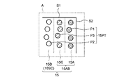
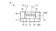
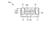
20 発光装置モジュール
11 基板
12 発光素子
14 透光部材
15、16、17 被覆体
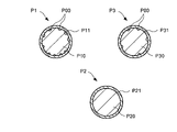
P1、P2、P3 酸化チタン粒子
15PT、16PT 粒子群
Claims (15)
- 基板と、
前記基板上に配置された発光素子と、
前記発光素子上に配置された透光部材と、
前記基板上において前記透光部材を取り囲むように配置され、前記透光部材の側面を覆う被覆体と、を有し、
前記被覆体は、前記被覆体内に分散された光散乱性の複数の金属酸化物粒子を含む粒子群を有し、
前記複数の金属酸化物粒子は、酸素欠損によってバンドギャップが低下する性質を有し、
前記粒子群における前記被覆体の側面の近傍に分散された前記複数の金属酸化物粒子は、各粒子内において、他の部分よりもバンドギャップが小さい部分を有することを特徴とする発光装置。 - 前記被覆体は、前記複数の金属酸化物粒子を担持し、可視光及び紫外光を透過させる1つの樹脂マトリクスを有することを特徴とする請求項1に記載の発光装置。
- 前記複数の金属酸化物粒子は、前記被覆体内において均一な密度で分散されていることを特徴とする請求項1又は2に記載の発光装置。
- 前記複数の金属酸化物粒子は、前記被覆体内において前記被覆体の上面から前記基板に向かって徐々に密度が高くなるように分散されていることを特徴とする請求項1又は2に記載の発光装置。
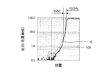
- 前記被覆体内における前記被覆体の側面の近傍の第1の領域に分散された前記複数の金属酸化物粒子における可視光の吸収率は、前記被覆体の前記第1の領域よりも内側の第2の領域に分散された前記複数の金属酸化物粒子における可視光の吸収率よりも大きいことを特徴とする請求項1乃至4のいずれか1つに記載の発光装置。
- 前記被覆体の前記第1の領域における前記複数の金属酸化物粒子を担持する樹脂マトリクスと、前記被覆体の前記第2の領域における前記複数の金属酸化物粒子を担持する樹脂マトリクスとが、連続して形成されている事を特徴とする請求項5に記載の発光装置。
- 前記複数の金属酸化物粒子は、酸化チタン粒子又は酸化亜鉛粒子を含むことを特徴とする請求項1乃至6のいずれか1つに記載の発光装置。
- 前記複数の金属酸化物粒子は、前記被覆体内において、5~70wt%の範囲内で分散されていることを特徴とする請求項1乃至7のいずれか1つに記載の発光装置。
- 前記粒子群は、前記複数の金属酸化物粒子と、前記複数の金属酸化物粒子を紫外線による変質から保護する被覆膜と、を有することを特徴とする請求項1乃至8のいずれか1つに記載の発光装置。
- 前記他の部分よりもバンドギャップが小さい部分を有する前記複数の金属酸化物粒子は、前記被覆体の側面から20μm以下の深さの範囲内の領域に分散されていることを特徴とする請求項7に記載の発光装置。
- モジュール基板及び前記モジュール基板上に並置された複数の発光装置を含み、
前記複数の発光装置の各々は、
個別基板と、
前記個別基板上に配置された発光素子と、
前記発光素子上に配置された透光部材と、
前記個別基板上において前記透光部材を取り囲むように配置され、前記透光部材の側面を覆う被覆体と、を有し、
前記被覆体は、光散乱性の複数の金属酸化物粒子を含む粒子群を有し、
前記複数の金属酸化物粒子は、酸素欠損によってバンドギャップが低下する性質を有し、
前記粒子群における前記被覆体の側面の近傍に分散された前記複数の金属酸化物粒子は、各粒子内において他の部分よりもバンドギャップが小さい部分を有することを特徴とする発光装置モジュール。 - 前記被覆体は、側面に複数の凹凸を有することを特徴とする請求項11に記載の発光装置モジュール。
- 基板と、
前記基板上に配置された発光素子と、
前記基板上において前記発光素子を取り囲むように配置され、前記発光素子の側面を覆う被覆体と、を有し、
前記被覆体は、光散乱性の複数の金属酸化物粒子を含む粒子群を有し、
前記複数の金属酸化物粒子は、酸素欠損によってバンドギャップが低下する性質を有し、
前記粒子群における前記被覆体の側面の近傍に分散された前記複数の金属酸化物粒子は、各粒子内において他の部分よりもバンドギャップが小さい部分を有することを特徴とする発光装置。 - 前記各粒子内における前記他の部分よりもバンドギャップが小さい部分の割合は、前記被覆体の側面の近傍に近づくにつれて増加する請求項1乃至13のいずれか1つに記載の発光装置。
- 基板と、
前記基板上に配置された発光素子と、
前記基板上において前記発光素子を取り囲むように配置され、前記発光素子の側面を覆う被覆体と、を有し、
前記被覆体は、光散乱性の複数の金属酸化物粒子を含む粒子群を有し、
前記複数の金属酸化物粒子は、酸素欠損によってバンドギャップが低下する性質を有し、
前記被覆体は、前記被覆体の側面に、前記複数の金属酸化物粒子に酸素欠損が生じるようにレーザ光が照射された領域を有することを特徴とする発光装置。
Priority Applications (2)
| Application Number | Priority Date | Filing Date | Title |
|---|---|---|---|
| JP2018229936A JP7190889B2 (ja) | 2018-12-07 | 2018-12-07 | 発光装置及び発光装置モジュール |
| US16/705,122 US11289629B2 (en) | 2018-12-07 | 2019-12-05 | Light-emitting device having covering body for supressing emission of stray light from side surfaces thereof, and light-emitting device module |
Applications Claiming Priority (1)
| Application Number | Priority Date | Filing Date | Title |
|---|---|---|---|
| JP2018229936A JP7190889B2 (ja) | 2018-12-07 | 2018-12-07 | 発光装置及び発光装置モジュール |
Publications (2)
| Publication Number | Publication Date |
|---|---|
| JP2020092230A JP2020092230A (ja) | 2020-06-11 |
| JP7190889B2 true JP7190889B2 (ja) | 2022-12-16 |
Family
ID=70970292
Family Applications (1)
| Application Number | Title | Priority Date | Filing Date |
|---|---|---|---|
| JP2018229936A Active JP7190889B2 (ja) | 2018-12-07 | 2018-12-07 | 発光装置及び発光装置モジュール |
Country Status (2)
| Country | Link |
|---|---|
| US (1) | US11289629B2 (ja) |
| JP (1) | JP7190889B2 (ja) |
Families Citing this family (5)
| Publication number | Priority date | Publication date | Assignee | Title |
|---|---|---|---|---|
| JP7570863B2 (ja) * | 2020-09-24 | 2024-10-22 | スタンレー電気株式会社 | 半導体発光装置及び半導体発光モジュール |
| JP7621783B2 (ja) | 2020-12-10 | 2025-01-27 | スタンレー電気株式会社 | 半導体発光装置及び半導体発光素子の支持基板 |
| JP7695805B2 (ja) * | 2021-03-10 | 2025-06-19 | スタンレー電気株式会社 | 発光装置及び発光装置の製造方法 |
| CN115775859B (zh) * | 2022-11-09 | 2026-02-17 | 京东方华灿光电(浙江)有限公司 | 改善光串扰的发光二极管及其制备方法 |
| JP7769239B2 (ja) * | 2023-09-29 | 2025-11-13 | 日亜化学工業株式会社 | 発光装置 |
Citations (10)
| Publication number | Priority date | Publication date | Assignee | Title |
|---|---|---|---|---|
| JP2002363379A (ja) | 2001-05-31 | 2002-12-18 | Nitto Denko Corp | 半導体封止用樹脂組成物およびそれを用いた半導体装置 |
| JP2009081235A (ja) | 2007-09-26 | 2009-04-16 | Osaka Univ | n型酸化物半導体の特性制御方法 |
| JP2010157638A (ja) | 2008-12-27 | 2010-07-15 | Nichia Corp | 発光装置及びその製造方法 |
| JP2012244062A (ja) | 2011-05-23 | 2012-12-10 | Hitachi Chem Co Ltd | 光半導体装置、光半導体素子搭載用基板及び光反射用熱硬化性樹脂組成物 |
| WO2013051600A1 (ja) | 2011-10-04 | 2013-04-11 | 株式会社カネカ | 硬化性樹脂組成物、硬化性樹脂組成物タブレット、成形体、半導体のパッケージ、半導体部品及び発光ダイオード |
| WO2014091539A1 (ja) | 2012-12-10 | 2014-06-19 | 株式会社エルム | 発光装置、led照明装置、および、前記発光装置に用いられる蛍光体含有フィルム片の製造方法 |
| JP2014236175A (ja) | 2013-06-05 | 2014-12-15 | 日亜化学工業株式会社 | 発光装置 |
| JP2016027620A (ja) | 2014-06-27 | 2016-02-18 | 日亜化学工業株式会社 | 発光装置 |
| US20160190400A1 (en) | 2013-05-13 | 2016-06-30 | Seoul Semiconductor Co., Ltd. | Light-emitting device package, manufacturing method thereof, and vehicle lamp and backlight unit including same |
| CN205846012U (zh) | 2016-05-18 | 2016-12-28 | 共青城超群科技股份有限公司 | 一种长寿无频闪的高聚光led封装 |
Family Cites Families (16)
| Publication number | Priority date | Publication date | Assignee | Title |
|---|---|---|---|---|
| DE102004049654B3 (de) * | 2004-10-11 | 2006-04-13 | Infineon Technologies Ag | Halbleiterbauteil mit Kunststoffgehäuse und Verfahren zur Herstellung desselben |
| US20070092737A1 (en) * | 2005-10-21 | 2007-04-26 | 3M Innovative Properties Company | Method of making light emitting device with silicon-containing encapsulant |
| DE102007021904A1 (de) * | 2007-02-28 | 2008-09-04 | Osram Opto Semiconductors Gmbh | Optoelektronische Vorrichtung mit Gehäusekörper |
| SG149709A1 (en) * | 2007-07-12 | 2009-02-27 | Micron Technology Inc | Microelectronic imagers and methods of manufacturing such microelectronic imagers |
| JP5326705B2 (ja) | 2009-03-17 | 2013-10-30 | 日亜化学工業株式会社 | 発光装置 |
| DE102009055786A1 (de) * | 2009-11-25 | 2011-05-26 | Osram Opto Semiconductors Gmbh | Gehäuse, optoelektronisches Bauteil und Verfahren zur Herstellung eines Gehäuses |
| CN103314038A (zh) * | 2010-12-08 | 2013-09-18 | 道康宁公司 | 适合形成封装物的包含金属氧化物纳米粒子的硅氧烷组合物 |
| TW201231311A (en) * | 2011-01-31 | 2012-08-01 | Sipix Chemical Inc | Decoration film and decorated molded device |
| US9205420B2 (en) * | 2011-04-22 | 2015-12-08 | President And Fellows Of Harvard College | Nanostructures, systems, and methods for photocatalysis |
| US9368748B2 (en) * | 2013-05-09 | 2016-06-14 | Shenzhen China Star Optoelectronics Technology Co., Ltd. | Display device and manufacturing method thereof |
| CN103456764B (zh) * | 2013-09-09 | 2016-01-20 | 京东方科技集团股份有限公司 | Oled阵列基板及其制造方法、显示装置 |
| GB201513272D0 (en) * | 2015-07-28 | 2015-09-09 | Isis Innovation | Luminescent material |
| KR102359594B1 (ko) * | 2017-09-19 | 2022-02-07 | 엘지디스플레이 주식회사 | 복합 무기 발광 재료, 발광 필름, 이를 포함하는 엘이디 패키지, 발광다이오드 및 발광장치 |
| US11357085B2 (en) * | 2017-09-25 | 2022-06-07 | Board Of Supervisors Of Louisiana State University And Agricultural And Mechanical College | Adaptive solid-state luminescent phosphors |
| US11024775B2 (en) * | 2017-10-17 | 2021-06-01 | Lumileds Llc | LED emitters with integrated nano-photonic structures to enhance EQE |
| US10991856B2 (en) * | 2017-12-21 | 2021-04-27 | Lumileds Llc | LED with structured layers and nanophosphors |
-
2018
- 2018-12-07 JP JP2018229936A patent/JP7190889B2/ja active Active
-
2019
- 2019-12-05 US US16/705,122 patent/US11289629B2/en active Active
Patent Citations (10)
| Publication number | Priority date | Publication date | Assignee | Title |
|---|---|---|---|---|
| JP2002363379A (ja) | 2001-05-31 | 2002-12-18 | Nitto Denko Corp | 半導体封止用樹脂組成物およびそれを用いた半導体装置 |
| JP2009081235A (ja) | 2007-09-26 | 2009-04-16 | Osaka Univ | n型酸化物半導体の特性制御方法 |
| JP2010157638A (ja) | 2008-12-27 | 2010-07-15 | Nichia Corp | 発光装置及びその製造方法 |
| JP2012244062A (ja) | 2011-05-23 | 2012-12-10 | Hitachi Chem Co Ltd | 光半導体装置、光半導体素子搭載用基板及び光反射用熱硬化性樹脂組成物 |
| WO2013051600A1 (ja) | 2011-10-04 | 2013-04-11 | 株式会社カネカ | 硬化性樹脂組成物、硬化性樹脂組成物タブレット、成形体、半導体のパッケージ、半導体部品及び発光ダイオード |
| WO2014091539A1 (ja) | 2012-12-10 | 2014-06-19 | 株式会社エルム | 発光装置、led照明装置、および、前記発光装置に用いられる蛍光体含有フィルム片の製造方法 |
| US20160190400A1 (en) | 2013-05-13 | 2016-06-30 | Seoul Semiconductor Co., Ltd. | Light-emitting device package, manufacturing method thereof, and vehicle lamp and backlight unit including same |
| JP2014236175A (ja) | 2013-06-05 | 2014-12-15 | 日亜化学工業株式会社 | 発光装置 |
| JP2016027620A (ja) | 2014-06-27 | 2016-02-18 | 日亜化学工業株式会社 | 発光装置 |
| CN205846012U (zh) | 2016-05-18 | 2016-12-28 | 共青城超群科技股份有限公司 | 一种长寿无频闪的高聚光led封装 |
Also Published As
| Publication number | Publication date |
|---|---|
| JP2020092230A (ja) | 2020-06-11 |
| US11289629B2 (en) | 2022-03-29 |
| US20200185574A1 (en) | 2020-06-11 |
Similar Documents
| Publication | Publication Date | Title |
|---|---|---|
| JP7190889B2 (ja) | 発光装置及び発光装置モジュール | |
| US10074786B2 (en) | LED with scattering features in substrate | |
| US9810402B2 (en) | Light conversion substrate and light emitting package and automobile lamp including the same | |
| KR20160036489A (ko) | 발광 장치 | |
| EP2223353B1 (en) | Side-emitting, light emitting device with hybrid, top scattering-reflector | |
| JP7190890B2 (ja) | 発光装置 | |
| JP7117170B2 (ja) | 発光装置 | |
| JP7387417B2 (ja) | 半導体発光装置 | |
| JP7277276B2 (ja) | 発光装置 | |
| US11067242B2 (en) | Phosphor module | |
| US10670211B2 (en) | Phosphor module | |
| EP2223351B1 (en) | Side emitting device with hybrid top reflector | |
| JP7161330B2 (ja) | 発光装置 | |
| JP7182450B2 (ja) | 発光装置 |
Legal Events
| Date | Code | Title | Description |
|---|---|---|---|
| A621 | Written request for application examination |
Free format text: JAPANESE INTERMEDIATE CODE: A621 Effective date: 20211102 |
|
| A977 | Report on retrieval |
Free format text: JAPANESE INTERMEDIATE CODE: A971007 Effective date: 20220720 |
|
| A131 | Notification of reasons for refusal |
Free format text: JAPANESE INTERMEDIATE CODE: A131 Effective date: 20220726 |
|
| A521 | Request for written amendment filed |
Free format text: JAPANESE INTERMEDIATE CODE: A523 Effective date: 20220920 |
|
| TRDD | Decision of grant or rejection written | ||
| A01 | Written decision to grant a patent or to grant a registration (utility model) |
Free format text: JAPANESE INTERMEDIATE CODE: A01 Effective date: 20221115 |
|
| A61 | First payment of annual fees (during grant procedure) |
Free format text: JAPANESE INTERMEDIATE CODE: A61 Effective date: 20221206 |
|
| R150 | Certificate of patent or registration of utility model |
Ref document number: 7190889 Country of ref document: JP Free format text: JAPANESE INTERMEDIATE CODE: R150 |
|
| R250 | Receipt of annual fees |
Free format text: JAPANESE INTERMEDIATE CODE: R250 |