JP7117136B2 - 発光素子及び発光装置 - Google Patents
発光素子及び発光装置 Download PDFInfo
- Publication number
- JP7117136B2 JP7117136B2 JP2018081721A JP2018081721A JP7117136B2 JP 7117136 B2 JP7117136 B2 JP 7117136B2 JP 2018081721 A JP2018081721 A JP 2018081721A JP 2018081721 A JP2018081721 A JP 2018081721A JP 7117136 B2 JP7117136 B2 JP 7117136B2
- Authority
- JP
- Japan
- Prior art keywords
- light
- translucent
- substrate
- emitting device
- covering member
- Prior art date
- Legal status (The legal status is an assumption and is not a legal conclusion. Google has not performed a legal analysis and makes no representation as to the accuracy of the status listed.)
- Active
Links
Images


Classifications
-
- H—ELECTRICITY
- H10—SEMICONDUCTOR DEVICES; ELECTRIC SOLID-STATE DEVICES NOT OTHERWISE PROVIDED FOR
- H10H—INORGANIC LIGHT-EMITTING SEMICONDUCTOR DEVICES HAVING POTENTIAL BARRIERS
- H10H20/00—Individual inorganic light-emitting semiconductor devices having potential barriers, e.g. light-emitting diodes [LED]
- H10H20/80—Constructional details
- H10H20/85—Packages
- H10H20/855—Optical field-shaping means, e.g. lenses
- H10H20/856—Reflecting means
-
- H—ELECTRICITY
- H10—SEMICONDUCTOR DEVICES; ELECTRIC SOLID-STATE DEVICES NOT OTHERWISE PROVIDED FOR
- H10H—INORGANIC LIGHT-EMITTING SEMICONDUCTOR DEVICES HAVING POTENTIAL BARRIERS
- H10H20/00—Individual inorganic light-emitting semiconductor devices having potential barriers, e.g. light-emitting diodes [LED]
- H10H20/80—Constructional details
- H10H20/81—Bodies
- H10H20/819—Bodies characterised by their shape, e.g. curved or truncated substrates
- H10H20/82—Roughened surfaces, e.g. at the interface between epitaxial layers
-
- H—ELECTRICITY
- H10—SEMICONDUCTOR DEVICES; ELECTRIC SOLID-STATE DEVICES NOT OTHERWISE PROVIDED FOR
- H10H—INORGANIC LIGHT-EMITTING SEMICONDUCTOR DEVICES HAVING POTENTIAL BARRIERS
- H10H20/00—Individual inorganic light-emitting semiconductor devices having potential barriers, e.g. light-emitting diodes [LED]
- H10H20/80—Constructional details
- H10H20/85—Packages
- H10H20/851—Wavelength conversion means
- H10H20/8514—Wavelength conversion means characterised by their shape, e.g. plate or foil
-
- H—ELECTRICITY
- H10—SEMICONDUCTOR DEVICES; ELECTRIC SOLID-STATE DEVICES NOT OTHERWISE PROVIDED FOR
- H10H—INORGANIC LIGHT-EMITTING SEMICONDUCTOR DEVICES HAVING POTENTIAL BARRIERS
- H10H20/00—Individual inorganic light-emitting semiconductor devices having potential barriers, e.g. light-emitting diodes [LED]
- H10H20/80—Constructional details
- H10H20/85—Packages
- H10H20/852—Encapsulations
-
- H10W90/00—
-
- H—ELECTRICITY
- H10—SEMICONDUCTOR DEVICES; ELECTRIC SOLID-STATE DEVICES NOT OTHERWISE PROVIDED FOR
- H10H—INORGANIC LIGHT-EMITTING SEMICONDUCTOR DEVICES HAVING POTENTIAL BARRIERS
- H10H20/00—Individual inorganic light-emitting semiconductor devices having potential barriers, e.g. light-emitting diodes [LED]
- H10H20/80—Constructional details
- H10H20/84—Coatings, e.g. passivation layers or antireflective coatings
-
- H—ELECTRICITY
- H10—SEMICONDUCTOR DEVICES; ELECTRIC SOLID-STATE DEVICES NOT OTHERWISE PROVIDED FOR
- H10H—INORGANIC LIGHT-EMITTING SEMICONDUCTOR DEVICES HAVING POTENTIAL BARRIERS
- H10H20/00—Individual inorganic light-emitting semiconductor devices having potential barriers, e.g. light-emitting diodes [LED]
- H10H20/80—Constructional details
- H10H20/85—Packages
- H10H20/851—Wavelength conversion means
- H10H20/8511—Wavelength conversion means characterised by their material, e.g. binder
- H10H20/8512—Wavelength conversion materials
-
- H—ELECTRICITY
- H10—SEMICONDUCTOR DEVICES; ELECTRIC SOLID-STATE DEVICES NOT OTHERWISE PROVIDED FOR
- H10H—INORGANIC LIGHT-EMITTING SEMICONDUCTOR DEVICES HAVING POTENTIAL BARRIERS
- H10H20/00—Individual inorganic light-emitting semiconductor devices having potential barriers, e.g. light-emitting diodes [LED]
- H10H20/80—Constructional details
- H10H20/882—Scattering means
Landscapes
- Engineering & Computer Science (AREA)
- Power Engineering (AREA)
- Microelectronics & Electronic Packaging (AREA)
- Led Device Packages (AREA)
- Physics & Mathematics (AREA)
- Condensed Matter Physics & Semiconductors (AREA)
- General Physics & Mathematics (AREA)
- Computer Hardware Design (AREA)
Description
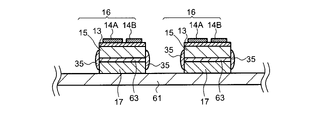
図4Bは、実施例4の変形例である発光装置50の断面を示す断面図である。発光装置50は、発光素子52を有している。発光装置50は、発光素子52が反射膜43の代わりに金属膜を含む部材として、遮光部材21及び反射膜53を有している点において実施例4の発光装置40と異なり、その余の点については同様に構成されている。
11 実装基板
12、32A、32B、42、52 発光素子
13 半導体構造層
13B 発光層
15 透光性基板
17 波長変換層
19、33、35 透光性被覆部材
21 遮光部材
43、53 反射膜
Claims (11)
- 発光層を有する半導体構造層と、
前記半導体構造層上に設けられた透光性基板と、
前記透光性基板上に配された波長変換層と、
前記透光性基板の側面の少なくとも一部を被覆し、かつ、前記発光層からの光に対する透過性を有する透光性被覆部材と、
前記透光性被覆部材の表面を含み、前記半導体構造層の側面、前記透光性基板の側面及び前記波長変換層の側面からなる面を全体に亘って覆うように形成された遮光部材と、を有し、
前記透光性基板の前記側面は、サブミクロンオーダの錐状凹凸が広がって分布した粗面領域を有する発光素子。 - 前記粗面領域は、前記透光性基板の基板面に平行な方向に沿って前記錐状凹凸が密集している帯状領域を有する請求項1に記載の発光素子。
- 前記透光性被覆部材は、少なくとも前記波長変換層の側面と前記透光性基板の側面との境界から、前記半導体構造層の側面の下端に亘って一体的に被覆している請求項1又は2に記載の発光素子。
- 前記透光性被覆部材は、少なくとも前記波長変換層の側面と前記透光性基板の側面との境界から、前記透光性基板の下端に至らない位置にかけて、前記透光性基板の側面を被覆している請求項1乃至3のいずれか1つに記載の発光素子。
- 前記透光性被覆部材は、前記透光性基板の側面の前記粗面領域を被覆している請求項1又は2に記載の発光素子。
- 前記透光性被覆部材は、前記透光性基板の側面の前記帯状領域を被覆している請求項2に記載の発光素子。
- 前記透光性被覆部材は、前記透光性基板の側面の前記錐状凹凸の凹部に気泡を含む請求項1乃至6のいずれか1つに記載の発光素子。
- 前記遮光部材は光散乱材を含む請求項1乃至7のいずれか1つに記載の発光素子。
- 前記遮光部材は金属膜である請求項1乃至8のいずれか1つに記載の発光素子。
- 前記遮光部材は金属膜を含む部材である請求項1乃至9のいずれか1つに記載の発光素子。
- 実装面と、
前記実装面上に並置されて配列された請求項1に記載の発光素子の複数と、
を含む発光装置。
Priority Applications (2)
| Application Number | Priority Date | Filing Date | Title |
|---|---|---|---|
| JP2018081721A JP7117136B2 (ja) | 2018-04-20 | 2018-04-20 | 発光素子及び発光装置 |
| US16/389,455 US10978627B2 (en) | 2018-04-20 | 2019-04-19 | Light-emitting element and light-emitting device |
Applications Claiming Priority (1)
| Application Number | Priority Date | Filing Date | Title |
|---|---|---|---|
| JP2018081721A JP7117136B2 (ja) | 2018-04-20 | 2018-04-20 | 発光素子及び発光装置 |
Publications (2)
| Publication Number | Publication Date |
|---|---|
| JP2019192716A JP2019192716A (ja) | 2019-10-31 |
| JP7117136B2 true JP7117136B2 (ja) | 2022-08-12 |
Family
ID=68238193
Family Applications (1)
| Application Number | Title | Priority Date | Filing Date |
|---|---|---|---|
| JP2018081721A Active JP7117136B2 (ja) | 2018-04-20 | 2018-04-20 | 発光素子及び発光装置 |
Country Status (2)
| Country | Link |
|---|---|
| US (1) | US10978627B2 (ja) |
| JP (1) | JP7117136B2 (ja) |
Families Citing this family (5)
| Publication number | Priority date | Publication date | Assignee | Title |
|---|---|---|---|---|
| TWI838548B (zh) * | 2020-06-24 | 2024-04-11 | 方略電子股份有限公司 | 發光裝置 |
| CN114178710B (zh) * | 2020-08-24 | 2024-11-26 | 奥特斯(中国)有限公司 | 部件承载件及其制造方法 |
| JP7570863B2 (ja) * | 2020-09-24 | 2024-10-22 | スタンレー電気株式会社 | 半導体発光装置及び半導体発光モジュール |
| JP7621783B2 (ja) | 2020-12-10 | 2025-01-27 | スタンレー電気株式会社 | 半導体発光装置及び半導体発光素子の支持基板 |
| JP7513907B2 (ja) | 2021-12-24 | 2024-07-10 | 日亜化学工業株式会社 | 発光装置 |
Citations (5)
| Publication number | Priority date | Publication date | Assignee | Title |
|---|---|---|---|---|
| WO2014034131A1 (ja) | 2012-08-31 | 2014-03-06 | パナソニック株式会社 | 発光装置 |
| JP2015023162A (ja) | 2013-07-19 | 2015-02-02 | 日亜化学工業株式会社 | 発光装置 |
| US20170005245A1 (en) | 2015-07-02 | 2017-01-05 | Xiamen Sanan Optoelectronics Technology Co., Ltd. | Light Emitting Diode Package Structure and Fabrication Method |
| JP2017033967A (ja) | 2015-07-28 | 2017-02-09 | 日亜化学工業株式会社 | 発光装置及びその製造方法 |
| JP2017157723A (ja) | 2016-03-02 | 2017-09-07 | 日亜化学工業株式会社 | 発光装置及びその製造方法 |
Family Cites Families (7)
| Publication number | Priority date | Publication date | Assignee | Title |
|---|---|---|---|---|
| JP4474892B2 (ja) | 2003-10-14 | 2010-06-09 | 日亜化学工業株式会社 | フリップチップ型led |
| US10043946B2 (en) * | 2009-08-25 | 2018-08-07 | Soraa, Inc. | Methods and devices for light extraction from a group III-nitride volumetric LED using surface and sidewall roughening |
| KR101047639B1 (ko) * | 2010-04-19 | 2011-07-07 | 엘지이노텍 주식회사 | 반도체 발광소자, 발광 소자 패키지 및 반도체 발광 소자 제조방법 |
| TWI543395B (zh) * | 2013-04-01 | 2016-07-21 | 中國砂輪企業股份有限公司 | 圖案化光電基板及其製作方法 |
| KR20150112237A (ko) * | 2014-03-27 | 2015-10-07 | 서울바이오시스 주식회사 | 발광 소자의 제조 방법 및 그것에 의해 제조된 발광 소자 |
| JP6288009B2 (ja) * | 2015-08-31 | 2018-03-07 | 日亜化学工業株式会社 | 発光装置の製造方法 |
| CN111525008B (zh) * | 2017-02-17 | 2023-07-25 | 首尔伟傲世有限公司 | 具有侧面反射层的发光二极管 |
-
2018
- 2018-04-20 JP JP2018081721A patent/JP7117136B2/ja active Active
-
2019
- 2019-04-19 US US16/389,455 patent/US10978627B2/en active Active
Patent Citations (5)
| Publication number | Priority date | Publication date | Assignee | Title |
|---|---|---|---|---|
| WO2014034131A1 (ja) | 2012-08-31 | 2014-03-06 | パナソニック株式会社 | 発光装置 |
| JP2015023162A (ja) | 2013-07-19 | 2015-02-02 | 日亜化学工業株式会社 | 発光装置 |
| US20170005245A1 (en) | 2015-07-02 | 2017-01-05 | Xiamen Sanan Optoelectronics Technology Co., Ltd. | Light Emitting Diode Package Structure and Fabrication Method |
| JP2017033967A (ja) | 2015-07-28 | 2017-02-09 | 日亜化学工業株式会社 | 発光装置及びその製造方法 |
| JP2017157723A (ja) | 2016-03-02 | 2017-09-07 | 日亜化学工業株式会社 | 発光装置及びその製造方法 |
Also Published As
| Publication number | Publication date |
|---|---|
| US20190326491A1 (en) | 2019-10-24 |
| US10978627B2 (en) | 2021-04-13 |
| JP2019192716A (ja) | 2019-10-31 |
Similar Documents
| Publication | Publication Date | Title |
|---|---|---|
| US10074786B2 (en) | LED with scattering features in substrate | |
| JP7117136B2 (ja) | 発光素子及び発光装置 | |
| JP6724933B2 (ja) | 発光装置の製造方法 | |
| US10429011B2 (en) | Method of manufacturing light emitting device | |
| JP5915483B2 (ja) | 発光装置及びその製造方法 | |
| JP6213582B2 (ja) | 発光装置 | |
| JP2016219743A (ja) | 発光装置 | |
| JP2013110154A (ja) | 発光装置 | |
| TW201611339A (zh) | 半導體發光裝置 | |
| WO2016093325A1 (ja) | 発光装置 | |
| US11063190B2 (en) | Light-emitting diode package component | |
| JP2019186236A (ja) | 発光装置 | |
| KR101364720B1 (ko) | 분포 브래그 반사기를 갖는 발광 다이오드 | |
| US9978734B2 (en) | Light-emitting arrangement and method of producing a light-emitting arrangement | |
| JP5970215B2 (ja) | 発光装置およびその製造方法 | |
| JP6383539B2 (ja) | 発光装置 | |
| JP2022021300A (ja) | 発光モジュールおよび面状光源 | |
| US20160079487A1 (en) | Semiconductor light-emitting device | |
| KR102519814B1 (ko) | 높은 근거리 콘트라스트 비를 갖는 led 모듈 | |
| JP2019012860A (ja) | 発光装置 | |
| JP7484075B2 (ja) | 発光モジュールの製造方法 | |
| JP4861474B2 (ja) | 発光装置 | |
| JP2010153595A (ja) | 発光装置 | |
| KR20140026153A (ko) | 반도체 소자 구조물 |
Legal Events
| Date | Code | Title | Description |
|---|---|---|---|
| A621 | Written request for application examination |
Free format text: JAPANESE INTERMEDIATE CODE: A621 Effective date: 20210316 |
|
| A131 | Notification of reasons for refusal |
Free format text: JAPANESE INTERMEDIATE CODE: A131 Effective date: 20220222 |
|
| A977 | Report on retrieval |
Free format text: JAPANESE INTERMEDIATE CODE: A971007 Effective date: 20220222 |
|
| A521 | Request for written amendment filed |
Free format text: JAPANESE INTERMEDIATE CODE: A523 Effective date: 20220420 |
|
| A131 | Notification of reasons for refusal |
Free format text: JAPANESE INTERMEDIATE CODE: A131 Effective date: 20220614 |
|
| A521 | Request for written amendment filed |
Free format text: JAPANESE INTERMEDIATE CODE: A523 Effective date: 20220628 |
|
| TRDD | Decision of grant or rejection written | ||
| A01 | Written decision to grant a patent or to grant a registration (utility model) |
Free format text: JAPANESE INTERMEDIATE CODE: A01 Effective date: 20220705 |
|
| A61 | First payment of annual fees (during grant procedure) |
Free format text: JAPANESE INTERMEDIATE CODE: A61 Effective date: 20220801 |
|
| R150 | Certificate of patent or registration of utility model |
Ref document number: 7117136 Country of ref document: JP Free format text: JAPANESE INTERMEDIATE CODE: R150 |
|
| R250 | Receipt of annual fees |
Free format text: JAPANESE INTERMEDIATE CODE: R250 |