JP7098677B2 - 基板処理装置、半導体装置の製造方法及びプログラム - Google Patents
基板処理装置、半導体装置の製造方法及びプログラム Download PDFInfo
- Publication number
- JP7098677B2 JP7098677B2 JP2020054334A JP2020054334A JP7098677B2 JP 7098677 B2 JP7098677 B2 JP 7098677B2 JP 2020054334 A JP2020054334 A JP 2020054334A JP 2020054334 A JP2020054334 A JP 2020054334A JP 7098677 B2 JP7098677 B2 JP 7098677B2
- Authority
- JP
- Japan
- Prior art keywords
- region
- substrate
- purge
- pressure
- processing
- Prior art date
- Legal status (The legal status is an assumption and is not a legal conclusion. Google has not performed a legal analysis and makes no representation as to the accuracy of the status listed.)
- Active
Links
Images


Classifications
-
- C—CHEMISTRY; METALLURGY
- C23—COATING METALLIC MATERIAL; COATING MATERIAL WITH METALLIC MATERIAL; CHEMICAL SURFACE TREATMENT; DIFFUSION TREATMENT OF METALLIC MATERIAL; COATING BY VACUUM EVAPORATION, BY SPUTTERING, BY ION IMPLANTATION OR BY CHEMICAL VAPOUR DEPOSITION, IN GENERAL; INHIBITING CORROSION OF METALLIC MATERIAL OR INCRUSTATION IN GENERAL
- C23C—COATING METALLIC MATERIAL; COATING MATERIAL WITH METALLIC MATERIAL; SURFACE TREATMENT OF METALLIC MATERIAL BY DIFFUSION INTO THE SURFACE, BY CHEMICAL CONVERSION OR SUBSTITUTION; COATING BY VACUUM EVAPORATION, BY SPUTTERING, BY ION IMPLANTATION OR BY CHEMICAL VAPOUR DEPOSITION, IN GENERAL
- C23C16/00—Chemical coating by decomposition of gaseous compounds, without leaving reaction products of surface material in the coating, i.e. chemical vapour deposition [CVD] processes
- C23C16/44—Chemical coating by decomposition of gaseous compounds, without leaving reaction products of surface material in the coating, i.e. chemical vapour deposition [CVD] processes characterised by the method of coating
- C23C16/455—Chemical coating by decomposition of gaseous compounds, without leaving reaction products of surface material in the coating, i.e. chemical vapour deposition [CVD] processes characterised by the method of coating characterised by the method used for introducing gases into reaction chamber or for modifying gas flows in reaction chamber
- C23C16/45563—Gas nozzles
- C23C16/45578—Elongated nozzles, tubes with holes
-
- C—CHEMISTRY; METALLURGY
- C23—COATING METALLIC MATERIAL; COATING MATERIAL WITH METALLIC MATERIAL; CHEMICAL SURFACE TREATMENT; DIFFUSION TREATMENT OF METALLIC MATERIAL; COATING BY VACUUM EVAPORATION, BY SPUTTERING, BY ION IMPLANTATION OR BY CHEMICAL VAPOUR DEPOSITION, IN GENERAL; INHIBITING CORROSION OF METALLIC MATERIAL OR INCRUSTATION IN GENERAL
- C23C—COATING METALLIC MATERIAL; COATING MATERIAL WITH METALLIC MATERIAL; SURFACE TREATMENT OF METALLIC MATERIAL BY DIFFUSION INTO THE SURFACE, BY CHEMICAL CONVERSION OR SUBSTITUTION; COATING BY VACUUM EVAPORATION, BY SPUTTERING, BY ION IMPLANTATION OR BY CHEMICAL VAPOUR DEPOSITION, IN GENERAL
- C23C16/00—Chemical coating by decomposition of gaseous compounds, without leaving reaction products of surface material in the coating, i.e. chemical vapour deposition [CVD] processes
- C23C16/44—Chemical coating by decomposition of gaseous compounds, without leaving reaction products of surface material in the coating, i.e. chemical vapour deposition [CVD] processes characterised by the method of coating
- C23C16/455—Chemical coating by decomposition of gaseous compounds, without leaving reaction products of surface material in the coating, i.e. chemical vapour deposition [CVD] processes characterised by the method of coating characterised by the method used for introducing gases into reaction chamber or for modifying gas flows in reaction chamber
- C23C16/45523—Pulsed gas flow or change of composition over time
- C23C16/45525—Atomic layer deposition [ALD]
- C23C16/45544—Atomic layer deposition [ALD] characterized by the apparatus
- C23C16/45548—Atomic layer deposition [ALD] characterized by the apparatus having arrangements for gas injection at different locations of the reactor for each ALD half-reaction
-
- C—CHEMISTRY; METALLURGY
- C23—COATING METALLIC MATERIAL; COATING MATERIAL WITH METALLIC MATERIAL; CHEMICAL SURFACE TREATMENT; DIFFUSION TREATMENT OF METALLIC MATERIAL; COATING BY VACUUM EVAPORATION, BY SPUTTERING, BY ION IMPLANTATION OR BY CHEMICAL VAPOUR DEPOSITION, IN GENERAL; INHIBITING CORROSION OF METALLIC MATERIAL OR INCRUSTATION IN GENERAL
- C23C—COATING METALLIC MATERIAL; COATING MATERIAL WITH METALLIC MATERIAL; SURFACE TREATMENT OF METALLIC MATERIAL BY DIFFUSION INTO THE SURFACE, BY CHEMICAL CONVERSION OR SUBSTITUTION; COATING BY VACUUM EVAPORATION, BY SPUTTERING, BY ION IMPLANTATION OR BY CHEMICAL VAPOUR DEPOSITION, IN GENERAL
- C23C16/00—Chemical coating by decomposition of gaseous compounds, without leaving reaction products of surface material in the coating, i.e. chemical vapour deposition [CVD] processes
- C23C16/22—Chemical coating by decomposition of gaseous compounds, without leaving reaction products of surface material in the coating, i.e. chemical vapour deposition [CVD] processes characterised by the deposition of inorganic material, other than metallic material
- C23C16/30—Deposition of compounds, mixtures or solid solutions, e.g. borides, carbides, nitrides
- C23C16/34—Nitrides
- C23C16/345—Silicon nitride
-
- C—CHEMISTRY; METALLURGY
- C23—COATING METALLIC MATERIAL; COATING MATERIAL WITH METALLIC MATERIAL; CHEMICAL SURFACE TREATMENT; DIFFUSION TREATMENT OF METALLIC MATERIAL; COATING BY VACUUM EVAPORATION, BY SPUTTERING, BY ION IMPLANTATION OR BY CHEMICAL VAPOUR DEPOSITION, IN GENERAL; INHIBITING CORROSION OF METALLIC MATERIAL OR INCRUSTATION IN GENERAL
- C23C—COATING METALLIC MATERIAL; COATING MATERIAL WITH METALLIC MATERIAL; SURFACE TREATMENT OF METALLIC MATERIAL BY DIFFUSION INTO THE SURFACE, BY CHEMICAL CONVERSION OR SUBSTITUTION; COATING BY VACUUM EVAPORATION, BY SPUTTERING, BY ION IMPLANTATION OR BY CHEMICAL VAPOUR DEPOSITION, IN GENERAL
- C23C16/00—Chemical coating by decomposition of gaseous compounds, without leaving reaction products of surface material in the coating, i.e. chemical vapour deposition [CVD] processes
- C23C16/44—Chemical coating by decomposition of gaseous compounds, without leaving reaction products of surface material in the coating, i.e. chemical vapour deposition [CVD] processes characterised by the method of coating
- C23C16/4401—Means for minimising impurities, e.g. dust, moisture or residual gas, in the reaction chamber
- C23C16/4408—Means for minimising impurities, e.g. dust, moisture or residual gas, in the reaction chamber by purging residual gases from the reaction chamber or gas lines
-
- C—CHEMISTRY; METALLURGY
- C23—COATING METALLIC MATERIAL; COATING MATERIAL WITH METALLIC MATERIAL; CHEMICAL SURFACE TREATMENT; DIFFUSION TREATMENT OF METALLIC MATERIAL; COATING BY VACUUM EVAPORATION, BY SPUTTERING, BY ION IMPLANTATION OR BY CHEMICAL VAPOUR DEPOSITION, IN GENERAL; INHIBITING CORROSION OF METALLIC MATERIAL OR INCRUSTATION IN GENERAL
- C23C—COATING METALLIC MATERIAL; COATING MATERIAL WITH METALLIC MATERIAL; SURFACE TREATMENT OF METALLIC MATERIAL BY DIFFUSION INTO THE SURFACE, BY CHEMICAL CONVERSION OR SUBSTITUTION; COATING BY VACUUM EVAPORATION, BY SPUTTERING, BY ION IMPLANTATION OR BY CHEMICAL VAPOUR DEPOSITION, IN GENERAL
- C23C16/00—Chemical coating by decomposition of gaseous compounds, without leaving reaction products of surface material in the coating, i.e. chemical vapour deposition [CVD] processes
- C23C16/44—Chemical coating by decomposition of gaseous compounds, without leaving reaction products of surface material in the coating, i.e. chemical vapour deposition [CVD] processes characterised by the method of coating
- C23C16/4412—Details relating to the exhausts, e.g. pumps, filters, scrubbers, particle traps
-
- C—CHEMISTRY; METALLURGY
- C23—COATING METALLIC MATERIAL; COATING MATERIAL WITH METALLIC MATERIAL; CHEMICAL SURFACE TREATMENT; DIFFUSION TREATMENT OF METALLIC MATERIAL; COATING BY VACUUM EVAPORATION, BY SPUTTERING, BY ION IMPLANTATION OR BY CHEMICAL VAPOUR DEPOSITION, IN GENERAL; INHIBITING CORROSION OF METALLIC MATERIAL OR INCRUSTATION IN GENERAL
- C23C—COATING METALLIC MATERIAL; COATING MATERIAL WITH METALLIC MATERIAL; SURFACE TREATMENT OF METALLIC MATERIAL BY DIFFUSION INTO THE SURFACE, BY CHEMICAL CONVERSION OR SUBSTITUTION; COATING BY VACUUM EVAPORATION, BY SPUTTERING, BY ION IMPLANTATION OR BY CHEMICAL VAPOUR DEPOSITION, IN GENERAL
- C23C16/00—Chemical coating by decomposition of gaseous compounds, without leaving reaction products of surface material in the coating, i.e. chemical vapour deposition [CVD] processes
- C23C16/44—Chemical coating by decomposition of gaseous compounds, without leaving reaction products of surface material in the coating, i.e. chemical vapour deposition [CVD] processes characterised by the method of coating
- C23C16/455—Chemical coating by decomposition of gaseous compounds, without leaving reaction products of surface material in the coating, i.e. chemical vapour deposition [CVD] processes characterised by the method of coating characterised by the method used for introducing gases into reaction chamber or for modifying gas flows in reaction chamber
- C23C16/45519—Inert gas curtains
-
- C—CHEMISTRY; METALLURGY
- C23—COATING METALLIC MATERIAL; COATING MATERIAL WITH METALLIC MATERIAL; CHEMICAL SURFACE TREATMENT; DIFFUSION TREATMENT OF METALLIC MATERIAL; COATING BY VACUUM EVAPORATION, BY SPUTTERING, BY ION IMPLANTATION OR BY CHEMICAL VAPOUR DEPOSITION, IN GENERAL; INHIBITING CORROSION OF METALLIC MATERIAL OR INCRUSTATION IN GENERAL
- C23C—COATING METALLIC MATERIAL; COATING MATERIAL WITH METALLIC MATERIAL; SURFACE TREATMENT OF METALLIC MATERIAL BY DIFFUSION INTO THE SURFACE, BY CHEMICAL CONVERSION OR SUBSTITUTION; COATING BY VACUUM EVAPORATION, BY SPUTTERING, BY ION IMPLANTATION OR BY CHEMICAL VAPOUR DEPOSITION, IN GENERAL
- C23C16/00—Chemical coating by decomposition of gaseous compounds, without leaving reaction products of surface material in the coating, i.e. chemical vapour deposition [CVD] processes
- C23C16/44—Chemical coating by decomposition of gaseous compounds, without leaving reaction products of surface material in the coating, i.e. chemical vapour deposition [CVD] processes characterised by the method of coating
- C23C16/455—Chemical coating by decomposition of gaseous compounds, without leaving reaction products of surface material in the coating, i.e. chemical vapour deposition [CVD] processes characterised by the method of coating characterised by the method used for introducing gases into reaction chamber or for modifying gas flows in reaction chamber
- C23C16/45523—Pulsed gas flow or change of composition over time
- C23C16/45525—Atomic layer deposition [ALD]
- C23C16/45544—Atomic layer deposition [ALD] characterized by the apparatus
- C23C16/45548—Atomic layer deposition [ALD] characterized by the apparatus having arrangements for gas injection at different locations of the reactor for each ALD half-reaction
- C23C16/45551—Atomic layer deposition [ALD] characterized by the apparatus having arrangements for gas injection at different locations of the reactor for each ALD half-reaction for relative movement of the substrate and the gas injectors or half-reaction reactor compartments
-
- C—CHEMISTRY; METALLURGY
- C23—COATING METALLIC MATERIAL; COATING MATERIAL WITH METALLIC MATERIAL; CHEMICAL SURFACE TREATMENT; DIFFUSION TREATMENT OF METALLIC MATERIAL; COATING BY VACUUM EVAPORATION, BY SPUTTERING, BY ION IMPLANTATION OR BY CHEMICAL VAPOUR DEPOSITION, IN GENERAL; INHIBITING CORROSION OF METALLIC MATERIAL OR INCRUSTATION IN GENERAL
- C23C—COATING METALLIC MATERIAL; COATING MATERIAL WITH METALLIC MATERIAL; SURFACE TREATMENT OF METALLIC MATERIAL BY DIFFUSION INTO THE SURFACE, BY CHEMICAL CONVERSION OR SUBSTITUTION; COATING BY VACUUM EVAPORATION, BY SPUTTERING, BY ION IMPLANTATION OR BY CHEMICAL VAPOUR DEPOSITION, IN GENERAL
- C23C16/00—Chemical coating by decomposition of gaseous compounds, without leaving reaction products of surface material in the coating, i.e. chemical vapour deposition [CVD] processes
- C23C16/44—Chemical coating by decomposition of gaseous compounds, without leaving reaction products of surface material in the coating, i.e. chemical vapour deposition [CVD] processes characterised by the method of coating
- C23C16/458—Chemical coating by decomposition of gaseous compounds, without leaving reaction products of surface material in the coating, i.e. chemical vapour deposition [CVD] processes characterised by the method of coating characterised by the method used for supporting substrates in the reaction chamber
- C23C16/4582—Rigid and flat substrates, e.g. plates or discs
- C23C16/4583—Rigid and flat substrates, e.g. plates or discs the substrate being supported substantially horizontally
- C23C16/4584—Rigid and flat substrates, e.g. plates or discs the substrate being supported substantially horizontally the substrate being rotated
-
- C—CHEMISTRY; METALLURGY
- C23—COATING METALLIC MATERIAL; COATING MATERIAL WITH METALLIC MATERIAL; CHEMICAL SURFACE TREATMENT; DIFFUSION TREATMENT OF METALLIC MATERIAL; COATING BY VACUUM EVAPORATION, BY SPUTTERING, BY ION IMPLANTATION OR BY CHEMICAL VAPOUR DEPOSITION, IN GENERAL; INHIBITING CORROSION OF METALLIC MATERIAL OR INCRUSTATION IN GENERAL
- C23C—COATING METALLIC MATERIAL; COATING MATERIAL WITH METALLIC MATERIAL; SURFACE TREATMENT OF METALLIC MATERIAL BY DIFFUSION INTO THE SURFACE, BY CHEMICAL CONVERSION OR SUBSTITUTION; COATING BY VACUUM EVAPORATION, BY SPUTTERING, BY ION IMPLANTATION OR BY CHEMICAL VAPOUR DEPOSITION, IN GENERAL
- C23C16/00—Chemical coating by decomposition of gaseous compounds, without leaving reaction products of surface material in the coating, i.e. chemical vapour deposition [CVD] processes
- C23C16/44—Chemical coating by decomposition of gaseous compounds, without leaving reaction products of surface material in the coating, i.e. chemical vapour deposition [CVD] processes characterised by the method of coating
- C23C16/52—Controlling or regulating the coating process
-
- H—ELECTRICITY
- H10—SEMICONDUCTOR DEVICES; ELECTRIC SOLID-STATE DEVICES NOT OTHERWISE PROVIDED FOR
- H10P—GENERIC PROCESSES OR APPARATUS FOR THE MANUFACTURE OR TREATMENT OF DEVICES COVERED BY CLASS H10
- H10P70/00—Cleaning of wafers, substrates or parts of devices
- H10P70/20—Cleaning during device manufacture
-
- H—ELECTRICITY
- H10—SEMICONDUCTOR DEVICES; ELECTRIC SOLID-STATE DEVICES NOT OTHERWISE PROVIDED FOR
- H10P—GENERIC PROCESSES OR APPARATUS FOR THE MANUFACTURE OR TREATMENT OF DEVICES COVERED BY CLASS H10
- H10P72/00—Handling or holding of wafers, substrates or devices during manufacture or treatment thereof
- H10P72/04—Apparatus for manufacture or treatment
- H10P72/0402—Apparatus for fluid treatment
- H10P72/0406—Apparatus for fluid treatment for cleaning followed by drying, rinsing, stripping, blasting or the like
-
- H—ELECTRICITY
- H10—SEMICONDUCTOR DEVICES; ELECTRIC SOLID-STATE DEVICES NOT OTHERWISE PROVIDED FOR
- H10P—GENERIC PROCESSES OR APPARATUS FOR THE MANUFACTURE OR TREATMENT OF DEVICES COVERED BY CLASS H10
- H10P72/00—Handling or holding of wafers, substrates or devices during manufacture or treatment thereof
- H10P72/70—Handling or holding of wafers, substrates or devices during manufacture or treatment thereof for supporting or gripping
- H10P72/76—Handling or holding of wafers, substrates or devices during manufacture or treatment thereof for supporting or gripping using mechanical means, e.g. clamps or pinches
- H10P72/7604—Handling or holding of wafers, substrates or devices during manufacture or treatment thereof for supporting or gripping using mechanical means, e.g. clamps or pinches the wafers being placed on a susceptor, stage or support
- H10P72/7612—Handling or holding of wafers, substrates or devices during manufacture or treatment thereof for supporting or gripping using mechanical means, e.g. clamps or pinches the wafers being placed on a susceptor, stage or support characterised by lifting arrangements, e.g. lift pins
-
- H—ELECTRICITY
- H10—SEMICONDUCTOR DEVICES; ELECTRIC SOLID-STATE DEVICES NOT OTHERWISE PROVIDED FOR
- H10P—GENERIC PROCESSES OR APPARATUS FOR THE MANUFACTURE OR TREATMENT OF DEVICES COVERED BY CLASS H10
- H10P72/00—Handling or holding of wafers, substrates or devices during manufacture or treatment thereof
- H10P72/70—Handling or holding of wafers, substrates or devices during manufacture or treatment thereof for supporting or gripping
- H10P72/76—Handling or holding of wafers, substrates or devices during manufacture or treatment thereof for supporting or gripping using mechanical means, e.g. clamps or pinches
- H10P72/7604—Handling or holding of wafers, substrates or devices during manufacture or treatment thereof for supporting or gripping using mechanical means, e.g. clamps or pinches the wafers being placed on a susceptor, stage or support
- H10P72/7618—Handling or holding of wafers, substrates or devices during manufacture or treatment thereof for supporting or gripping using mechanical means, e.g. clamps or pinches the wafers being placed on a susceptor, stage or support characterised by a movable susceptor, stage or support, others than those only rotating on their own vertical axis, e.g. susceptors on a rotating carrousel
-
- H—ELECTRICITY
- H10—SEMICONDUCTOR DEVICES; ELECTRIC SOLID-STATE DEVICES NOT OTHERWISE PROVIDED FOR
- H10P—GENERIC PROCESSES OR APPARATUS FOR THE MANUFACTURE OR TREATMENT OF DEVICES COVERED BY CLASS H10
- H10P72/00—Handling or holding of wafers, substrates or devices during manufacture or treatment thereof
- H10P72/70—Handling or holding of wafers, substrates or devices during manufacture or treatment thereof for supporting or gripping
- H10P72/76—Handling or holding of wafers, substrates or devices during manufacture or treatment thereof for supporting or gripping using mechanical means, e.g. clamps or pinches
- H10P72/7604—Handling or holding of wafers, substrates or devices during manufacture or treatment thereof for supporting or gripping using mechanical means, e.g. clamps or pinches the wafers being placed on a susceptor, stage or support
- H10P72/7621—Handling or holding of wafers, substrates or devices during manufacture or treatment thereof for supporting or gripping using mechanical means, e.g. clamps or pinches the wafers being placed on a susceptor, stage or support characterised by supporting two or more semiconductor substrates
-
- H—ELECTRICITY
- H10—SEMICONDUCTOR DEVICES; ELECTRIC SOLID-STATE DEVICES NOT OTHERWISE PROVIDED FOR
- H10P—GENERIC PROCESSES OR APPARATUS FOR THE MANUFACTURE OR TREATMENT OF DEVICES COVERED BY CLASS H10
- H10P14/00—Formation of materials, e.g. in the shape of layers or pillars
- H10P14/60—Formation of materials, e.g. in the shape of layers or pillars of insulating materials
- H10P14/63—Formation of materials, e.g. in the shape of layers or pillars of insulating materials characterised by the formation processes
- H10P14/6326—Deposition processes
- H10P14/6328—Deposition from the gas or vapour phase
- H10P14/6334—Deposition from the gas or vapour phase using decomposition or reaction of gaseous or vapour phase compounds, i.e. chemical vapour deposition
-
- H—ELECTRICITY
- H10—SEMICONDUCTOR DEVICES; ELECTRIC SOLID-STATE DEVICES NOT OTHERWISE PROVIDED FOR
- H10P—GENERIC PROCESSES OR APPARATUS FOR THE MANUFACTURE OR TREATMENT OF DEVICES COVERED BY CLASS H10
- H10P14/00—Formation of materials, e.g. in the shape of layers or pillars
- H10P14/60—Formation of materials, e.g. in the shape of layers or pillars of insulating materials
- H10P14/69—Inorganic materials
- H10P14/694—Inorganic materials composed of nitrides
- H10P14/6943—Inorganic materials composed of nitrides containing silicon
- H10P14/69433—Inorganic materials composed of nitrides containing silicon the material being a silicon nitride not containing oxygen, e.g. SixNy or SixByNz
Landscapes
- Chemical & Material Sciences (AREA)
- General Chemical & Material Sciences (AREA)
- Chemical Kinetics & Catalysis (AREA)
- Engineering & Computer Science (AREA)
- Materials Engineering (AREA)
- Mechanical Engineering (AREA)
- Metallurgy (AREA)
- Organic Chemistry (AREA)
- Inorganic Chemistry (AREA)
- Chemical Vapour Deposition (AREA)
- Formation Of Insulating Films (AREA)
- Design And Manufacture Of Integrated Circuits (AREA)
Description
基板を処理する処理室と、
前記処理室内に設けられ、前記基板が載置される載置部を複数有する基板支持部と、を備え、
前記処理室は、前記基板に処理ガスを供給する処理領域と、前記基板をパージするパージ領域と、を有し、
前記パージ領域は、第1の圧力でパージする第1パージ領域と、前記第1の圧力よりも高い第2の圧力でパージする第2パージ領域と、
を有する技術を提供する。
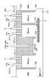
図1および図2に示されているように、リアクタ200は、円筒状の気密容器である処理容器203を備えている。処理容器203は、例えばステンレス(SUS)やアルミ合金等で構成されている。処理容器203内には、基板Sを処理する処理室201が構成されている。処理容器203にはゲートバルブ205が接続されており、ゲートバルブ205を介して基板Sが搬入出される。
次に、図7および図8を用い、本開示の一実施形態に係る基板処理工程について説明する。図7は、本実施形態に係る基板処理工程を示すフロー図である。図8は、本実施形態に係る成膜工程を示すフロー図である。以下の説明において、基板処理装置10のリアクタ200の構成各部の動作は、コントローラ300により制御される。
上述の実施形態によれば、以下に示す1つまたは複数の効果が得られる。
(b)パージ領域において、基板Sを、圧力差のある(真空度の異なる)複数の領域を通過させることにより、高いアスペクト比の溝内の副生成物を除去し、パーティクルの発生を抑制することが可能となる。
(c)パージ領域において、圧力の低い(高真空の)領域における移動距離を長くすることにより、基板S上の副生成物をより効果的に除去することができる。
(d)パージ領域において、圧力の低い(高真空の)領域に連通される排気路に接続される排気配管の内径を、他の領域に連通される排気路に接続される排気配管の内径よりも大きくすることにより、真空引きしやすくして、基板S上の副生成物を排出させやすくすることができる。
(e)パージ領域において、圧力の低い(高真空の)領域に連通される排気路に連通される排気配管に補助ポンプを設けることにより、真空ポンプのみ設けた場合と比較して、真空引きしやすくして、基板S上の副生成物を排出させやすくすることができる。
パージ領域207a,207bを構成する天井の形状等は、上述した実施形態に示す態様に限定されない。例えば、以下に示す実施形態のように変更することも可能である。以下では、主に、上述した実施形態と異なる箇所について記載する。以下の実施形態によっても、上述の実施形態に示す態様と同様の効果が得られる。
図9は、上述した図1に示すリアクタ200のB-B'線断面図の変形例である。本変形例では、パージ領域207a,207bにおける第2領域が異なる。ここでは、パージ領域207aを用いて説明する。
図10は、上述した図1に示すリアクタ200のB-B'線断面図の変形例である。本変形例では、パージ領域207a,207bが、それぞれ4つの領域に区画されている。ここでは、パージ領域207aを用いて説明する。
以下に、本開示の好ましい態様について付記する。
(付記1)
基板を処理する処理室と、
前記処理室内に設けられ、前記基板が載置される載置部を複数有する基板支持部と、を備え、
前記処理室は、前記基板に処理ガスを供給する処理領域と、前記基板をパージするパージ領域と、を有し、
前記パージ領域は、第1の圧力でパージする第1パージ領域と、前記第1の圧力よりも高い第2の圧力でパージする第2パージ領域と、
を有する基板処理装置。
(付記2)
付記1記載の基板処理装置であって、
前記パージ領域には、前記基板支持部と対向して設けられた天井と、前記天井と連続して形成され、前記第1パージ領域と前記第2パージ領域とを仕切る仕切部と、が設けられ、
前記第1パージ領域の天井の高さは、前記第2パージ領域の天井の高さよりも低く、前記仕切部の下端位置以上の高さに構成される。
(付記3)
付記1又は付記2に記載の基板処理装置であって、
前記第1パージ領域に接続される排気配管の径は、前記第2パージ領域に接続される排気配管の径よりも大きく構成される。
(付記4)
付記2記載の基板処理装置であって、
前記処理室を構成する処理容器の天板の下面により前記天井が構成され、
前記第1パージ領域の天板の上面の高さは、前記第2パージ領域の天板の上面の高さよりも低く構成される。
(付記5)
付記1から付記4のいずれか記載の基板処理装置であって、
前記第2パージ領域における圧力は、前記処理領域における圧力よりも低く構成される。
(付記6)
付記1から付記5のいずれか記載の基板処理装置であって、
前記第1パージ領域における前記基板の移動距離は、前記第2パージ領域における前記基板の移動距離よりも長くなるよう構成される。
(付記7)
付記1から付記6のいずれか記載の基板処理装置であって、
前記パージ領域は、第3の圧力でパージする第3パージ領域をさらに有し、
前記第2パージ領域と前記第3パージ領域に、パージガスを供給するパージガス供給部と、
前記第3パージ領域における圧力が、前記処理領域における圧力よりも低く、前記第2パージ領域における圧力よりも高くなるように、前記第2パージ領域と前記第3パージ領域における排気量と、前記パージガス供給部によるパージガスの供給流量のいずれか又は両方を制御するよう構成される制御部と、
を有する。
(付記8)
基板が載置される載置部を複数有する基板支持部を備え、処理ガスを供給する処理領域と、第1の圧力でパージする第1パージ領域と、前記第1の圧力よりも高い第2の圧力でパージする第2パージ領域と、を備える処理室内で、
前記基板に対して、前記処理ガスを供給する工程と、
前記基板に対して、前記第1の圧力でパージする工程と、
前記基板に対して、前記第1の圧力の少なくとも前または後に、前記第2の圧力でパージする工程と、を有する
半導体装置の製造方法。
(付記9)
基板が載置される載置部を複数有する基板支持部を備え、処理ガスを供給する処理領域と、第1の圧力でパージする第1パージ領域と、前記第1の圧力よりも高い第2の圧力でパージする第2パージ領域と、を備える基板処理装置の処理室内で、
前記基板に対して、前記処理ガスを供給する手順と、
前記基板に対して、前記第1の圧力でパージする手順と、
前記基板に対して、前記第1の圧力の少なくとも前または後に、前記第2の圧力でパージする手順と、
をコンピュータにより前記基板処理装置に実行させるプログラム。
200 リアクタ
201 処理室
203 処理容器
206a 第1処理領域、
206b 第2処理領域、
207a,207b パージ領域
217 回転テーブル(基板支持部)
217b 凹部(載置部)
300 コントローラ(制御部)
Claims (9)
- 基板を処理する処理室と、
前記処理室内に設けられ、前記基板が載置される載置部を複数有する基板支持部と、を備え、
前記処理室は、前記基板に処理ガスを供給する処理領域と、前記基板をパージするパージ領域と、を有し、
前記パージ領域は、第1の圧力でパージする第1パージ領域と、前記第1の圧力よりも高い第2の圧力でパージする第2パージ領域と、前記基板支持部と対向し、前記第1パージ領域と前記第2パージ領域に連続して設けられる天井と、を有し、
前記第1パージ領域における前記天井の高さは、前記第2パージ領域における前記天井の高さよりも低く構成される
基板処理装置。 - 前記パージ領域には、前記天井と連続して形成され、前記第1パージ領域と前記第2パージ領域とを仕切る仕切部が設けられる請求項1に記載の基板処理装置。
- 前記第1パージ領域に接続される排気配管の径は、前記第2パージ領域に接続される排気配管の径よりも大きく構成される請求項1又は2に記載の基板処理装置。
- 前記処理室を構成する処理容器の天板の下面により前記天井が構成され、
前記第1パージ領域の天板の上面の高さは、前記第2パージ領域の天板の上面の高さよりも低く構成される請求項1又は2に記載の基板処理装置。 - 前記第2パージ領域における圧力は、前記処理領域における圧力よりも低く構成される請求項1から4のいずれか一項に記載の基板処理装置。
- 前記第1パージ領域における前記基板の移動距離は、前記第2パージ領域における前記基板の移動距離よりも長くなるよう構成される請求項1から5のいずれか一項に記載の基板処理装置。
- 前記パージ領域は、第3の圧力でパージする第3パージ領域をさらに有し、
前記第2パージ領域と前記第3パージ領域に、パージガスを供給するパージガス供給部と、
前記第3パージ領域における圧力が、前記処理領域における圧力よりも低く、前記第2パージ領域における圧力よりも高くなるように、前記第2パージ領域と前記第3パージ領域における排気量と、前記パージガス供給部によるパージガスの供給流量のいずれか又は両方を制御することが可能なよう構成される制御部と、
を有する請求項1から6のいずれか一項に記載の基板処理装置。 - 基板が載置される載置部を複数有する基板支持部を備え、処理ガスを供給する処理領域と、第1の圧力でパージする第1パージ領域と、前記第1の圧力よりも高い第2の圧力でパージする第2パージ領域と、前記基板支持部と対向し、前記第1パージ領域と前記第2パージ領域に連続して設けられる天井と、を備え、前記第1パージ領域における前記天井の高さは、前記第2パージ領域における前記天井の高さよりも低く構成される処理室内で、
前記基板に対して、前記処理ガスを供給する工程と、
前記基板に対して、前記第1の圧力でパージする工程と、
前記基板に対して、前記第1の圧力の少なくとも前または後に、前記第2の圧力でパージする工程と、
を有する半導体装置の製造方法。 - 基板が載置される載置部を複数有する基板支持部を備え、処理ガスを供給する処理領域と、第1の圧力でパージする第1パージ領域と、前記第1の圧力よりも高い第2の圧力でパージする第2パージ領域と、前記基板支持部と対向し、前記第1パージ領域と前記第2パージ領域に連続して設けられる天井と、を備え、前記第1パージ領域における前記天井の高さは、前記第2パージ領域における前記天井の高さよりも低く構成される基板処理装置の処理室内で、
前記基板に対して、前記処理ガスを供給する手順と、
前記基板に対して、前記第1の圧力でパージする手順と、
前記基板に対して、前記第1の圧力の少なくとも前または後に、前記第2の圧力でパージする手順と、
をコンピュータにより前記基板処理装置に実行させるプログラム。
Priority Applications (7)
| Application Number | Priority Date | Filing Date | Title |
|---|---|---|---|
| JP2020054334A JP7098677B2 (ja) | 2020-03-25 | 2020-03-25 | 基板処理装置、半導体装置の製造方法及びプログラム |
| KR1020200110837A KR102514775B1 (ko) | 2020-03-25 | 2020-09-01 | 기판 처리 장치, 반도체 장치의 제조 방법 및 기록 매체 |
| TW109130311A TWI839568B (zh) | 2020-03-25 | 2020-09-04 | 基板處理裝置、半導體裝置之製造方法及程式 |
| US17/012,875 US11473196B2 (en) | 2020-03-25 | 2020-09-04 | Substrate processing apparatus |
| CN202010963604.1A CN113451169B (zh) | 2020-03-25 | 2020-09-14 | 基板处理装置、半导体装置的制造方法和记录介质 |
| JP2022104996A JP7345019B2 (ja) | 2020-03-25 | 2022-06-29 | 基板処理装置、基板処理方法、プログラム及び半導体装置の製造方法 |
| US17/941,446 US11926893B2 (en) | 2020-03-25 | 2022-09-09 | Substrate processing apparatus, substrate processing method and non-transitory computer-readable recording medium therefor |
Applications Claiming Priority (1)
| Application Number | Priority Date | Filing Date | Title |
|---|---|---|---|
| JP2020054334A JP7098677B2 (ja) | 2020-03-25 | 2020-03-25 | 基板処理装置、半導体装置の製造方法及びプログラム |
Related Child Applications (1)
| Application Number | Title | Priority Date | Filing Date |
|---|---|---|---|
| JP2022104996A Division JP7345019B2 (ja) | 2020-03-25 | 2022-06-29 | 基板処理装置、基板処理方法、プログラム及び半導体装置の製造方法 |
Publications (2)
| Publication Number | Publication Date |
|---|---|
| JP2021158143A JP2021158143A (ja) | 2021-10-07 |
| JP7098677B2 true JP7098677B2 (ja) | 2022-07-11 |
Family
ID=77808614
Family Applications (2)
| Application Number | Title | Priority Date | Filing Date |
|---|---|---|---|
| JP2020054334A Active JP7098677B2 (ja) | 2020-03-25 | 2020-03-25 | 基板処理装置、半導体装置の製造方法及びプログラム |
| JP2022104996A Active JP7345019B2 (ja) | 2020-03-25 | 2022-06-29 | 基板処理装置、基板処理方法、プログラム及び半導体装置の製造方法 |
Family Applications After (1)
| Application Number | Title | Priority Date | Filing Date |
|---|---|---|---|
| JP2022104996A Active JP7345019B2 (ja) | 2020-03-25 | 2022-06-29 | 基板処理装置、基板処理方法、プログラム及び半導体装置の製造方法 |
Country Status (5)
| Country | Link |
|---|---|
| US (2) | US11473196B2 (ja) |
| JP (2) | JP7098677B2 (ja) |
| KR (1) | KR102514775B1 (ja) |
| CN (1) | CN113451169B (ja) |
| TW (1) | TWI839568B (ja) |
Families Citing this family (8)
| Publication number | Priority date | Publication date | Assignee | Title |
|---|---|---|---|---|
| JP7030858B2 (ja) * | 2020-01-06 | 2022-03-07 | 株式会社Kokusai Electric | 半導体装置の製造方法、基板処理装置およびプログラム |
| JP7098677B2 (ja) | 2020-03-25 | 2022-07-11 | 株式会社Kokusai Electric | 基板処理装置、半導体装置の製造方法及びプログラム |
| CN113984485A (zh) * | 2021-09-30 | 2022-01-28 | 深圳中科飞测科技股份有限公司 | 清洁方法及相关装置 |
| JP7440480B2 (ja) * | 2021-12-13 | 2024-02-28 | 株式会社Kokusai Electric | 基板処理装置、半導体装置の製造方法、およびプログラム |
| JP7747418B2 (ja) * | 2022-02-17 | 2025-10-01 | 東京エレクトロン株式会社 | 基板処理装置、および基板処理方法 |
| US12417890B2 (en) | 2022-10-25 | 2025-09-16 | Applied Materials, Inc. | Methods, systems, and apparatus for monitoring radiation output of lamps |
| JP2024067980A (ja) * | 2022-11-07 | 2024-05-17 | 東京エレクトロン株式会社 | 基板処理装置の制御方法及び基板処理装置 |
| WO2026069552A1 (ja) * | 2024-09-26 | 2026-04-02 | 株式会社Kokusai Electric | 基板処理方法、半導体装置の製造方法、プログラム、および基板処理装置 |
Citations (4)
| Publication number | Priority date | Publication date | Assignee | Title |
|---|---|---|---|---|
| JP2011135003A (ja) | 2009-12-25 | 2011-07-07 | Tokyo Electron Ltd | 成膜装置及び成膜方法 |
| JP2013065791A (ja) | 2011-09-20 | 2013-04-11 | Hitachi Kokusai Electric Inc | 基板処理装置及び半導体装置の製造方法 |
| JP2015181149A (ja) | 2014-03-06 | 2015-10-15 | 株式会社日立国際電気 | 基板処理装置及び半導体装置の製造方法並びに記録媒体 |
| JP2017034013A (ja) | 2015-07-30 | 2017-02-09 | 株式会社日立国際電気 | 基板処理装置、半導体装置の製造方法及びプログラム |
Family Cites Families (98)
| Publication number | Priority date | Publication date | Assignee | Title |
|---|---|---|---|---|
| JPH0666298B2 (ja) * | 1983-02-03 | 1994-08-24 | 日電アネルバ株式会社 | ドライエッチング装置 |
| US5863337A (en) * | 1993-02-16 | 1999-01-26 | Ppg Industries, Inc. | Apparatus for coating a moving glass substrate |
| US6198074B1 (en) * | 1996-09-06 | 2001-03-06 | Mattson Technology, Inc. | System and method for rapid thermal processing with transitional heater |
| US6869641B2 (en) * | 2002-07-03 | 2005-03-22 | Unaxis Balzers Ltd. | Method and apparatus for ALD on a rotary susceptor |
| US6821563B2 (en) * | 2002-10-02 | 2004-11-23 | Applied Materials, Inc. | Gas distribution system for cyclical layer deposition |
| CN100459060C (zh) * | 2003-02-05 | 2009-02-04 | 株式会社半导体能源研究所 | 显示装置的制造方法 |
| JP4233348B2 (ja) * | 2003-02-24 | 2009-03-04 | シャープ株式会社 | プラズマプロセス装置 |
| JP4219295B2 (ja) * | 2004-03-31 | 2009-02-04 | シャープ株式会社 | イオン注入装置 |
| DE102004056170A1 (de) * | 2004-08-06 | 2006-03-16 | Aixtron Ag | Vorrichtung und Verfahren zur chemischen Gasphasenabscheidung mit hohem Durchsatz |
| US20060073276A1 (en) * | 2004-10-04 | 2006-04-06 | Eric Antonissen | Multi-zone atomic layer deposition apparatus and method |
| US7236324B2 (en) * | 2005-10-18 | 2007-06-26 | Hitachi Global Storage Technologies | Apparatus, method and system for fabricating servo patterns on high density patterned media |
| US20070215036A1 (en) * | 2006-03-15 | 2007-09-20 | Hyung-Sang Park | Method and apparatus of time and space co-divided atomic layer deposition |
| US7413982B2 (en) | 2006-03-29 | 2008-08-19 | Eastman Kodak Company | Process for atomic layer deposition |
| CN102892248B (zh) * | 2006-12-28 | 2016-08-10 | 荷兰应用科学研究会(Tno) | 表面介质阻挡放电等离子体单元和产生表面等离子体的方法 |
| US11136667B2 (en) | 2007-01-08 | 2021-10-05 | Eastman Kodak Company | Deposition system and method using a delivery head separated from a substrate by gas pressure |
| US8039052B2 (en) * | 2007-09-06 | 2011-10-18 | Intermolecular, Inc. | Multi-region processing system and heads |
| US8398770B2 (en) * | 2007-09-26 | 2013-03-19 | Eastman Kodak Company | Deposition system for thin film formation |
| US7851380B2 (en) * | 2007-09-26 | 2010-12-14 | Eastman Kodak Company | Process for atomic layer deposition |
| US8182608B2 (en) * | 2007-09-26 | 2012-05-22 | Eastman Kodak Company | Deposition system for thin film formation |
| US8211231B2 (en) * | 2007-09-26 | 2012-07-03 | Eastman Kodak Company | Delivery device for deposition |
| US8282735B2 (en) * | 2007-11-27 | 2012-10-09 | Asm Genitech Korea Ltd. | Atomic layer deposition apparatus |
| KR100949913B1 (ko) * | 2007-11-28 | 2010-03-30 | 주식회사 케이씨텍 | 원자층 증착 장치 |
| US8273178B2 (en) * | 2008-02-28 | 2012-09-25 | Asm Genitech Korea Ltd. | Thin film deposition apparatus and method of maintaining the same |
| JP5310283B2 (ja) * | 2008-06-27 | 2013-10-09 | 東京エレクトロン株式会社 | 成膜方法、成膜装置、基板処理装置及び記憶媒体 |
| US20100226629A1 (en) * | 2008-07-21 | 2010-09-09 | Solopower, Inc. | Roll-to-roll processing and tools for thin film solar cell manufacturing |
| US8470718B2 (en) * | 2008-08-13 | 2013-06-25 | Synos Technology, Inc. | Vapor deposition reactor for forming thin film |
| EP2159304A1 (en) * | 2008-08-27 | 2010-03-03 | Nederlandse Organisatie voor toegepast- natuurwetenschappelijk onderzoek TNO | Apparatus and method for atomic layer deposition |
| JP5276388B2 (ja) * | 2008-09-04 | 2013-08-28 | 東京エレクトロン株式会社 | 成膜装置及び基板処理装置 |
| JP5107185B2 (ja) * | 2008-09-04 | 2012-12-26 | 東京エレクトロン株式会社 | 成膜装置、基板処理装置、成膜方法及びこの成膜方法を実行させるためのプログラムを記録した記録媒体 |
| JP5276387B2 (ja) * | 2008-09-04 | 2013-08-28 | 東京エレクトロン株式会社 | 成膜装置、基板処理装置、成膜方法及びこの成膜方法を実行させるためのプログラムを記録した記録媒体 |
| JP5445044B2 (ja) * | 2008-11-14 | 2014-03-19 | 東京エレクトロン株式会社 | 成膜装置 |
| KR101021372B1 (ko) * | 2008-12-29 | 2011-03-14 | 주식회사 케이씨텍 | 원자층 증착장치 |
| EP2281921A1 (en) * | 2009-07-30 | 2011-02-09 | Nederlandse Organisatie voor toegepast -natuurwetenschappelijk onderzoek TNO | Apparatus and method for atomic layer deposition. |
| JP5648349B2 (ja) * | 2009-09-17 | 2015-01-07 | 東京エレクトロン株式会社 | 成膜装置 |
| US20110097492A1 (en) * | 2009-10-27 | 2011-04-28 | Kerr Roger S | Fluid distribution manifold operating state management system |
| US20110097494A1 (en) * | 2009-10-27 | 2011-04-28 | Kerr Roger S | Fluid conveyance system including flexible retaining mechanism |
| JP5553588B2 (ja) * | 2009-12-10 | 2014-07-16 | 東京エレクトロン株式会社 | 成膜装置 |
| KR20110077743A (ko) * | 2009-12-30 | 2011-07-07 | 주식회사 케이씨텍 | 다성분 박막의 증착을 위한 원자층 증착장치 |
| KR101171677B1 (ko) * | 2009-12-31 | 2012-08-09 | 주식회사 케이씨텍 | 다성분 박막의 증착을 위한 원자층 증착장치 |
| EP2360293A1 (en) * | 2010-02-11 | 2011-08-24 | Nederlandse Organisatie voor toegepast -natuurwetenschappelijk onderzoek TNO | Method and apparatus for depositing atomic layers on a substrate |
| EP2362002A1 (en) * | 2010-02-18 | 2011-08-31 | Nederlandse Organisatie voor toegepast -natuurwetenschappelijk onderzoek TNO | Continuous patterned layer deposition |
| EP2362001A1 (en) * | 2010-02-25 | 2011-08-31 | Nederlandse Organisatie voor toegepast -natuurwetenschappelijk onderzoek TNO | Method and device for layer deposition |
| EP2362411A1 (en) * | 2010-02-26 | 2011-08-31 | Nederlandse Organisatie voor toegepast -natuurwetenschappelijk onderzoek TNO | Apparatus and method for reactive ion etching |
| JP5812606B2 (ja) * | 2010-02-26 | 2015-11-17 | 株式会社日立国際電気 | 基板処理装置及び半導体装置の製造方法 |
| JP5444044B2 (ja) * | 2010-03-02 | 2014-03-19 | 東京エレクトロン株式会社 | プラズマ処理装置及びシャワーヘッド |
| EP2441860A1 (en) * | 2010-10-13 | 2012-04-18 | Nederlandse Organisatie voor toegepast -natuurwetenschappelijk onderzoek TNO | Apparatus and method for atomic layer deposition on a surface |
| KR101246170B1 (ko) | 2011-01-13 | 2013-03-25 | 국제엘렉트릭코리아 주식회사 | 반도체 제조에 사용되는 분사부재 및 그것을 갖는 플라즈마 처리 장치 |
| EP2481830A1 (en) * | 2011-01-31 | 2012-08-01 | Nederlandse Organisatie voor toegepast -natuurwetenschappelijk onderzoek TNO | Apparatus for atomic layer deposition. |
| EP2481832A1 (en) * | 2011-01-31 | 2012-08-01 | Nederlandse Organisatie voor toegepast -natuurwetenschappelijk onderzoek TNO | Apparatus for atomic layer deposition |
| US8143147B1 (en) * | 2011-02-10 | 2012-03-27 | Intermolecular, Inc. | Methods and systems for forming thin films |
| US20120222620A1 (en) * | 2011-03-01 | 2012-09-06 | Applied Materials, Inc. | Atomic Layer Deposition Carousel with Continuous Rotation and Methods of Use |
| US20120225191A1 (en) * | 2011-03-01 | 2012-09-06 | Applied Materials, Inc. | Apparatus and Process for Atomic Layer Deposition |
| EP2557198A1 (en) * | 2011-08-10 | 2013-02-13 | Nederlandse Organisatie voor toegepast -natuurwetenschappelijk onderzoek TNO | Method and apparatus for depositing atomic layers on a substrate |
| KR101318174B1 (ko) * | 2011-08-23 | 2013-10-18 | 주식회사 에스에프에이 | 서셉터 및 이를 구비하는 화학기상증착장치 |
| US8633115B2 (en) * | 2011-11-30 | 2014-01-21 | Applied Materials, Inc. | Methods for atomic layer etching |
| US9598766B2 (en) * | 2012-05-27 | 2017-03-21 | Air Products And Chemicals, Inc. | Vessel with filter |
| KR102002042B1 (ko) * | 2012-05-29 | 2019-07-19 | 주성엔지니어링(주) | 기판 처리 장치 및 기판 처리 방법 |
| KR20130142869A (ko) * | 2012-06-20 | 2013-12-30 | 주식회사 엠티에스나노테크 | 원자층 증착 장치 및 방법 |
| KR101397162B1 (ko) * | 2012-08-23 | 2014-05-19 | 주성엔지니어링(주) | 기판 처리 장치 및 기판 처리 방법 |
| US8973524B2 (en) * | 2012-11-27 | 2015-03-10 | Intermolecular, Inc. | Combinatorial spin deposition |
| JP5956972B2 (ja) * | 2012-12-21 | 2016-07-27 | 東京エレクトロン株式会社 | 成膜方法 |
| JP5913079B2 (ja) * | 2012-12-21 | 2016-04-27 | 東京エレクトロン株式会社 | 成膜方法 |
| EP2765218A1 (en) * | 2013-02-07 | 2014-08-13 | Nederlandse Organisatie voor toegepast-natuurwetenschappelijk Onderzoek TNO | Method and apparatus for depositing atomic layers on a substrate |
| TWI624560B (zh) * | 2013-02-18 | 2018-05-21 | 應用材料股份有限公司 | 用於原子層沉積的氣體分配板及原子層沉積系統 |
| KR101301471B1 (ko) * | 2013-03-26 | 2013-09-10 | (주)대흥정밀산업 | 챔버타입의 원자층 고속 증착장치 |
| TWI722978B (zh) * | 2013-04-16 | 2021-04-01 | 美商應用材料股份有限公司 | 用於原子層沉積之加熱燈 |
| KR102115337B1 (ko) * | 2013-07-31 | 2020-05-26 | 주성엔지니어링(주) | 기판 처리 장치 |
| JP6529973B2 (ja) * | 2013-11-26 | 2019-06-12 | アプライド マテリアルズ インコーポレイテッドApplied Materials,Incorporated | バッチ処理用傾斜プレート及びその使用方法 |
| JP6692754B2 (ja) * | 2014-01-13 | 2020-05-13 | アプライド マテリアルズ インコーポレイテッドApplied Materials,Incorporated | 空間的原子層堆積法による、自己整合ダブルパターニング |
| JP5800952B1 (ja) * | 2014-04-24 | 2015-10-28 | 株式会社日立国際電気 | 基板処理装置、半導体装置の製造方法、プログラム及び記録媒体 |
| JP6225842B2 (ja) * | 2014-06-16 | 2017-11-08 | 東京エレクトロン株式会社 | 成膜装置、成膜方法、記憶媒体 |
| EP2957656A1 (en) * | 2014-06-20 | 2015-12-23 | Nederlandse Organisatie voor toegepast- natuurwetenschappelijk onderzoek TNO | Method and apparatus for depositing atomic layers on a substrate |
| EP2960358A1 (en) * | 2014-06-25 | 2015-12-30 | Nederlandse Organisatie voor toegepast- natuurwetenschappelijk onderzoek TNO | Plasma source and surface treatment method |
| US10196741B2 (en) * | 2014-06-27 | 2019-02-05 | Applied Materials, Inc. | Wafer placement and gap control optimization through in situ feedback |
| US9837254B2 (en) * | 2014-08-12 | 2017-12-05 | Lam Research Corporation | Differentially pumped reactive gas injector |
| JP6298383B2 (ja) * | 2014-08-19 | 2018-03-20 | 株式会社日立国際電気 | 基板処理装置及び半導体装置の製造方法 |
| KR102297567B1 (ko) * | 2014-09-01 | 2021-09-02 | 삼성전자주식회사 | 가스 주입 장치 및 이를 포함하는 박막 증착 장비 |
| US20160068961A1 (en) * | 2014-09-05 | 2016-03-10 | Aixtron Se | Method and Apparatus For Growing Binary, Ternary and Quaternary Materials on a Substrate |
| TWI696724B (zh) * | 2014-09-10 | 2020-06-21 | 美商應用材料股份有限公司 | 空間原子層沈積中的氣體分離控制 |
| JP5800972B1 (ja) * | 2014-09-10 | 2015-10-28 | 株式会社日立国際電気 | 基板処理装置、半導体装置の製造方法、ガス供給ユニット、カートリッジヘッド及びプログラム |
| JP6305314B2 (ja) * | 2014-10-29 | 2018-04-04 | 東京エレクトロン株式会社 | 成膜装置およびシャワーヘッド |
| TWI676709B (zh) * | 2015-01-22 | 2019-11-11 | 美商應用材料股份有限公司 | 使用空間上分開的佈植器腔室進行的對薄膜的原子層沈積 |
| WO2016122835A1 (en) * | 2015-01-30 | 2016-08-04 | Applied Materials, Inc. | Lamp heating for process chamber |
| JP6388553B2 (ja) * | 2015-03-03 | 2018-09-12 | 東京エレクトロン株式会社 | 基板処理装置及び基板処理方法 |
| TWI723997B (zh) * | 2015-06-19 | 2021-04-11 | 美商應用材料股份有限公司 | 用於批次處理之注射器及使用方法 |
| US10550469B2 (en) * | 2015-09-04 | 2020-02-04 | Lam Research Corporation | Plasma excitation for spatial atomic layer deposition (ALD) reactors |
| WO2017048911A1 (en) * | 2015-09-19 | 2017-03-23 | Applied Materials, Inc. | Surface-selective atomic layer deposition using hydrosilylation passivation |
| KR102462931B1 (ko) * | 2015-10-30 | 2022-11-04 | 삼성전자주식회사 | 가스 공급 유닛 및 기판 처리 장치 |
| US10364497B2 (en) | 2016-02-11 | 2019-07-30 | Intermolecular, Inc. | Vapor based site-isolated processing systems and methods |
| JP6538582B2 (ja) | 2016-02-15 | 2019-07-03 | 株式会社Kokusai Electric | 基板処理装置、半導体装置の製造方法およびプログラム |
| US20170247794A1 (en) * | 2016-02-25 | 2017-08-31 | Sandisk Technologies Llc | Single chamber multi-partition deposition tool and method of operating same |
| KR102483547B1 (ko) * | 2016-06-30 | 2023-01-02 | 삼성전자주식회사 | 가스 공급 유닛 및 이를 포함하는 박막 증착 장치 |
| EP3523640B1 (en) * | 2016-10-05 | 2023-01-18 | Abbott Laboratories | Devices for sample analysis |
| US10400332B2 (en) * | 2017-03-14 | 2019-09-03 | Eastman Kodak Company | Deposition system with interlocking deposition heads |
| US10537031B2 (en) * | 2017-03-22 | 2020-01-14 | Service Support Specialties, Inc. | Reflow soldering apparatus, system and method |
| JP6971887B2 (ja) * | 2018-03-02 | 2021-11-24 | 東京エレクトロン株式会社 | 成膜方法及び成膜装置 |
| US11174553B2 (en) * | 2018-06-18 | 2021-11-16 | Applied Materials, Inc. | Gas distribution assembly for improved pump-purge and precursor delivery |
| JP7098677B2 (ja) * | 2020-03-25 | 2022-07-11 | 株式会社Kokusai Electric | 基板処理装置、半導体装置の製造方法及びプログラム |
-
2020
- 2020-03-25 JP JP2020054334A patent/JP7098677B2/ja active Active
- 2020-09-01 KR KR1020200110837A patent/KR102514775B1/ko active Active
- 2020-09-04 TW TW109130311A patent/TWI839568B/zh active
- 2020-09-04 US US17/012,875 patent/US11473196B2/en active Active
- 2020-09-14 CN CN202010963604.1A patent/CN113451169B/zh active Active
-
2022
- 2022-06-29 JP JP2022104996A patent/JP7345019B2/ja active Active
- 2022-09-09 US US17/941,446 patent/US11926893B2/en active Active
Patent Citations (4)
| Publication number | Priority date | Publication date | Assignee | Title |
|---|---|---|---|---|
| JP2011135003A (ja) | 2009-12-25 | 2011-07-07 | Tokyo Electron Ltd | 成膜装置及び成膜方法 |
| JP2013065791A (ja) | 2011-09-20 | 2013-04-11 | Hitachi Kokusai Electric Inc | 基板処理装置及び半導体装置の製造方法 |
| JP2015181149A (ja) | 2014-03-06 | 2015-10-15 | 株式会社日立国際電気 | 基板処理装置及び半導体装置の製造方法並びに記録媒体 |
| JP2017034013A (ja) | 2015-07-30 | 2017-02-09 | 株式会社日立国際電気 | 基板処理装置、半導体装置の製造方法及びプログラム |
Also Published As
| Publication number | Publication date |
|---|---|
| KR102514775B1 (ko) | 2023-03-27 |
| CN113451169A (zh) | 2021-09-28 |
| US11926893B2 (en) | 2024-03-12 |
| KR20210119860A (ko) | 2021-10-06 |
| JP2022132676A (ja) | 2022-09-09 |
| US20230002892A1 (en) | 2023-01-05 |
| CN113451169B (zh) | 2024-02-06 |
| JP7345019B2 (ja) | 2023-09-14 |
| JP2021158143A (ja) | 2021-10-07 |
| US11473196B2 (en) | 2022-10-18 |
| TWI839568B (zh) | 2024-04-21 |
| TW202137362A (zh) | 2021-10-01 |
| US20210301397A1 (en) | 2021-09-30 |
Similar Documents
| Publication | Publication Date | Title |
|---|---|---|
| JP7098677B2 (ja) | 基板処理装置、半導体装置の製造方法及びプログラム | |
| US10590534B2 (en) | Film deposition method and film deposition apparatus | |
| TW201611158A (zh) | 基板處理裝置,半導體裝置之製造方法及基板處理方法 | |
| JP6995073B2 (ja) | 基板処理装置及び半導体装置の製造方法、プログラム | |
| US20230073084A1 (en) | Substrate processing apparatus, substrate processing method and non-transitory computer-readable recording medium | |
| JP7102478B2 (ja) | 基板処理装置、半導体装置の製造方法、プログラム及び基板処理方法 | |
| KR102918593B1 (ko) | 반도체 장치의 제조 방법, 기판 처리 방법, 기판 처리 장치 및 프로그램 | |
| JP7037526B2 (ja) | 基板処理装置、半導体装置の製造方法及びプログラム | |
| JP7250085B2 (ja) | 基板処理装置、半導体装置の製造方法及びプログラム |
Legal Events
| Date | Code | Title | Description |
|---|---|---|---|
| RD03 | Notification of appointment of power of attorney |
Free format text: JAPANESE INTERMEDIATE CODE: A7423 Effective date: 20201102 |
|
| A521 | Request for written amendment filed |
Free format text: JAPANESE INTERMEDIATE CODE: A523 Effective date: 20210318 |
|
| A621 | Written request for application examination |
Free format text: JAPANESE INTERMEDIATE CODE: A621 Effective date: 20210318 |
|
| A977 | Report on retrieval |
Free format text: JAPANESE INTERMEDIATE CODE: A971007 Effective date: 20220131 |
|
| A131 | Notification of reasons for refusal |
Free format text: JAPANESE INTERMEDIATE CODE: A131 Effective date: 20220208 |
|
| A521 | Request for written amendment filed |
Free format text: JAPANESE INTERMEDIATE CODE: A523 Effective date: 20220406 |
|
| TRDD | Decision of grant or rejection written | ||
| A01 | Written decision to grant a patent or to grant a registration (utility model) |
Free format text: JAPANESE INTERMEDIATE CODE: A01 Effective date: 20220531 |
|
| A61 | First payment of annual fees (during grant procedure) |
Free format text: JAPANESE INTERMEDIATE CODE: A61 Effective date: 20220629 |
|
| R150 | Certificate of patent or registration of utility model |
Ref document number: 7098677 Country of ref document: JP Free format text: JAPANESE INTERMEDIATE CODE: R150 |
|
| R250 | Receipt of annual fees |
Free format text: JAPANESE INTERMEDIATE CODE: R250 |