JP7054642B2 - プラズマ処理装置及びプラズマ処理方法 - Google Patents
プラズマ処理装置及びプラズマ処理方法 Download PDFInfo
- Publication number
- JP7054642B2 JP7054642B2 JP2018073872A JP2018073872A JP7054642B2 JP 7054642 B2 JP7054642 B2 JP 7054642B2 JP 2018073872 A JP2018073872 A JP 2018073872A JP 2018073872 A JP2018073872 A JP 2018073872A JP 7054642 B2 JP7054642 B2 JP 7054642B2
- Authority
- JP
- Japan
- Prior art keywords
- electrostatic chuck
- plasma processing
- temperature
- voltage
- heat transfer
- Prior art date
- Legal status (The legal status is an assumption and is not a legal conclusion. Google has not performed a legal analysis and makes no representation as to the accuracy of the status listed.)
- Active
Links
Images


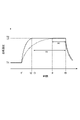

Classifications
-
- H—ELECTRICITY
- H01—ELECTRIC ELEMENTS
- H01J—ELECTRIC DISCHARGE TUBES OR DISCHARGE LAMPS
- H01J37/00—Discharge tubes with provision for introducing objects or material to be exposed to the discharge, e.g. for the purpose of examination or processing thereof
- H01J37/32—Gas-filled discharge tubes
- H01J37/32009—Arrangements for generation of plasma specially adapted for examination or treatment of objects, e.g. plasma sources
- H01J37/32082—Radio frequency generated discharge
- H01J37/32091—Radio frequency generated discharge the radio frequency energy being capacitively coupled to the plasma
-
- H—ELECTRICITY
- H01—ELECTRIC ELEMENTS
- H01J—ELECTRIC DISCHARGE TUBES OR DISCHARGE LAMPS
- H01J37/00—Discharge tubes with provision for introducing objects or material to be exposed to the discharge, e.g. for the purpose of examination or processing thereof
- H01J37/32—Gas-filled discharge tubes
- H01J37/32009—Arrangements for generation of plasma specially adapted for examination or treatment of objects, e.g. plasma sources
- H01J37/32082—Radio frequency generated discharge
- H01J37/32174—Circuits specially adapted for controlling the RF discharge
-
- H—ELECTRICITY
- H01—ELECTRIC ELEMENTS
- H01J—ELECTRIC DISCHARGE TUBES OR DISCHARGE LAMPS
- H01J37/00—Discharge tubes with provision for introducing objects or material to be exposed to the discharge, e.g. for the purpose of examination or processing thereof
- H01J37/32—Gas-filled discharge tubes
- H01J37/32431—Constructional details of the reactor
- H01J37/3244—Gas supply means
- H01J37/32449—Gas control, e.g. control of the gas flow
-
- H—ELECTRICITY
- H01—ELECTRIC ELEMENTS
- H01J—ELECTRIC DISCHARGE TUBES OR DISCHARGE LAMPS
- H01J37/00—Discharge tubes with provision for introducing objects or material to be exposed to the discharge, e.g. for the purpose of examination or processing thereof
- H01J37/32—Gas-filled discharge tubes
- H01J37/32431—Constructional details of the reactor
- H01J37/32697—Electrostatic control
-
- H—ELECTRICITY
- H01—ELECTRIC ELEMENTS
- H01J—ELECTRIC DISCHARGE TUBES OR DISCHARGE LAMPS
- H01J37/00—Discharge tubes with provision for introducing objects or material to be exposed to the discharge, e.g. for the purpose of examination or processing thereof
- H01J37/32—Gas-filled discharge tubes
- H01J37/32431—Constructional details of the reactor
- H01J37/32715—Workpiece holder
- H01J37/32724—Temperature
-
- H—ELECTRICITY
- H10—SEMICONDUCTOR DEVICES; ELECTRIC SOLID-STATE DEVICES NOT OTHERWISE PROVIDED FOR
- H10P—GENERIC PROCESSES OR APPARATUS FOR THE MANUFACTURE OR TREATMENT OF DEVICES COVERED BY CLASS H10
- H10P72/00—Handling or holding of wafers, substrates or devices during manufacture or treatment thereof
- H10P72/04—Apparatus for manufacture or treatment
- H10P72/0431—Apparatus for thermal treatment
- H10P72/0434—Apparatus for thermal treatment mainly by convection
-
- H—ELECTRICITY
- H10—SEMICONDUCTOR DEVICES; ELECTRIC SOLID-STATE DEVICES NOT OTHERWISE PROVIDED FOR
- H10P—GENERIC PROCESSES OR APPARATUS FOR THE MANUFACTURE OR TREATMENT OF DEVICES COVERED BY CLASS H10
- H10P72/00—Handling or holding of wafers, substrates or devices during manufacture or treatment thereof
- H10P72/06—Apparatus for monitoring, sorting, marking, testing or measuring
- H10P72/0602—Temperature monitoring
-
- H—ELECTRICITY
- H10—SEMICONDUCTOR DEVICES; ELECTRIC SOLID-STATE DEVICES NOT OTHERWISE PROVIDED FOR
- H10P—GENERIC PROCESSES OR APPARATUS FOR THE MANUFACTURE OR TREATMENT OF DEVICES COVERED BY CLASS H10
- H10P72/00—Handling or holding of wafers, substrates or devices during manufacture or treatment thereof
- H10P72/70—Handling or holding of wafers, substrates or devices during manufacture or treatment thereof for supporting or gripping
- H10P72/72—Handling or holding of wafers, substrates or devices during manufacture or treatment thereof for supporting or gripping using electrostatic chucks
- H10P72/722—Details of electrostatic chucks
-
- H—ELECTRICITY
- H01—ELECTRIC ELEMENTS
- H01J—ELECTRIC DISCHARGE TUBES OR DISCHARGE LAMPS
- H01J2237/00—Discharge tubes exposing object to beam, e.g. for analysis treatment, etching, imaging
- H01J2237/002—Cooling arrangements
-
- H—ELECTRICITY
- H01—ELECTRIC ELEMENTS
- H01J—ELECTRIC DISCHARGE TUBES OR DISCHARGE LAMPS
- H01J2237/00—Discharge tubes exposing object to beam, e.g. for analysis treatment, etching, imaging
- H01J2237/245—Detection characterised by the variable being measured
- H01J2237/24571—Measurements of non-electric or non-magnetic variables
- H01J2237/24585—Other variables, e.g. energy, mass, velocity, time, temperature
-
- H—ELECTRICITY
- H01—ELECTRIC ELEMENTS
- H01J—ELECTRIC DISCHARGE TUBES OR DISCHARGE LAMPS
- H01J37/00—Discharge tubes with provision for introducing objects or material to be exposed to the discharge, e.g. for the purpose of examination or processing thereof
- H01J37/32—Gas-filled discharge tubes
- H01J37/32431—Constructional details of the reactor
- H01J37/32623—Mechanical discharge control means
- H01J37/32642—Focus rings
Landscapes
- Physics & Mathematics (AREA)
- Engineering & Computer Science (AREA)
- Plasma & Fusion (AREA)
- Chemical & Material Sciences (AREA)
- Analytical Chemistry (AREA)
- Container, Conveyance, Adherence, Positioning, Of Wafer (AREA)
- Drying Of Semiconductors (AREA)
- Plasma Technology (AREA)
Priority Applications (4)
| Application Number | Priority Date | Filing Date | Title |
|---|---|---|---|
| JP2018073872A JP7054642B2 (ja) | 2018-04-06 | 2018-04-06 | プラズマ処理装置及びプラズマ処理方法 |
| KR1020190039562A KR102679358B1 (ko) | 2018-04-06 | 2019-04-04 | 플라즈마 처리 장치 및 플라즈마 처리 방법 |
| US16/375,917 US11875977B2 (en) | 2018-04-06 | 2019-04-05 | Plasma processing apparatus and plasma processing method |
| US18/538,165 US12626893B2 (en) | 2018-04-06 | 2023-12-13 | Plasma processing apparatus and plasma processing method |
Applications Claiming Priority (1)
| Application Number | Priority Date | Filing Date | Title |
|---|---|---|---|
| JP2018073872A JP7054642B2 (ja) | 2018-04-06 | 2018-04-06 | プラズマ処理装置及びプラズマ処理方法 |
Publications (3)
| Publication Number | Publication Date |
|---|---|
| JP2019186334A JP2019186334A (ja) | 2019-10-24 |
| JP2019186334A5 JP2019186334A5 (enExample) | 2021-03-11 |
| JP7054642B2 true JP7054642B2 (ja) | 2022-04-14 |
Family
ID=68096120
Family Applications (1)
| Application Number | Title | Priority Date | Filing Date |
|---|---|---|---|
| JP2018073872A Active JP7054642B2 (ja) | 2018-04-06 | 2018-04-06 | プラズマ処理装置及びプラズマ処理方法 |
Country Status (3)
| Country | Link |
|---|---|
| US (2) | US11875977B2 (enExample) |
| JP (1) | JP7054642B2 (enExample) |
| KR (1) | KR102679358B1 (enExample) |
Families Citing this family (8)
| Publication number | Priority date | Publication date | Assignee | Title |
|---|---|---|---|---|
| JP7519768B2 (ja) * | 2019-10-28 | 2024-07-22 | 東京エレクトロン株式会社 | 吸着方法、載置台及びプラズマ処理装置 |
| US11270903B2 (en) * | 2019-12-17 | 2022-03-08 | Applied Materials, Inc. | Multi zone electrostatic chuck |
| CN113130279B (zh) * | 2019-12-30 | 2023-09-29 | 中微半导体设备(上海)股份有限公司 | 下电极组件、等离子体处理装置及其工作方法 |
| JP7516198B2 (ja) * | 2020-05-01 | 2024-07-16 | 東京エレクトロン株式会社 | エッチング装置及びエッチング方法 |
| CN112466732B (zh) * | 2020-11-25 | 2024-06-21 | 北京北方华创微电子装备有限公司 | 半导体工艺设备和等离子体启辉方法 |
| JP7588518B2 (ja) * | 2021-02-01 | 2024-11-22 | 東京エレクトロン株式会社 | 温度制御方法及び基板処理装置 |
| US12062565B2 (en) * | 2021-06-29 | 2024-08-13 | Asm Ip Holding B.V. | Electrostatic chuck, assembly including the electrostatic chuck, and method of controlling temperature of the electrostatic chuck |
| CN115036202B (zh) * | 2022-06-29 | 2025-08-26 | 北京北方华创微电子装备有限公司 | 一种下射频电源的电压控制方法及半导体工艺设备 |
Citations (3)
| Publication number | Priority date | Publication date | Assignee | Title |
|---|---|---|---|---|
| JP2008034669A (ja) | 2006-07-31 | 2008-02-14 | Hitachi High-Technologies Corp | プラズマ処理装置およびプラズマ処理方法 |
| JP2011198838A (ja) | 2010-03-17 | 2011-10-06 | Tokyo Electron Ltd | 基板脱着方法 |
| JP2014011215A (ja) | 2012-06-28 | 2014-01-20 | Hitachi High-Technologies Corp | プラズマ処理装置およびプラズマ処理方法 |
Family Cites Families (15)
| Publication number | Priority date | Publication date | Assignee | Title |
|---|---|---|---|---|
| JPH07263412A (ja) * | 1994-03-18 | 1995-10-13 | Hitachi Ltd | プラズマ処理装置 |
| JP3733448B2 (ja) * | 1994-04-27 | 2006-01-11 | キヤノンアネルバ株式会社 | プラズマ処理方法および装置並びに基板脱離方法及び印加電圧の制御装置 |
| JP3208044B2 (ja) * | 1995-06-07 | 2001-09-10 | 東京エレクトロン株式会社 | プラズマ処理装置及びプラズマ処理方法 |
| JPH1014266A (ja) * | 1996-06-21 | 1998-01-16 | Sony Corp | 静電チャック装置及び静電チャックを用いたウエハの保持方法及び静電チャックからのウエハの脱着方法 |
| JPH1027780A (ja) * | 1996-07-10 | 1998-01-27 | Nec Corp | プラズマ処理方法 |
| JP3792865B2 (ja) * | 1997-10-30 | 2006-07-05 | 松下電器産業株式会社 | 半導体装置の製造装置およびドライエッチング方法 |
| JP2000049216A (ja) * | 1998-07-28 | 2000-02-18 | Mitsubishi Electric Corp | プラズマ処理装置および当該装置で用いられる静電チャック吸着方法 |
| JP2001308065A (ja) * | 2000-04-19 | 2001-11-02 | Nec Corp | ドライエッチング装置およびドライエッチング方法 |
| CN1249777C (zh) * | 2001-08-27 | 2006-04-05 | 松下电器产业株式会社 | 等离子体处理装置及等离子体处理方法 |
| US7208067B2 (en) * | 2003-03-27 | 2007-04-24 | Tokyo Electron Limited | Method and system for monitoring RF impedance to determine conditions of a wafer on an electrostatic chuck |
| JP4657949B2 (ja) * | 2006-03-01 | 2011-03-23 | 株式会社日立ハイテクノロジーズ | エッチング処理装置および自己バイアス電圧測定方法ならびにエッチング処理装置の監視方法 |
| JP5372419B2 (ja) * | 2008-06-25 | 2013-12-18 | 株式会社日立ハイテクノロジーズ | プラズマ処理装置及びプラズマ処理方法 |
| US8313664B2 (en) * | 2008-11-21 | 2012-11-20 | Applied Materials, Inc. | Efficient and accurate method for real-time prediction of the self-bias voltage of a wafer and feedback control of ESC voltage in plasma processing chamber |
| KR102168064B1 (ko) * | 2013-02-20 | 2020-10-20 | 도쿄엘렉트론가부시키가이샤 | 플라즈마 처리 장치 및 플라즈마 처리 방법 |
| US20170278730A1 (en) * | 2016-03-28 | 2017-09-28 | Hitachi High-Technologies Corporation | Plasma processing apparatus and plasma processing method |
-
2018
- 2018-04-06 JP JP2018073872A patent/JP7054642B2/ja active Active
-
2019
- 2019-04-04 KR KR1020190039562A patent/KR102679358B1/ko active Active
- 2019-04-05 US US16/375,917 patent/US11875977B2/en active Active
-
2023
- 2023-12-13 US US18/538,165 patent/US12626893B2/en active Active
Patent Citations (3)
| Publication number | Priority date | Publication date | Assignee | Title |
|---|---|---|---|---|
| JP2008034669A (ja) | 2006-07-31 | 2008-02-14 | Hitachi High-Technologies Corp | プラズマ処理装置およびプラズマ処理方法 |
| JP2011198838A (ja) | 2010-03-17 | 2011-10-06 | Tokyo Electron Ltd | 基板脱着方法 |
| JP2014011215A (ja) | 2012-06-28 | 2014-01-20 | Hitachi High-Technologies Corp | プラズマ処理装置およびプラズマ処理方法 |
Also Published As
| Publication number | Publication date |
|---|---|
| US12626893B2 (en) | 2026-05-12 |
| JP2019186334A (ja) | 2019-10-24 |
| KR20190117378A (ko) | 2019-10-16 |
| US20190311888A1 (en) | 2019-10-10 |
| KR102679358B1 (ko) | 2024-06-27 |
| US11875977B2 (en) | 2024-01-16 |
| US20240112895A1 (en) | 2024-04-04 |
Similar Documents
| Publication | Publication Date | Title |
|---|---|---|
| KR102679358B1 (ko) | 플라즈마 처리 장치 및 플라즈마 처리 방법 | |
| US12525439B2 (en) | Apparatus for plasma processing and method of etching | |
| TWI857215B (zh) | 基板支持器及電漿處理裝置 | |
| JP7349329B2 (ja) | プラズマ処理装置及びエッチング方法 | |
| US20230411128A1 (en) | Plasma processing apparatus and power supply control method | |
| JP7174687B2 (ja) | プラズマ処理装置及びエッチング方法 | |
| JP6556046B2 (ja) | プラズマ処理方法およびプラズマ処理装置 | |
| US12334305B2 (en) | Plasma processing apparatus | |
| US20200185193A1 (en) | Plasma processing apparatus and etching method | |
| JP7090149B2 (ja) | プラズマ処理装置及びプラズマエッチング方法 | |
| KR102863314B1 (ko) | 기판 지지 어셈블리, 플라즈마 처리 장치, 및 플라즈마 처리 방법 | |
| KR102936172B1 (ko) | 플라즈마 처리 방법 및 플라즈마 처리 장치 | |
| KR102825584B1 (ko) | 플라즈마 처리 장치 및 플라즈마 처리 방법 | |
| KR102869592B1 (ko) | 플라즈마 처리 장치 및 플라즈마 처리 방법 | |
| TW202312274A (zh) | 電漿處理裝置及電漿處理方法 | |
| JP6938746B1 (ja) | エッチング装置及びエッチング方法 | |
| JP2023043151A (ja) | プラズマ処理装置及びプラズマ処理方法 | |
| KR20250078478A (ko) | 플라즈마 처리 장치 및 에칭 방법 |
Legal Events
| Date | Code | Title | Description |
|---|---|---|---|
| A521 | Request for written amendment filed |
Free format text: JAPANESE INTERMEDIATE CODE: A523 Effective date: 20210127 |
|
| A621 | Written request for application examination |
Free format text: JAPANESE INTERMEDIATE CODE: A621 Effective date: 20210127 |
|
| A977 | Report on retrieval |
Free format text: JAPANESE INTERMEDIATE CODE: A971007 Effective date: 20211215 |
|
| A131 | Notification of reasons for refusal |
Free format text: JAPANESE INTERMEDIATE CODE: A131 Effective date: 20211221 |
|
| A521 | Request for written amendment filed |
Free format text: JAPANESE INTERMEDIATE CODE: A523 Effective date: 20220221 |
|
| TRDD | Decision of grant or rejection written | ||
| A01 | Written decision to grant a patent or to grant a registration (utility model) |
Free format text: JAPANESE INTERMEDIATE CODE: A01 Effective date: 20220308 |
|
| A61 | First payment of annual fees (during grant procedure) |
Free format text: JAPANESE INTERMEDIATE CODE: A61 Effective date: 20220404 |
|
| R150 | Certificate of patent or registration of utility model |
Ref document number: 7054642 Country of ref document: JP Free format text: JAPANESE INTERMEDIATE CODE: R150 |
|
| R250 | Receipt of annual fees |
Free format text: JAPANESE INTERMEDIATE CODE: R250 |
|
| R250 | Receipt of annual fees |
Free format text: JAPANESE INTERMEDIATE CODE: R250 |