JP7042039B2 - 高アスペクト構造からのデブリ除去 - Google Patents
高アスペクト構造からのデブリ除去 Download PDFInfo
- Publication number
- JP7042039B2 JP7042039B2 JP2017100801A JP2017100801A JP7042039B2 JP 7042039 B2 JP7042039 B2 JP 7042039B2 JP 2017100801 A JP2017100801 A JP 2017100801A JP 2017100801 A JP2017100801 A JP 2017100801A JP 7042039 B2 JP7042039 B2 JP 7042039B2
- Authority
- JP
- Japan
- Prior art keywords
- chip
- irradiation
- recovery
- spm
- measurement system
- Prior art date
- Legal status (The legal status is an assumption and is not a legal conclusion. Google has not performed a legal analysis and makes no representation as to the accuracy of the status listed.)
- Active
Links
- 238000011084 recovery Methods 0.000 claims description 235
- 238000005259 measurement Methods 0.000 claims description 213
- 239000002245 particle Substances 0.000 claims description 191
- 239000000758 substrate Substances 0.000 claims description 161
- 239000000356 contaminant Substances 0.000 claims description 160
- 239000000523 sample Substances 0.000 claims description 139
- 239000000463 material Substances 0.000 claims description 119
- 238000001228 spectrum Methods 0.000 claims description 34
- 230000004044 response Effects 0.000 claims description 29
- 238000012546 transfer Methods 0.000 claims description 18
- 238000010894 electron beam technology Methods 0.000 claims description 9
- 230000001678 irradiating effect Effects 0.000 claims description 7
- 238000012856 packing Methods 0.000 claims 1
- 238000000034 method Methods 0.000 description 121
- 238000004621 scanning probe microscopy Methods 0.000 description 102
- 239000002105 nanoparticle Substances 0.000 description 60
- 230000008569 process Effects 0.000 description 49
- 238000000576 coating method Methods 0.000 description 29
- 239000000126 substance Substances 0.000 description 27
- 238000004140 cleaning Methods 0.000 description 25
- 239000011248 coating agent Substances 0.000 description 25
- 239000000203 mixture Substances 0.000 description 21
- 230000003993 interaction Effects 0.000 description 20
- 238000012545 processing Methods 0.000 description 14
- 239000012530 fluid Substances 0.000 description 13
- 230000006399 behavior Effects 0.000 description 12
- OKTJSMMVPCPJKN-UHFFFAOYSA-N Carbon Chemical compound [C] OKTJSMMVPCPJKN-UHFFFAOYSA-N 0.000 description 11
- 108020004414 DNA Proteins 0.000 description 11
- 102000053602 DNA Human genes 0.000 description 11
- 229910052751 metal Inorganic materials 0.000 description 11
- 239000002184 metal Substances 0.000 description 11
- 239000010432 diamond Substances 0.000 description 10
- 230000007246 mechanism Effects 0.000 description 9
- 230000007547 defect Effects 0.000 description 8
- 238000001514 detection method Methods 0.000 description 8
- 238000009792 diffusion process Methods 0.000 description 8
- 230000008439 repair process Effects 0.000 description 8
- 238000013019 agitation Methods 0.000 description 7
- 230000000694 effects Effects 0.000 description 7
- 239000007789 gas Substances 0.000 description 7
- 150000002739 metals Chemical class 0.000 description 7
- 229920001343 polytetrafluoroethylene Polymers 0.000 description 7
- 239000004810 polytetrafluoroethylene Substances 0.000 description 7
- 239000007779 soft material Substances 0.000 description 7
- 239000000853 adhesive Substances 0.000 description 6
- 230000001070 adhesive effect Effects 0.000 description 6
- 238000006243 chemical reaction Methods 0.000 description 6
- 238000011109 contamination Methods 0.000 description 6
- 230000006378 damage Effects 0.000 description 6
- 230000007423 decrease Effects 0.000 description 6
- 239000002086 nanomaterial Substances 0.000 description 6
- 238000004804 winding Methods 0.000 description 6
- 102000007469 Actins Human genes 0.000 description 5
- 108010085238 Actins Proteins 0.000 description 5
- 239000004812 Fluorinated ethylene propylene Substances 0.000 description 5
- 230000009471 action Effects 0.000 description 5
- 238000005452 bending Methods 0.000 description 5
- 230000008901 benefit Effects 0.000 description 5
- 238000004422 calculation algorithm Methods 0.000 description 5
- 239000013078 crystal Substances 0.000 description 5
- 229910003460 diamond Inorganic materials 0.000 description 5
- 230000005672 electromagnetic field Effects 0.000 description 5
- 239000012634 fragment Substances 0.000 description 5
- 229920000554 ionomer Polymers 0.000 description 5
- 239000007788 liquid Substances 0.000 description 5
- 230000004048 modification Effects 0.000 description 5
- 238000012986 modification Methods 0.000 description 5
- 229920009441 perflouroethylene propylene Polymers 0.000 description 5
- 229920002477 rna polymer Polymers 0.000 description 5
- 108091028043 Nucleic acid sequence Proteins 0.000 description 4
- 238000013459 approach Methods 0.000 description 4
- 229910052799 carbon Inorganic materials 0.000 description 4
- 239000002041 carbon nanotube Substances 0.000 description 4
- 229910021393 carbon nanotube Inorganic materials 0.000 description 4
- 239000003344 environmental pollutant Substances 0.000 description 4
- 238000002474 experimental method Methods 0.000 description 4
- 238000001900 extreme ultraviolet lithography Methods 0.000 description 4
- 231100000719 pollutant Toxicity 0.000 description 4
- 238000010008 shearing Methods 0.000 description 4
- 238000013519 translation Methods 0.000 description 4
- 230000001960 triggered effect Effects 0.000 description 4
- 230000005641 tunneling Effects 0.000 description 4
- 238000004458 analytical method Methods 0.000 description 3
- 230000007613 environmental effect Effects 0.000 description 3
- 229910052739 hydrogen Inorganic materials 0.000 description 3
- 239000001257 hydrogen Substances 0.000 description 3
- 230000036961 partial effect Effects 0.000 description 3
- 238000000206 photolithography Methods 0.000 description 3
- 239000004033 plastic Substances 0.000 description 3
- 238000007790 scraping Methods 0.000 description 3
- 239000007787 solid Substances 0.000 description 3
- 239000004575 stone Substances 0.000 description 3
- YBJHBAHKTGYVGT-ZKWXMUAHSA-N (+)-Biotin Chemical compound N1C(=O)N[C@@H]2[C@H](CCCCC(=O)O)SC[C@@H]21 YBJHBAHKTGYVGT-ZKWXMUAHSA-N 0.000 description 2
- CURLTUGMZLYLDI-UHFFFAOYSA-N Carbon dioxide Chemical compound O=C=O CURLTUGMZLYLDI-UHFFFAOYSA-N 0.000 description 2
- WTDRDQBEARUVNC-UHFFFAOYSA-N L-Dopa Natural products OC(=O)C(N)CC1=CC=C(O)C(O)=C1 WTDRDQBEARUVNC-UHFFFAOYSA-N 0.000 description 2
- 101100460147 Sarcophaga bullata NEMS gene Proteins 0.000 description 2
- 238000010521 absorption reaction Methods 0.000 description 2
- 230000002411 adverse Effects 0.000 description 2
- 229910052792 caesium Inorganic materials 0.000 description 2
- CREMABGTGYGIQB-UHFFFAOYSA-N carbon carbon Chemical compound C.C CREMABGTGYGIQB-UHFFFAOYSA-N 0.000 description 2
- 239000011203 carbon fibre reinforced carbon Substances 0.000 description 2
- 210000004027 cell Anatomy 0.000 description 2
- 230000008859 change Effects 0.000 description 2
- 238000004666 chemical force microscopy Methods 0.000 description 2
- 150000001805 chlorine compounds Chemical class 0.000 description 2
- 150000001875 compounds Chemical class 0.000 description 2
- 238000012937 correction Methods 0.000 description 2
- 238000005520 cutting process Methods 0.000 description 2
- 230000001419 dependent effect Effects 0.000 description 2
- 238000013461 design Methods 0.000 description 2
- 239000003599 detergent Substances 0.000 description 2
- 238000000605 extraction Methods 0.000 description 2
- 150000002222 fluorine compounds Chemical class 0.000 description 2
- 230000006870 function Effects 0.000 description 2
- PCHJSUWPFVWCPO-UHFFFAOYSA-N gold Chemical compound [Au] PCHJSUWPFVWCPO-UHFFFAOYSA-N 0.000 description 2
- 229910021389 graphene Inorganic materials 0.000 description 2
- 229910052741 iridium Inorganic materials 0.000 description 2
- 230000000670 limiting effect Effects 0.000 description 2
- 238000012886 linear function Methods 0.000 description 2
- 238000001459 lithography Methods 0.000 description 2
- 229920002521 macromolecule Polymers 0.000 description 2
- 239000012528 membrane Substances 0.000 description 2
- QLOAVXSYZAJECW-UHFFFAOYSA-N methane;molecular fluorine Chemical compound C.FF QLOAVXSYZAJECW-UHFFFAOYSA-N 0.000 description 2
- 238000000386 microscopy Methods 0.000 description 2
- 239000002061 nanopillar Substances 0.000 description 2
- 238000005457 optimization Methods 0.000 description 2
- -1 polytetrafluoroethylene Polymers 0.000 description 2
- 108090000623 proteins and genes Proteins 0.000 description 2
- 102000004169 proteins and genes Human genes 0.000 description 2
- 238000012887 quadratic function Methods 0.000 description 2
- 230000005855 radiation Effects 0.000 description 2
- 238000000926 separation method Methods 0.000 description 2
- 230000000930 thermomechanical effect Effects 0.000 description 2
- 235000012431 wafers Nutrition 0.000 description 2
- 230000005457 Black-body radiation Effects 0.000 description 1
- ZOXJGFHDIHLPTG-UHFFFAOYSA-N Boron Chemical compound [B] ZOXJGFHDIHLPTG-UHFFFAOYSA-N 0.000 description 1
- PZNSFCLAULLKQX-UHFFFAOYSA-N Boron nitride Chemical class N#B PZNSFCLAULLKQX-UHFFFAOYSA-N 0.000 description 1
- 229920000049 Carbon (fiber) Polymers 0.000 description 1
- 241000238586 Cirripedia Species 0.000 description 1
- 241000195493 Cryptophyta Species 0.000 description 1
- WTDRDQBEARUVNC-LURJTMIESA-N L-DOPA Chemical compound OC(=O)[C@@H](N)CC1=CC=C(O)C(O)=C1 WTDRDQBEARUVNC-LURJTMIESA-N 0.000 description 1
- 241000242594 Platyhelminthes Species 0.000 description 1
- 108010090804 Streptavidin Proteins 0.000 description 1
- 238000003848 UV Light-Curing Methods 0.000 description 1
- 238000005411 Van der Waals force Methods 0.000 description 1
- 241000700605 Viruses Species 0.000 description 1
- 230000003213 activating effect Effects 0.000 description 1
- 239000012190 activator Substances 0.000 description 1
- 239000011149 active material Substances 0.000 description 1
- 230000001154 acute effect Effects 0.000 description 1
- 150000001260 acyclic compounds Chemical class 0.000 description 1
- 230000001464 adherent effect Effects 0.000 description 1
- 230000010062 adhesion mechanism Effects 0.000 description 1
- 230000004075 alteration Effects 0.000 description 1
- 229910052782 aluminium Inorganic materials 0.000 description 1
- XAGFODPZIPBFFR-UHFFFAOYSA-N aluminium Chemical compound [Al] XAGFODPZIPBFFR-UHFFFAOYSA-N 0.000 description 1
- 239000007864 aqueous solution Substances 0.000 description 1
- 230000004888 barrier function Effects 0.000 description 1
- 239000012620 biological material Substances 0.000 description 1
- 230000015572 biosynthetic process Effects 0.000 description 1
- 229960002685 biotin Drugs 0.000 description 1
- 235000020958 biotin Nutrition 0.000 description 1
- 239000011616 biotin Substances 0.000 description 1
- 229910052796 boron Inorganic materials 0.000 description 1
- TVFDJXOCXUVLDH-UHFFFAOYSA-N caesium atom Chemical compound [Cs] TVFDJXOCXUVLDH-UHFFFAOYSA-N 0.000 description 1
- 229910002092 carbon dioxide Inorganic materials 0.000 description 1
- 239000001569 carbon dioxide Substances 0.000 description 1
- 239000004917 carbon fiber Substances 0.000 description 1
- 230000015556 catabolic process Effects 0.000 description 1
- 230000005591 charge neutralization Effects 0.000 description 1
- 238000003889 chemical engineering Methods 0.000 description 1
- 230000003749 cleanliness Effects 0.000 description 1
- 230000006835 compression Effects 0.000 description 1
- 238000007906 compression Methods 0.000 description 1
- 230000008878 coupling Effects 0.000 description 1
- 238000010168 coupling process Methods 0.000 description 1
- 238000005859 coupling reaction Methods 0.000 description 1
- 230000002950 deficient Effects 0.000 description 1
- 238000006731 degradation reaction Methods 0.000 description 1
- 230000032798 delamination Effects 0.000 description 1
- 238000000151 deposition Methods 0.000 description 1
- 230000001066 destructive effect Effects 0.000 description 1
- 238000011161 development Methods 0.000 description 1
- MHUWZNTUIIFHAS-CLFAGFIQSA-N dioleoyl phosphatidic acid Chemical compound CCCCCCCC\C=C/CCCCCCCC(=O)OCC(COP(O)(O)=O)OC(=O)CCCCCCC\C=C/CCCCCCCC MHUWZNTUIIFHAS-CLFAGFIQSA-N 0.000 description 1
- 238000007598 dipping method Methods 0.000 description 1
- 238000006073 displacement reaction Methods 0.000 description 1
- 238000009510 drug design Methods 0.000 description 1
- 230000005489 elastic deformation Effects 0.000 description 1
- 230000005670 electromagnetic radiation Effects 0.000 description 1
- 230000008030 elimination Effects 0.000 description 1
- 238000003379 elimination reaction Methods 0.000 description 1
- 238000005516 engineering process Methods 0.000 description 1
- HQQADJVZYDDRJT-UHFFFAOYSA-N ethene;prop-1-ene Chemical group C=C.CC=C HQQADJVZYDDRJT-UHFFFAOYSA-N 0.000 description 1
- 229920005648 ethylene methacrylic acid copolymer Polymers 0.000 description 1
- 210000003527 eukaryotic cell Anatomy 0.000 description 1
- 230000005284 excitation Effects 0.000 description 1
- 230000001747 exhibiting effect Effects 0.000 description 1
- 230000005669 field effect Effects 0.000 description 1
- 239000000834 fixative Substances 0.000 description 1
- NBVXSUQYWXRMNV-UHFFFAOYSA-N fluoromethane Chemical compound FC NBVXSUQYWXRMNV-UHFFFAOYSA-N 0.000 description 1
- 230000014509 gene expression Effects 0.000 description 1
- 239000011521 glass Substances 0.000 description 1
- 229910052737 gold Inorganic materials 0.000 description 1
- 239000010931 gold Substances 0.000 description 1
- 239000010438 granite Substances 0.000 description 1
- 230000002209 hydrophobic effect Effects 0.000 description 1
- 238000007654 immersion Methods 0.000 description 1
- 230000006698 induction Effects 0.000 description 1
- 238000009434 installation Methods 0.000 description 1
- 230000010354 integration Effects 0.000 description 1
- 150000002500 ions Chemical class 0.000 description 1
- GKOZUEZYRPOHIO-UHFFFAOYSA-N iridium atom Chemical compound [Ir] GKOZUEZYRPOHIO-UHFFFAOYSA-N 0.000 description 1
- 230000002427 irreversible effect Effects 0.000 description 1
- 238000005184 irreversible process Methods 0.000 description 1
- 238000005304 joining Methods 0.000 description 1
- 229960004502 levodopa Drugs 0.000 description 1
- 159000000003 magnesium salts Chemical class 0.000 description 1
- 239000004579 marble Substances 0.000 description 1
- 230000000873 masking effect Effects 0.000 description 1
- 238000002844 melting Methods 0.000 description 1
- 230000008018 melting Effects 0.000 description 1
- 239000007769 metal material Substances 0.000 description 1
- 229910044991 metal oxide Inorganic materials 0.000 description 1
- 150000004706 metal oxides Chemical class 0.000 description 1
- VNWKTOKETHGBQD-UHFFFAOYSA-N methane Chemical compound C VNWKTOKETHGBQD-UHFFFAOYSA-N 0.000 description 1
- 238000005232 molecular self-assembly Methods 0.000 description 1
- 238000012900 molecular simulation Methods 0.000 description 1
- 239000002103 nanocoating Substances 0.000 description 1
- 230000003287 optical effect Effects 0.000 description 1
- 230000000704 physical effect Effects 0.000 description 1
- 229920000642 polymer Polymers 0.000 description 1
- 238000006116 polymerization reaction Methods 0.000 description 1
- 239000011148 porous material Substances 0.000 description 1
- 238000012805 post-processing Methods 0.000 description 1
- 238000005381 potential energy Methods 0.000 description 1
- 238000002360 preparation method Methods 0.000 description 1
- 102000034272 protein filaments Human genes 0.000 description 1
- 108091005974 protein filaments Proteins 0.000 description 1
- 230000002829 reductive effect Effects 0.000 description 1
- 230000001846 repelling effect Effects 0.000 description 1
- 230000003252 repetitive effect Effects 0.000 description 1
- 230000000717 retained effect Effects 0.000 description 1
- 230000002441 reversible effect Effects 0.000 description 1
- 238000005096 rolling process Methods 0.000 description 1
- 238000007788 roughening Methods 0.000 description 1
- 239000004576 sand Substances 0.000 description 1
- 230000002000 scavenging effect Effects 0.000 description 1
- 238000006748 scratching Methods 0.000 description 1
- 230000002393 scratching effect Effects 0.000 description 1
- 238000001338 self-assembly Methods 0.000 description 1
- 239000004065 semiconductor Substances 0.000 description 1
- 239000002109 single walled nanotube Substances 0.000 description 1
- 238000007614 solvation Methods 0.000 description 1
- 239000002904 solvent Substances 0.000 description 1
- 230000003595 spectral effect Effects 0.000 description 1
- 230000003335 steric effect Effects 0.000 description 1
- 238000003860 storage Methods 0.000 description 1
- 230000003746 surface roughness Effects 0.000 description 1
- 239000004094 surface-active agent Substances 0.000 description 1
- 229920001169 thermoplastic Polymers 0.000 description 1
- 230000000699 topical effect Effects 0.000 description 1
- WFKWXMTUELFFGS-UHFFFAOYSA-N tungsten Chemical compound [W] WFKWXMTUELFFGS-UHFFFAOYSA-N 0.000 description 1
- 229910052721 tungsten Inorganic materials 0.000 description 1
- 239000010937 tungsten Substances 0.000 description 1
- 239000011800 void material Substances 0.000 description 1
- 238000005406 washing Methods 0.000 description 1
- XLYOFNOQVPJJNP-UHFFFAOYSA-N water Substances O XLYOFNOQVPJJNP-UHFFFAOYSA-N 0.000 description 1
Images


Classifications
-
- G—PHYSICS
- G03—PHOTOGRAPHY; CINEMATOGRAPHY; ANALOGOUS TECHNIQUES USING WAVES OTHER THAN OPTICAL WAVES; ELECTROGRAPHY; HOLOGRAPHY
- G03F—PHOTOMECHANICAL PRODUCTION OF TEXTURED OR PATTERNED SURFACES, e.g. FOR PRINTING, FOR PROCESSING OF SEMICONDUCTOR DEVICES; MATERIALS THEREFOR; ORIGINALS THEREFOR; APPARATUS SPECIALLY ADAPTED THEREFOR
- G03F1/00—Originals for photomechanical production of textured or patterned surfaces, e.g., masks, photo-masks, reticles; Mask blanks or pellicles therefor; Containers specially adapted therefor; Preparation thereof
- G03F1/68—Preparation processes not covered by groups G03F1/20 - G03F1/50
- G03F1/82—Auxiliary processes, e.g. cleaning or inspecting
-
- G—PHYSICS
- G03—PHOTOGRAPHY; CINEMATOGRAPHY; ANALOGOUS TECHNIQUES USING WAVES OTHER THAN OPTICAL WAVES; ELECTROGRAPHY; HOLOGRAPHY
- G03F—PHOTOMECHANICAL PRODUCTION OF TEXTURED OR PATTERNED SURFACES, e.g. FOR PRINTING, FOR PROCESSING OF SEMICONDUCTOR DEVICES; MATERIALS THEREFOR; ORIGINALS THEREFOR; APPARATUS SPECIALLY ADAPTED THEREFOR
- G03F7/00—Photomechanical, e.g. photolithographic, production of textured or patterned surfaces, e.g. printing surfaces; Materials therefor, e.g. comprising photoresists; Apparatus specially adapted therefor
- G03F7/70—Microphotolithographic exposure; Apparatus therefor
- G03F7/708—Construction of apparatus, e.g. environment aspects, hygiene aspects or materials
- G03F7/7085—Detection arrangement, e.g. detectors of apparatus alignment possibly mounted on wafers, exposure dose, photo-cleaning flux, stray light, thermal load
-
- B—PERFORMING OPERATIONS; TRANSPORTING
- B08—CLEANING
- B08B—CLEANING IN GENERAL; PREVENTION OF FOULING IN GENERAL
- B08B7/00—Cleaning by methods not provided for in a single other subclass or a single group in this subclass
- B08B7/0028—Cleaning by methods not provided for in a single other subclass or a single group in this subclass by adhesive surfaces
-
- B—PERFORMING OPERATIONS; TRANSPORTING
- B08—CLEANING
- B08B—CLEANING IN GENERAL; PREVENTION OF FOULING IN GENERAL
- B08B7/00—Cleaning by methods not provided for in a single other subclass or a single group in this subclass
- B08B7/0035—Cleaning by methods not provided for in a single other subclass or a single group in this subclass by radiant energy, e.g. UV, laser, light beam or the like
-
- G—PHYSICS
- G03—PHOTOGRAPHY; CINEMATOGRAPHY; ANALOGOUS TECHNIQUES USING WAVES OTHER THAN OPTICAL WAVES; ELECTROGRAPHY; HOLOGRAPHY
- G03F—PHOTOMECHANICAL PRODUCTION OF TEXTURED OR PATTERNED SURFACES, e.g. FOR PRINTING, FOR PROCESSING OF SEMICONDUCTOR DEVICES; MATERIALS THEREFOR; ORIGINALS THEREFOR; APPARATUS SPECIALLY ADAPTED THEREFOR
- G03F7/00—Photomechanical, e.g. photolithographic, production of textured or patterned surfaces, e.g. printing surfaces; Materials therefor, e.g. comprising photoresists; Apparatus specially adapted therefor
- G03F7/70—Microphotolithographic exposure; Apparatus therefor
- G03F7/70691—Handling of masks or workpieces
- G03F7/70758—Drive means, e.g. actuators, motors for long- or short-stroke modules or fine or coarse driving
-
- G—PHYSICS
- G03—PHOTOGRAPHY; CINEMATOGRAPHY; ANALOGOUS TECHNIQUES USING WAVES OTHER THAN OPTICAL WAVES; ELECTROGRAPHY; HOLOGRAPHY
- G03F—PHOTOMECHANICAL PRODUCTION OF TEXTURED OR PATTERNED SURFACES, e.g. FOR PRINTING, FOR PROCESSING OF SEMICONDUCTOR DEVICES; MATERIALS THEREFOR; ORIGINALS THEREFOR; APPARATUS SPECIALLY ADAPTED THEREFOR
- G03F7/00—Photomechanical, e.g. photolithographic, production of textured or patterned surfaces, e.g. printing surfaces; Materials therefor, e.g. comprising photoresists; Apparatus specially adapted therefor
- G03F7/70—Microphotolithographic exposure; Apparatus therefor
- G03F7/708—Construction of apparatus, e.g. environment aspects, hygiene aspects or materials
- G03F7/70991—Connection with other apparatus, e.g. multiple exposure stations, particular arrangement of exposure apparatus and pre-exposure and/or post-exposure apparatus; Shared apparatus, e.g. having shared radiation source, shared mask or workpiece stage, shared base-plate; Utilities, e.g. cable, pipe or wireless arrangements for data, power, fluids or vacuum
-
- G—PHYSICS
- G01—MEASURING; TESTING
- G01N—INVESTIGATING OR ANALYSING MATERIALS BY DETERMINING THEIR CHEMICAL OR PHYSICAL PROPERTIES
- G01N2223/00—Investigating materials by wave or particle radiation
- G01N2223/60—Specific applications or type of materials
- G01N2223/611—Specific applications or type of materials patterned objects; electronic devices
- G01N2223/6116—Specific applications or type of materials patterned objects; electronic devices semiconductor wafer
-
- G—PHYSICS
- G01—MEASURING; TESTING
- G01N—INVESTIGATING OR ANALYSING MATERIALS BY DETERMINING THEIR CHEMICAL OR PHYSICAL PROPERTIES
- G01N2223/00—Investigating materials by wave or particle radiation
- G01N2223/60—Specific applications or type of materials
- G01N2223/652—Specific applications or type of materials impurities, foreign matter, trace amounts
-
- G—PHYSICS
- G01—MEASURING; TESTING
- G01N—INVESTIGATING OR ANALYSING MATERIALS BY DETERMINING THEIR CHEMICAL OR PHYSICAL PROPERTIES
- G01N23/00—Investigating or analysing materials by the use of wave or particle radiation, e.g. X-rays or neutrons, not covered by groups G01N3/00 – G01N17/00, G01N21/00 or G01N22/00
- G01N23/22—Investigating or analysing materials by the use of wave or particle radiation, e.g. X-rays or neutrons, not covered by groups G01N3/00 – G01N17/00, G01N21/00 or G01N22/00 by measuring secondary emission from the material
- G01N23/225—Investigating or analysing materials by the use of wave or particle radiation, e.g. X-rays or neutrons, not covered by groups G01N3/00 – G01N17/00, G01N21/00 or G01N22/00 by measuring secondary emission from the material using electron or ion
- G01N23/2251—Investigating or analysing materials by the use of wave or particle radiation, e.g. X-rays or neutrons, not covered by groups G01N3/00 – G01N17/00, G01N21/00 or G01N22/00 by measuring secondary emission from the material using electron or ion using incident electron beams, e.g. scanning electron microscopy [SEM]
- G01N23/2252—Measuring emitted X-rays, e.g. electron probe microanalysis [EPMA]
-
- G—PHYSICS
- G01—MEASURING; TESTING
- G01N—INVESTIGATING OR ANALYSING MATERIALS BY DETERMINING THEIR CHEMICAL OR PHYSICAL PROPERTIES
- G01N23/00—Investigating or analysing materials by the use of wave or particle radiation, e.g. X-rays or neutrons, not covered by groups G01N3/00 – G01N17/00, G01N21/00 or G01N22/00
- G01N23/22—Investigating or analysing materials by the use of wave or particle radiation, e.g. X-rays or neutrons, not covered by groups G01N3/00 – G01N17/00, G01N21/00 or G01N22/00 by measuring secondary emission from the material
- G01N23/227—Measuring photoelectric effect, e.g. photoelectron emission microscopy [PEEM]
- G01N23/2273—Measuring photoelectron spectrum, e.g. electron spectroscopy for chemical analysis [ESCA] or X-ray photoelectron spectroscopy [XPS]
-
- G—PHYSICS
- G01—MEASURING; TESTING
- G01Q—SCANNING-PROBE TECHNIQUES OR APPARATUS; APPLICATIONS OF SCANNING-PROBE TECHNIQUES, e.g. SCANNING PROBE MICROSCOPY [SPM]
- G01Q20/00—Monitoring the movement or position of the probe
- G01Q20/02—Monitoring the movement or position of the probe by optical means
-
- G—PHYSICS
- G01—MEASURING; TESTING
- G01Q—SCANNING-PROBE TECHNIQUES OR APPARATUS; APPLICATIONS OF SCANNING-PROBE TECHNIQUES, e.g. SCANNING PROBE MICROSCOPY [SPM]
- G01Q60/00—Particular types of SPM [Scanning Probe Microscopy] or microscopes; Essential components thereof
- G01Q60/24—AFM [Atomic Force Microscopy] or apparatus therefor, e.g. AFM probes
- G01Q60/38—Probes, their manufacture, or their related instrumentation, e.g. holders
- G01Q60/42—Functionalisation
-
- G—PHYSICS
- G01—MEASURING; TESTING
- G01Q—SCANNING-PROBE TECHNIQUES OR APPARATUS; APPLICATIONS OF SCANNING-PROBE TECHNIQUES, e.g. SCANNING PROBE MICROSCOPY [SPM]
- G01Q70/00—General aspects of SPM probes, their manufacture or their related instrumentation, insofar as they are not specially adapted to a single SPM technique covered by group G01Q60/00
- G01Q70/08—Probe characteristics
- G01Q70/10—Shape or taper
- G01Q70/12—Nanotube tips
-
- G—PHYSICS
- G01—MEASURING; TESTING
- G01Q—SCANNING-PROBE TECHNIQUES OR APPARATUS; APPLICATIONS OF SCANNING-PROBE TECHNIQUES, e.g. SCANNING PROBE MICROSCOPY [SPM]
- G01Q80/00—Applications, other than SPM, of scanning-probe techniques
Landscapes
- Physics & Mathematics (AREA)
- General Physics & Mathematics (AREA)
- Engineering & Computer Science (AREA)
- Epidemiology (AREA)
- Public Health (AREA)
- Health & Medical Sciences (AREA)
- Environmental & Geological Engineering (AREA)
- Computer Networks & Wireless Communication (AREA)
- Optics & Photonics (AREA)
- Sampling And Sample Adjustment (AREA)
- Exposure Of Semiconductors, Excluding Electron Or Ion Beam Exposure (AREA)
- Preparing Plates And Mask In Photomechanical Process (AREA)
- Cleaning In General (AREA)
- Investigating, Analyzing Materials By Fluorescence Or Luminescence (AREA)
- Solid-Sorbent Or Filter-Aiding Compositions (AREA)
- Filtering Materials (AREA)
- Analysing Materials By The Use Of Radiation (AREA)
- Investigating Materials By The Use Of Optical Means Adapted For Particular Applications (AREA)
Description
本特許出願は、2007年9月17日出願の米国特許出願第11/898,836号(米国特許第8,287,653号として交付された)の継続出願である、2012年10月15日出願の米国特許出願第13/652,114号(米国特許第8,696,818号として交付された)の分割出願である、2014年2月28日出願の米国特許出願第14/193,725号の一部継続出願である、2016年1月29日出願の同時係属中の米国特許出願第15/011,411号の一部継続出願であり、本特許出願の優先利益を主張する。これら全ては、援用により全体が本明細書に組み込まれる。
本開示は一般に、ナノ加工プロセスに関する。より詳細には、本開示は、ナノ加工プロセス中及び/又はナノ加工プロセス後のデブリ除去に関する。更に、本開示のデブリ除去処理は、基板に対する何らかの異物の除去に適用することができる。
G(p,T)=U+pV-TS
として与えられるギブズ自由エネルギーであり、
ここで、
U=内部エネルギー
p=圧力
V=体積
T=温度、及び
S=エントロピーである。
dG=-P*dl+γ*dA
ここで、
γ=表面エネルギー密度[J/m2]、及び
A=表面積[m2]
また、好ましい構成態様として、本発明を次のように構成することもできる。
1. ナノスケール計測システムであって、
走査型プローブ顕微鏡(SPM)チップと、
入射する照射を前記SPMチップ上に配向するように構成され配置された照射源と、
前記入射する照射によって引き起こされた試料照射を前記SPMチップから受けるように構成され配置された照射検出器と、
前記ナノスケール計測システムに動作可能に連結され、前記SPMチップと前記照射源及び前記照射検出器のうちの少なくとも1つとの間の相対移動を生じるように構成されたアクチュエータシステムと、
前記アクチュエータシステム及び前記照射検出器に動作可能に連結されたコントローラと、
を備え、前記コントローラが、
前記試料照射に対する前記照射検出器の第1の応答に基づいて第1の信号を受け取り、
前記第1の信号に基づいて前記アクチュエータシステムを介して前記SPMチップと前記照射検出器及び前記照射源のうちの少なくとも1つとの間に相対移動を生じる、
ように構成されている、ナノスケール計測システム。
2. 前記アクチュエータシステムは、前記SPMチップに動作可能に連結され、前記アクチュエータシステムは、第1の軸の周りで前記SPMチップを回転させるように構成された回転アクチュエータを含む、上記1に記載のナノスケール計測システム。
3. 前記照射源はレーザである、上記1に記載のナノスケール計測システム。
4. 前記コントローラは更に、
前記第1の信号に基づいて前記試料照射の第1の周波数領域スペクトルを生成し、
前記第1の周波数領域スペクトルからバックグラウンド周波数領域スペクトルを差し引くことによって第2の周波数領域スペクトルを生成し、
前記第2の周波数領域スペクトルに基づいて、前記アクチュエータシステムによって前記SPMチップと前記照射検出器及び前記照射源のうちの少なくとも1つとの間に相対移動を生じる、
ように構成されている、上記1に記載のナノスケール計測システム。
5. 前記コントローラは更に、前記SPMチップが実質的に汚染物質を含まない場合に、前記SPMチップの照射に対する前記照射検出器の応答に基づいて前記バックグラウンド周波数領域スペクトルを生成するよう構成されている、上記6に記載のナノスケール計測システム。
6. 前記コントローラは更に、
前記試料照射に対する前記照射検出器の第2の応答に基づいて第2の信号を受信し、
前記第1の信号と前記第2の信号との間の差に基づいて前記アクチュエータシステムによって前記SPMチップと前記照射検出器及び前記照射源のうちの少なくとも1つとの間に相対移動を生じる、
ように構成される、上記1に記載のナノスケール計測システム。
7. 回収器を備えた計測システムであって、
前記回収器が、
前記回収器の第1の表面上に第1の内縁部と、
前記回収器の第2の表面上に前記第1の表面の反対側にある第2の内縁部と、
前記第1の内縁部から前記第2の内縁部まで延びて、回収ポケット又は回収スルーホールのうちの少なくとも一部を定める内部表面と、
を含み、
前記計測システムが更に、
入射する照射を前記回収器の内部表面上に配向するように構成され配置された照射源と、
前記入射する照射によって引き起こされる試料照射を前記回収器の内部表面から受けるように構成され配置された照射検出器と、
走査型プローブ顕微鏡(SPM)チップと、
前記SPMチップに動作可能に連結され、前記SPMチップを前記回収器に対して移動させて、少なくとも1つの粒子又はデブリを前記SPMチップから前記回収器に移送するように構成されるアクチュエータシステムと、
を備える計測システム。
8. 前記回収スルーホールの幅は、前記第1の表面から前記第2の表面に向かって前記回収器を通過する方向に沿って増加する、上記7に記載の計測システム。
9. 記第1の内縁部は、前記回収ポケット又は前記回収スルーホールの矩形の輪郭を定める、上記7に記載の計測システム。
10. 前記第1の内縁部は、前記回収ポケット又は前記回収スルーホールの三角形の輪郭を定める、上記7に記載の計測システム。
11. 前記第1の内縁部は前記回収ポケット又は前記回収スルーホールの弓形断面を定め、前記弓形断面が、円形、楕円形又は卵形の輪郭である、上記7に記載の計測システム。
12. 粒子回収及び計測システムであって、
走査型プローブ顕微鏡(SPM)チップと、
基板を支持するように構成されたステージと、
前記ステージ及び前記SPMチップに動作可能に連結され、前記SPMチップを前記ステージに対して移動させるように構成された作動システムと、
計測位置と光学的に連通する照射源と、
前記計測位置と光学的に連通する照射検出器と、
前記アクチュエータシステム、前記照射源、及び前記照射検出器に動作可能に連結されたコントローラと、
を備え、
前記コントローラが、
前記基板に近接した位置から前記計測位置に前記SPMチップを移動させ、
前記計測位置からの第1の試料照射に対する前記照射検出器の応答を示す第1の信号を前記照射検出器から受信する、
ように構成され、
前記第1の試料照射が、前記照射源からの第1の入射する照射によって引き起こされる、粒子回収及び計測システム。
13. 前記計測位置は、前記SPMチップの少なくとも一部分上に配置され、前記コントローラは更に、前記第1の入射する照射を前記計測位置に照射することによって前記第1の試料照射を引き起こすように構成される、上記12に記載の粒子回収及び計測システム。
14. 粒子回収器を更に備え、前記計測位置が、前記粒子回収器の少なくとも一部分上に配置され、前記コントローラが更に、前記第1の入射する照射を前記計測位置に照射することによって前記第1の試料照射を引き起こすように構成される、上記12に記載の粒子回収及び計測システム。
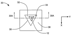
18 基板
102 基板支持組立体
104 チップ支持組立体
106 基部
108 固定具
110 基板ステージ組立体
112 x方向
114 y方向
116 z方向
118 アクチュエータ
120 第1ステージ
122 第2ステージ
124 第1アクチュエータ
126 第2アクチュエータ
130 チップステージ組立体
132 チップカンチレバー
134 アクチュエータ
136 コントローラ
138 手動ユーザ入力
140 メモリ
142 第1パッチ
144 第2パッチ
200 デブリ回収及び計測装置
202 計測システム
204 エネルギー源
206 エネルギー検出器
208 入射エネルギービーム
210 試料エネルギービーム
Claims (19)
- ナノスケール計測システムであって、
走査型プローブ顕微鏡(SPM)チップと、
入射する照射を前記SPMチップ上に配向するように構成され配置された照射源と、
前記入射する照射によって引き起こされた試料照射を前記SPMチップから受けるように構成され配置された照射検出器と、
前記ナノスケール計測システムに動作可能に連結され、前記SPMチップと前記照射源及び前記照射検出器のうちの少なくとも1つとの間の相対移動を生じるように構成されたアクチュエータシステムと、を有し、
前記アクチュエータシステムは、回収器と、前記照射源及び前記照射検出器の少なくとも一方との間で相対移動を生じるように構成されると共に、
前記アクチュエータシステムは、粒子又はデブリの少なくとも一方を、基板から前記SPMチップへ移送し、且つ前記SPMチップから前記回収器へ移送するように、前記回収器に対して前記SPMチップを移動させるように構成され、さらに、
前記アクチュエータシステム及び前記照射検出器に動作可能に連結されたコントローラを備え、前記コントローラが、
前記照射検出器から第1の信号を受け取るように、前記基板に近接した位置から計測位置へ前記SPMチップを移動させ、
前記試料照射に対する前記照射検出器の第1の応答に基づいて第1の信号を受け取り、
前記第1の信号に基づいて前記アクチュエータシステムを介して前記SPMチップと前記照射検出器及び前記照射源のうちの少なくとも1つとの間に相対移動を生じる、
ように構成されている、ナノスケール計測システム。 - 前記アクチュエータシステムは、前記SPMチップに動作可能に連結され、前記アクチュエータシステムは、第1の軸の周りで前記SPMチップを回転させるように構成された回転アクチュエータを含む、請求項1に記載のナノスケール計測システム。
- 前記照射源はレーザである、請求項1に記載のナノスケール計測システム。
- 前記コントローラは更に、
前記第1の信号に基づいて前記試料照射の第1の周波数領域スペクトルを生成し、
前記第1の周波数領域スペクトルからバックグラウンド周波数領域スペクトルを差し引くことによって第2の周波数領域スペクトルを生成し、
前記第2の周波数領域スペクトルに基づいて、前記アクチュエータシステムによって前記SPMチップと前記照射検出器及び前記照射源のうちの少なくとも1つとの間に相対移動を生じる、
ように構成されている、請求項1に記載のナノスケール計測システム。 - 前記コントローラは更に、前記SPMチップが実質的に汚染物質を含まない場合に、前記SPMチップの照射に対する前記照射検出器の応答に基づいて前記バックグラウンド周波数領域スペクトルを生成するよう構成されている、請求項4に記載のナノスケール計測システム。
- 前記コントローラは更に、
第2の試料照射に対する前記照射検出器の第2の応答に基づいて第2の信号を受信し、
前記第1の信号と前記第2の信号との間の差に基づいて前記アクチュエータシステムによって前記SPMチップと前記照射検出器及び前記照射源のうちの少なくとも1つとの間に相対移動を生じる、
ように構成される、請求項1に記載のナノスケール計測システム。 - 回収器を備えた計測システムであって、
前記回収器が、
前記回収器の第1の表面上に第1の内縁部と、
前記回収器の第2の表面上に前記第1の表面の反対側にある第2の内縁部と、
前記第1の内縁部から前記第2の内縁部まで延びて、回収ポケット又は回収スルーホールのうちの少なくとも一部を定める内部表面と、
を含み、
前記計測システムが更に、
入射する照射を前記回収器の内部表面上に配向するように構成され配置された照射源と、
前記入射する照射によって引き起こされる試料照射を前記回収器の内部表面から受けるように構成され配置された照射検出器と、
走査型プローブ顕微鏡(SPM)チップと、
前記SPMチップに動作可能に連結され、前記SPMチップを前記回収器に対して移動させて、少なくとも1つの粒子又はデブリを前記SPMチップから前記回収器に移送するように構成されるアクチュエータシステムと、
を備える計測システム。 - 前記回収スルーホールの幅は、前記第1の表面から前記第2の表面に向かって前記回収器を通過する方向に沿って増加する、請求項7に記載の計測システム。
- 記第1の内縁部は、前記回収ポケット又は前記回収スルーホールの矩形の輪郭を定める、請求項7に記載の計測システム。
- 前記第1の内縁部は、前記回収ポケット又は前記回収スルーホールの三角形の輪郭を定める、請求項7に記載の計測システム。
- 前記第1の内縁部は前記回収ポケット又は前記回収スルーホールの弓形断面を定め、前記弓形断面が、円形、楕円形又は卵形の輪郭である、請求項7に記載の計測システム。
- 粒子回収及び計測システムであって、
走査型プローブ顕微鏡(SPM)チップと、
基板を支持するように構成されたステージと、
前記ステージ及び前記SPMチップに動作可能に連結され、前記SPMチップを前記ステージに対して移動させるように構成された作動システムと、
計測位置と光学的に連通する照射源と、
前記計測位置と光学的に連通する照射検出器と、
前記計測位置が、その少なくとも一部に配置された粒子回収器と、
前記作動システム、前記照射源、及び前記照射検出器に動作可能に連結されたコントローラと、
を備え、
前記コントローラが、
前記基板に近接した位置から前記計測位置に前記SPMチップを移動させ、
前記計測位置からの第1の試料照射に対する前記照射検出器の応答を示す第1の信号を前記照射検出器から受信する、
ように構成され、
前記第1の試料照射が、前記照射源からの第1の入射する照射によって引き起こされ、
前記コントローラは、前記第1の入射する照射によって前記計測位置を照射することにより、前記第1の試料照射を行うように構成される、粒子回収及び計測システム。 - 前記計測位置は、前記SPMチップの少なくとも一部分上に配置され、前記コントローラは更に、前記第1の入射する照射を前記計測位置に照射することによって前記第1の試料照射を引き起こすように構成される、請求項12に記載の粒子回収及び計測システム。
- ナノスケール計測システムであって、
走査型プローブ顕微鏡(SPM)チップと、
基板を指示するように構成されたステージと、
パッチと、
入射する照射を前記SPMチップ上に配向するように構成され配置された照射源と、
前記入射する照射によって引き起こされた試料照射を前記SPMチップから受けるように構成され配置された照射検出器と、
前記ナノスケール計測システムに動作可能に連結され、前記SPMチップと、粒子又はデブリの少なくとも一方を前記基板から前記SPMチップへ移送するための前記ステージとの間の相対移動を生じさせるように構成されたアクチュエータシステムと、を有し、
前記アクチュエータシステムは、粒子又はデブリの少なくとも一方の、前記SPMチップから前記パッチへの移送を行うために、前記パッチに対して前記SPMチップを移動させるように構成され、さらに、
前記アクチュエータシステム及び前記照射検出器に動作可能に連結されたコントローラを備え、前記コントローラが、
前記照射検出器から第1の信号を受け取るように、前記基板に近接した位置から計測位置へ前記SPMチップを移動させ、
前記試料照射に対する前記照射検出器の第1の応答に基づいて第1の信号を受け取り、
前記SPMチップ上の粒子又はデブリの少なくとも一方の、材料属性を特定するように前記第1の信号を解析する、ナノスケール計測システム。 - 前記アクチュエータシステムは、前記SPMチップと、前記照射検出器及び前記照射源の少なくとも一方との間の相対移動を生じさせるように構成され、前記コントローラは、前記第1の信号に基づいて、前記アクチュエータシステムに、前記SPMチップと、前記照射検出器及び前記照射源の少なくとも一方との間の相対移動を生じさせる請求項14記載の計測システム。
- 前記照射源はレーザである、請求項14又は15に記載の計測システム。
- 前記コントローラは更に、
前記第1の信号に基づいて前記試料照射の第1の周波数領域スペクトルを生成し、
前記第1の周波数領域スペクトルからバックグラウンド周波数領域スペクトルを差し引くことによって第2の周波数領域スペクトルを生成し、
前記第2の周波数領域スペクトルに基づいて、前記アクチュエータシステムによって前記SPMチップと前記照射検出器及び前記照射源のうちの少なくとも1つとの間に相対移動を生じる、
ように構成されている、請求項15に記載の計測システム。 - 前記パッチは、前記粒子又はデブリの少なくとも一方を、その中に機械的に詰め込むために十分に柔軟なパッチ材料を有する請求項14乃至17の何れか1項に記載の計測システム。
- 前記照射源は電子ビーム源であり、前記照射検出器はX線検出器である、請求項1、2、4乃至13、及び14乃至17の何れか1項に記載の計測システム。
Applications Claiming Priority (2)
| Application Number | Priority Date | Filing Date | Title |
|---|---|---|---|
| US15/160,263 | 2016-05-20 | ||
| US15/160,263 US10384238B2 (en) | 2007-09-17 | 2016-05-20 | Debris removal in high aspect structures |
Publications (3)
| Publication Number | Publication Date |
|---|---|
| JP2017207755A JP2017207755A (ja) | 2017-11-24 |
| JP2017207755A5 JP2017207755A5 (ja) | 2020-08-13 |
| JP7042039B2 true JP7042039B2 (ja) | 2022-03-25 |
Family
ID=58772394
Family Applications (1)
| Application Number | Title | Priority Date | Filing Date |
|---|---|---|---|
| JP2017100801A Active JP7042039B2 (ja) | 2016-05-20 | 2017-05-22 | 高アスペクト構造からのデブリ除去 |
Country Status (4)
| Country | Link |
|---|---|
| EP (1) | EP3251760A1 (ja) |
| JP (1) | JP7042039B2 (ja) |
| KR (1) | KR102433627B1 (ja) |
| TW (1) | TWI787181B (ja) |
Families Citing this family (2)
| Publication number | Priority date | Publication date | Assignee | Title |
|---|---|---|---|---|
| EP3964841A1 (de) | 2020-09-02 | 2022-03-09 | Siltronic AG | Messapparatur und verfahren zum untersuchen eines bereichs einer oberfläche eines substrats mit hilfe einer kraft-messsonde |
| DE102021201669B4 (de) * | 2021-02-22 | 2023-08-17 | Carl Zeiss Smt Gmbh | Verfahren und vorrichtung zum bearbeiten einer probe |
Citations (8)
| Publication number | Priority date | Publication date | Assignee | Title |
|---|---|---|---|---|
| JP2008512573A (ja) | 2004-09-03 | 2008-04-24 | ハネウェル・インターナショナル・インコーポレーテッド | 延伸ゲルスパンポリエチレンヤーン及び延伸のための方法 |
| JP2008145242A (ja) | 2006-12-08 | 2008-06-26 | Sii Nanotechnology Inc | 原子間力顕微鏡の加工用ダイヤモンド探針の観察方法及び加工方法 |
| JP2008209544A (ja) | 2007-02-26 | 2008-09-11 | Sii Nanotechnology Inc | フォトマスク上の異物の組成分析方法 |
| JP2009006378A (ja) | 2007-06-29 | 2009-01-15 | Sii Nanotechnology Inc | 微細加工方法及び微細加工装置 |
| JP2009103571A (ja) | 2007-10-23 | 2009-05-14 | Canon Inc | 近接場光散乱用プローブおよびその製造方法 |
| JP2010539714A (ja) | 2007-09-17 | 2010-12-16 | レイヴ,エルエルシー | 高アスペクト構造における破片除去 |
| CN102798735A (zh) | 2012-08-14 | 2012-11-28 | 厦门大学 | 针尖增强暗场显微镜、电化学测试装置和调平系统 |
| JP2015108570A (ja) | 2013-12-05 | 2015-06-11 | 株式会社日立ハイテクマニファクチャ&サービス | 顕微ラマン分光装置および顕微ラマン分光システム |
Family Cites Families (6)
| Publication number | Priority date | Publication date | Assignee | Title |
|---|---|---|---|---|
| JPH05164512A (ja) * | 1991-12-13 | 1993-06-29 | Toshiba Corp | 表面測定装置 |
| TW285721B (ja) * | 1994-12-27 | 1996-09-11 | Siemens Ag | |
| JP2005084582A (ja) * | 2003-09-11 | 2005-03-31 | Sii Nanotechnology Inc | フォトマスクのパーティクル除去方法 |
| JP2006339472A (ja) * | 2005-06-03 | 2006-12-14 | Matsushita Electric Ind Co Ltd | プローブカード触針のクリーニング装置およびクリーニング方法 |
| JP2009265176A (ja) * | 2008-04-22 | 2009-11-12 | Toshiba Corp | 異物除去方法、異物除去装置および半導体装置の作製方法 |
| JP2011133296A (ja) * | 2009-12-24 | 2011-07-07 | Yamaha Corp | クリーニング装置、及び、プローブ針のクリーニング方法 |
-
2017
- 2017-05-02 TW TW106114454A patent/TWI787181B/zh active
- 2017-05-18 KR KR1020170061709A patent/KR102433627B1/ko active IP Right Grant
- 2017-05-22 EP EP17172132.7A patent/EP3251760A1/en active Pending
- 2017-05-22 JP JP2017100801A patent/JP7042039B2/ja active Active
Patent Citations (8)
| Publication number | Priority date | Publication date | Assignee | Title |
|---|---|---|---|---|
| JP2008512573A (ja) | 2004-09-03 | 2008-04-24 | ハネウェル・インターナショナル・インコーポレーテッド | 延伸ゲルスパンポリエチレンヤーン及び延伸のための方法 |
| JP2008145242A (ja) | 2006-12-08 | 2008-06-26 | Sii Nanotechnology Inc | 原子間力顕微鏡の加工用ダイヤモンド探針の観察方法及び加工方法 |
| JP2008209544A (ja) | 2007-02-26 | 2008-09-11 | Sii Nanotechnology Inc | フォトマスク上の異物の組成分析方法 |
| JP2009006378A (ja) | 2007-06-29 | 2009-01-15 | Sii Nanotechnology Inc | 微細加工方法及び微細加工装置 |
| JP2010539714A (ja) | 2007-09-17 | 2010-12-16 | レイヴ,エルエルシー | 高アスペクト構造における破片除去 |
| JP2009103571A (ja) | 2007-10-23 | 2009-05-14 | Canon Inc | 近接場光散乱用プローブおよびその製造方法 |
| CN102798735A (zh) | 2012-08-14 | 2012-11-28 | 厦门大学 | 针尖增强暗场显微镜、电化学测试装置和调平系统 |
| JP2015108570A (ja) | 2013-12-05 | 2015-06-11 | 株式会社日立ハイテクマニファクチャ&サービス | 顕微ラマン分光装置および顕微ラマン分光システム |
Also Published As
| Publication number | Publication date |
|---|---|
| EP3251760A1 (en) | 2017-12-06 |
| KR20170131264A (ko) | 2017-11-29 |
| TW202313219A (zh) | 2023-04-01 |
| JP2017207755A (ja) | 2017-11-24 |
| TWI787181B (zh) | 2022-12-21 |
| KR102433627B1 (ko) | 2022-08-18 |
| TW201805078A (zh) | 2018-02-16 |
Similar Documents
| Publication | Publication Date | Title |
|---|---|---|
| US11040379B2 (en) | Debris removal in high aspect structures | |
| US11391664B2 (en) | Debris removal from high aspect structures | |
| JP2022050485A (ja) | 高アスペクト構造からのデブリ除去 | |
| EP3726566B1 (en) | Debris removal from a trench formed on a photolithographic mask | |
| US10618080B2 (en) | Debris removal from high aspect structures | |
| JP7042039B2 (ja) | 高アスペクト構造からのデブリ除去 | |
| TWI841110B (zh) | 從高深寬比結構移除碎片 | |
| EP3748431B1 (en) | Debris removal from high aspect structures | |
| JP7495087B2 (ja) | 高アスペクト構造からのデブリ除去 |
Legal Events
| Date | Code | Title | Description |
|---|---|---|---|
| A521 | Request for written amendment filed |
Free format text: JAPANESE INTERMEDIATE CODE: A523 Effective date: 20200522 |
|
| A621 | Written request for application examination |
Free format text: JAPANESE INTERMEDIATE CODE: A621 Effective date: 20200522 |
|
| A521 | Request for written amendment filed |
Free format text: JAPANESE INTERMEDIATE CODE: A523 Effective date: 20200629 |
|
| A977 | Report on retrieval |
Free format text: JAPANESE INTERMEDIATE CODE: A971007 Effective date: 20210408 |
|
| A131 | Notification of reasons for refusal |
Free format text: JAPANESE INTERMEDIATE CODE: A131 Effective date: 20210510 |
|
| A601 | Written request for extension of time |
Free format text: JAPANESE INTERMEDIATE CODE: A601 Effective date: 20210810 |
|
| A521 | Request for written amendment filed |
Free format text: JAPANESE INTERMEDIATE CODE: A523 Effective date: 20211006 |
|
| TRDD | Decision of grant or rejection written | ||
| A01 | Written decision to grant a patent or to grant a registration (utility model) |
Free format text: JAPANESE INTERMEDIATE CODE: A01 Effective date: 20220113 |
|
| A601 | Written request for extension of time |
Free format text: JAPANESE INTERMEDIATE CODE: A601 Effective date: 20220214 |
|
| A61 | First payment of annual fees (during grant procedure) |
Free format text: JAPANESE INTERMEDIATE CODE: A61 Effective date: 20220314 |
|
| R150 | Certificate of patent or registration of utility model |
Ref document number: 7042039 Country of ref document: JP Free format text: JAPANESE INTERMEDIATE CODE: R150 |