JP6991981B2 - 光エミッタのための薄型相互接続子 - Google Patents
光エミッタのための薄型相互接続子 Download PDFInfo
- Publication number
- JP6991981B2 JP6991981B2 JP2018542727A JP2018542727A JP6991981B2 JP 6991981 B2 JP6991981 B2 JP 6991981B2 JP 2018542727 A JP2018542727 A JP 2018542727A JP 2018542727 A JP2018542727 A JP 2018542727A JP 6991981 B2 JP6991981 B2 JP 6991981B2
- Authority
- JP
- Japan
- Prior art keywords
- light
- optical
- light emitter
- electrical
- display system
- Prior art date
- Legal status (The legal status is an assumption and is not a legal conclusion. Google has not performed a legal analysis and makes no representation as to the accuracy of the status listed.)
- Active
Links
Images


Classifications
-
- H—ELECTRICITY
- H10—SEMICONDUCTOR DEVICES; ELECTRIC SOLID-STATE DEVICES NOT OTHERWISE PROVIDED FOR
- H10H—INORGANIC LIGHT-EMITTING SEMICONDUCTOR DEVICES HAVING POTENTIAL BARRIERS
- H10H20/00—Individual inorganic light-emitting semiconductor devices having potential barriers, e.g. light-emitting diodes [LED]
- H10H20/80—Constructional details
- H10H20/85—Packages
- H10H20/857—Interconnections, e.g. lead-frames, bond wires or solder balls
-
- G—PHYSICS
- G02—OPTICS
- G02B—OPTICAL ELEMENTS, SYSTEMS OR APPARATUS
- G02B27/00—Optical systems or apparatus not provided for by any of the groups G02B1/00 - G02B26/00, G02B30/00
- G02B27/01—Head-up displays
- G02B27/017—Head mounted
-
- G—PHYSICS
- G09—EDUCATION; CRYPTOGRAPHY; DISPLAY; ADVERTISING; SEALS
- G09F—DISPLAYING; ADVERTISING; SIGNS; LABELS OR NAME-PLATES; SEALS
- G09F9/00—Indicating arrangements for variable information in which the information is built-up on a support by selection or combination of individual elements
- G09F9/30—Indicating arrangements for variable information in which the information is built-up on a support by selection or combination of individual elements in which the desired character or characters are formed by combining individual elements
- G09F9/33—Indicating arrangements for variable information in which the information is built-up on a support by selection or combination of individual elements in which the desired character or characters are formed by combining individual elements being semiconductor devices, e.g. diodes
-
- G—PHYSICS
- G02—OPTICS
- G02B—OPTICAL ELEMENTS, SYSTEMS OR APPARATUS
- G02B27/00—Optical systems or apparatus not provided for by any of the groups G02B1/00 - G02B26/00, G02B30/00
- G02B27/01—Head-up displays
- G02B27/017—Head mounted
- G02B27/0172—Head mounted characterised by optical features
-
- G—PHYSICS
- G02—OPTICS
- G02B—OPTICAL ELEMENTS, SYSTEMS OR APPARATUS
- G02B6/00—Light guides; Structural details of arrangements comprising light guides and other optical elements, e.g. couplings
- G02B6/0001—Light guides; Structural details of arrangements comprising light guides and other optical elements, e.g. couplings specially adapted for lighting devices or systems
- G02B6/0005—Light guides; Structural details of arrangements comprising light guides and other optical elements, e.g. couplings specially adapted for lighting devices or systems the light guides being of the fibre type
- G02B6/001—Light guides; Structural details of arrangements comprising light guides and other optical elements, e.g. couplings specially adapted for lighting devices or systems the light guides being of the fibre type the light being emitted along at least a portion of the lateral surface of the fibre
-
- G—PHYSICS
- G02—OPTICS
- G02B—OPTICAL ELEMENTS, SYSTEMS OR APPARATUS
- G02B6/00—Light guides; Structural details of arrangements comprising light guides and other optical elements, e.g. couplings
- G02B6/0001—Light guides; Structural details of arrangements comprising light guides and other optical elements, e.g. couplings specially adapted for lighting devices or systems
- G02B6/0011—Light guides; Structural details of arrangements comprising light guides and other optical elements, e.g. couplings specially adapted for lighting devices or systems the light guides being planar or of plate-like form
- G02B6/0013—Means for improving the coupling-in of light from the light source into the light guide
- G02B6/0023—Means for improving the coupling-in of light from the light source into the light guide provided by one optical element, or plurality thereof, placed between the light guide and the light source, or around the light source
- G02B6/0028—Light guide, e.g. taper
-
- G—PHYSICS
- G02—OPTICS
- G02B—OPTICAL ELEMENTS, SYSTEMS OR APPARATUS
- G02B6/00—Light guides; Structural details of arrangements comprising light guides and other optical elements, e.g. couplings
- G02B6/0001—Light guides; Structural details of arrangements comprising light guides and other optical elements, e.g. couplings specially adapted for lighting devices or systems
- G02B6/0011—Light guides; Structural details of arrangements comprising light guides and other optical elements, e.g. couplings specially adapted for lighting devices or systems the light guides being planar or of plate-like form
- G02B6/0033—Means for improving the coupling-out of light from the light guide
- G02B6/005—Means for improving the coupling-out of light from the light guide provided by one optical element, or plurality thereof, placed on the light output side of the light guide
-
- G—PHYSICS
- G02—OPTICS
- G02B—OPTICAL ELEMENTS, SYSTEMS OR APPARATUS
- G02B6/00—Light guides; Structural details of arrangements comprising light guides and other optical elements, e.g. couplings
- G02B6/0001—Light guides; Structural details of arrangements comprising light guides and other optical elements, e.g. couplings specially adapted for lighting devices or systems
- G02B6/0011—Light guides; Structural details of arrangements comprising light guides and other optical elements, e.g. couplings specially adapted for lighting devices or systems the light guides being planar or of plate-like form
- G02B6/0075—Arrangements of multiple light guides
- G02B6/0076—Stacked arrangements of multiple light guides of the same or different cross-sectional area
-
- H—ELECTRICITY
- H05—ELECTRIC TECHNIQUES NOT OTHERWISE PROVIDED FOR
- H05K—PRINTED CIRCUITS; CASINGS OR CONSTRUCTIONAL DETAILS OF ELECTRIC APPARATUS; MANUFACTURE OF ASSEMBLAGES OF ELECTRICAL COMPONENTS
- H05K1/00—Printed circuits
- H05K1/18—Printed circuits structurally associated with non-printed electric components
- H05K1/182—Printed circuits structurally associated with non-printed electric components associated with components mounted in printed circuit boards [PCB], e.g. insert-mounted components [IMC]
-
- H—ELECTRICITY
- H10—SEMICONDUCTOR DEVICES; ELECTRIC SOLID-STATE DEVICES NOT OTHERWISE PROVIDED FOR
- H10H—INORGANIC LIGHT-EMITTING SEMICONDUCTOR DEVICES HAVING POTENTIAL BARRIERS
- H10H20/00—Individual inorganic light-emitting semiconductor devices having potential barriers, e.g. light-emitting diodes [LED]
- H10H20/80—Constructional details
- H10H20/83—Electrodes
-
- G—PHYSICS
- G02—OPTICS
- G02B—OPTICAL ELEMENTS, SYSTEMS OR APPARATUS
- G02B27/00—Optical systems or apparatus not provided for by any of the groups G02B1/00 - G02B26/00, G02B30/00
- G02B27/01—Head-up displays
- G02B27/0101—Head-up displays characterised by optical features
- G02B2027/0118—Head-up displays characterised by optical features comprising devices for improving the contrast of the display / brillance control visibility
-
- G—PHYSICS
- G02—OPTICS
- G02B—OPTICAL ELEMENTS, SYSTEMS OR APPARATUS
- G02B27/00—Optical systems or apparatus not provided for by any of the groups G02B1/00 - G02B26/00, G02B30/00
- G02B27/01—Head-up displays
- G02B27/0101—Head-up displays characterised by optical features
- G02B2027/0132—Head-up displays characterised by optical features comprising binocular systems
- G02B2027/0134—Head-up displays characterised by optical features comprising binocular systems of stereoscopic type
-
- G—PHYSICS
- G02—OPTICS
- G02B—OPTICAL ELEMENTS, SYSTEMS OR APPARATUS
- G02B27/00—Optical systems or apparatus not provided for by any of the groups G02B1/00 - G02B26/00, G02B30/00
- G02B27/01—Head-up displays
- G02B27/017—Head mounted
- G02B2027/0178—Eyeglass type
-
- H—ELECTRICITY
- H10—SEMICONDUCTOR DEVICES; ELECTRIC SOLID-STATE DEVICES NOT OTHERWISE PROVIDED FOR
- H10H—INORGANIC LIGHT-EMITTING SEMICONDUCTOR DEVICES HAVING POTENTIAL BARRIERS
- H10H20/00—Individual inorganic light-emitting semiconductor devices having potential barriers, e.g. light-emitting diodes [LED]
- H10H20/01—Manufacture or treatment
- H10H20/036—Manufacture or treatment of packages
- H10H20/0364—Manufacture or treatment of packages of interconnections
-
- H—ELECTRICITY
- H10—SEMICONDUCTOR DEVICES; ELECTRIC SOLID-STATE DEVICES NOT OTHERWISE PROVIDED FOR
- H10H—INORGANIC LIGHT-EMITTING SEMICONDUCTOR DEVICES HAVING POTENTIAL BARRIERS
- H10H20/00—Individual inorganic light-emitting semiconductor devices having potential barriers, e.g. light-emitting diodes [LED]
- H10H20/80—Constructional details
- H10H20/83—Electrodes
- H10H20/831—Electrodes characterised by their shape
- H10H20/8314—Electrodes characterised by their shape extending at least partially onto an outer side surface of the bodies
-
- H—ELECTRICITY
- H10—SEMICONDUCTOR DEVICES; ELECTRIC SOLID-STATE DEVICES NOT OTHERWISE PROVIDED FOR
- H10H—INORGANIC LIGHT-EMITTING SEMICONDUCTOR DEVICES HAVING POTENTIAL BARRIERS
- H10H20/00—Individual inorganic light-emitting semiconductor devices having potential barriers, e.g. light-emitting diodes [LED]
- H10H20/80—Constructional details
- H10H20/85—Packages
- H10H20/852—Encapsulations
-
- H—ELECTRICITY
- H10—SEMICONDUCTOR DEVICES; ELECTRIC SOLID-STATE DEVICES NOT OTHERWISE PROVIDED FOR
- H10W—GENERIC PACKAGES, INTERCONNECTIONS, CONNECTORS OR OTHER CONSTRUCTIONAL DETAILS OF DEVICES COVERED BY CLASS H10
- H10W72/00—Interconnections or connectors in packages
- H10W72/851—Dispositions of multiple connectors or interconnections
- H10W72/874—On different surfaces
- H10W72/884—Die-attach connectors and bond wires
-
- H—ELECTRICITY
- H10—SEMICONDUCTOR DEVICES; ELECTRIC SOLID-STATE DEVICES NOT OTHERWISE PROVIDED FOR
- H10W—GENERIC PACKAGES, INTERCONNECTIONS, CONNECTORS OR OTHER CONSTRUCTIONAL DETAILS OF DEVICES COVERED BY CLASS H10
- H10W90/00—Package configurations
Landscapes
- Physics & Mathematics (AREA)
- General Physics & Mathematics (AREA)
- Optics & Photonics (AREA)
- Engineering & Computer Science (AREA)
- Microelectronics & Electronic Packaging (AREA)
- Theoretical Computer Science (AREA)
- Non-Portable Lighting Devices Or Systems Thereof (AREA)
- Devices For Indicating Variable Information By Combining Individual Elements (AREA)
- Led Device Packages (AREA)
- Led Devices (AREA)
- Testing, Inspecting, Measuring Of Stereoscopic Televisions And Televisions (AREA)
- Planar Illumination Modules (AREA)
- Fastening Of Light Sources Or Lamp Holders (AREA)
- Cathode-Ray Tubes And Fluorescent Screens For Display (AREA)
- Optical Integrated Circuits (AREA)
- Optical Couplings Of Light Guides (AREA)
Description
本出願は、35U.S.C.§119(e)の下で2016年2月24日に出願された「LOW PROFILE INTERCONNECT FOR LIGHT EMITTER」という題目の米国仮出願第62/299,163号の優先利益を主張する。上記文献の開示内容は、その全体として参照することによって本明細書において援用される。
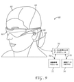
本開示は、光源に関し、より具体的には、基板上に搭載される光エミッタを伴う、光源に関する。いくつかの実施形態では、光エミッタは、発光ダイオードであってもよい。
(関連技術の説明)
基板上に搭載される光エミッタ(回路基板上に搭載される発光ダイオード等)は、光源として使用され、照明を種々の電子デバイス内に提供する。基板は、電力を光エミッタに提供するために、光エミッタを基板上の配線と接続する配線接合を含んでもよい。現代のデバイスに関する仕様が変化するにつれて、例えば、効率、ロバスト性、および/またはコンパクト性に関する要件が増加するにつれて、これらの現代のデバイスの必要性を満たすことができる、光源を開発する継続的必要がある。
いくつかの実施形態では、照明システムが、提供される。照明システムは、基板接合パッドを備える、基板を備える。光エミッタが、基板に取り付けられ、光エミッタは、光エミッタ接合パッドを備える。電気相互接続子が、光エミッタにわたってある。電気相互接続子は、電気相互接続子の一端において、光エミッタ接合パッドに接触し、電気相互接続子の他端において、基板接合パッドに接触する。電気相互接続子の断面形状は、電気相互接続子の伸長軸に対して横切る平面において見ると、高さより大きい幅を有する。光エミッタの上方の電気相互接続子の最大高さは、いくつかの実施形態では、50μm以下であってもよい。電気相互接続子は、いくつかの実施形態では、光エミッタの輪郭に共形状に追従してもよい。
本明細書は、例えば、以下の項目も提供する。
(項目1)
照明システムであって、
基板接合パッドを備える基板と、
前記基板に取り付けられた光エミッタであって、前記光エミッタは、光エミッタ接合パッドを備える、光エミッタと、
前記光エミッタにわたる電気相互接続子であって、前記電気相互接続子は、前記電気相互接続子の一端において前記光エミッタ接合パッドに接触し、前記電気相互接続子の他端において前記基板接合パッドに接触する、電気相互接続子と
を備え、
前記電気相互接続子の断面形状は、前記電気相互接続子の伸長軸に対して横切る平面において見ると、前記断面形状の高さより大きい幅を有する、照明システム。
(項目2)
前記光エミッタの上方の前記電気相互接続子の最大高さは、50μm以下である、項目1に記載の照明システム。
(項目3)
前記電気相互接続子は、前記光エミッタの輪郭に共形状に追従する、項目1に記載の照明システム。
(項目4)
前記光エミッタは、前記基板にわたって段を画定し、前記電気相互接続子は、前記段の輪郭に追従する、項目3に記載の照明システム。
(項目5)
前記断面形状は、長方形である、項目1に記載の照明システム。
(項目6)
前記電気相互接続子は、金属を備える、項目1に記載の照明システム。
(項目7)
前記光エミッタは、LEDチップである、項目1に記載の照明システム。
(項目8)
前記基板は、印刷回路基板である、項目1に記載の照明システム。
(項目9)
前記光エミッタと前記電気相互接続子との間に誘電層をさらに備える、項目1に記載の照明システム。
(項目10)
前記光エミッタはさらに、他の光エミッタ接合パッドと、他の電気相互接続子とを備え、
前記他の電気相互接続子は、前記他の電気相互接続子の一端において前記他の光エミッタ接合パッドに接触し、前記電気相互接続子の他端において他の基板接合パッドに接触し、
前記他の電気相互接続子の断面形状は、前記電気相互接続子の伸長軸に対して横切る平面において見ると、高さより大きい幅を有する、項目1に記載の照明システム。
(項目11)
前記光エミッタの暴露表面にわたる光パイプをさらに備える、項目1に記載の照明システム。
(項目12)
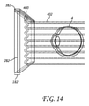
前記光パイプから光を受信するように構成された光変調デバイスと、
導波管のスタックであって、各導波管は、前記光変調デバイスから光を受信するように構成された光内部結合光学要素を備える、導波管のスタックと
をさらに備える、項目11に記載の照明システム。
(項目13)
複数の前記光パイプをさらに備え、各光パイプは、光を前記光変調デバイスに伝送するように構成されている、項目12に記載の照明システム。
(項目14)
前記光エミッタの暴露表面にわたる反射体をさらに備える、項目1に記載の照明システム。
(項目15)
前記反射体から光を受信するように構成された光変調デバイスと、
導波管のスタックであって、各導波管は、前記光変調デバイスから光を受信するように構成された光内部結合光学要素を備える、導波管のスタックと
をさらに備える、項目14に記載の照明システム。
(項目16)
複数の前記反射体をさらに備え、各反射体は、光を前記光変調デバイスに指向するように構成されている、項目14に記載の照明システム。
(項目17)
照明デバイスを作製するための方法であって、
基板接合パッドを備える基板にわたって、光エミッタを提供することであって、前記光エミッタは、光エミッタ接合パッドを備える、ことと、
前記光エミッタにわたって、かつ前記光エミッタ接合パッドおよび前記基板接合パッドと接触するように、電気相互接続子を堆積させることと
を含む、方法。
(項目18)
前記電気相互接続子を堆積させることは、前記電気相互接続子を3D印刷することを含む、項目17に記載の方法。
(項目19)
前記電気相互接続子を堆積させる前に、誘電材料を前記光エミッタにわたって堆積させることをさらに含む、項目17に記載の方法。
(項目20)
前記誘電材料を堆積させることは、前記誘電材料を3D印刷することを含む、項目17に記載の方法。
(項目21)
前記電気相互接続子を堆積させることは、金属を堆積させることを含む、項目17に記載の方法。
(項目22)
前記光エミッタは、LEDチップである、項目17に記載の方法。
(項目23)
前記光エミッタの上方の前記電気相互接続子の最大高さは、50μm以下である、項目17に記載の方法。
(項目24)
光パイプを前記光エミッタに結合することをさらに含み、前記光パイプの光入力表面は、前記光エミッタの暴露表面に面する、項目17に記載の方法。
(項目25)
反射体を前記光エミッタに結合することをさらに含み、前記反射体の光入力表面は、前記光エミッタの暴露表面に面する、項目17に記載の方法。
(項目26)
前記光エミッタを提供することは、前記光エミッタを前記基板の表面上の電気接点上に取り付けることを含む、項目17に記載の方法。
光エミッタは、光エミッタから光を受信し、例えば、さらに、その光を伝送し、および/または光を修正する、上層光学構造(例えば、光パイプ)に結合されてもよい。光エミッタから光学構造の中への光の投入の効率は、光エミッタと光学構造を分離する距離に大きく依存することを理解されたい。分離が小さいほど、より高い効率を提供し、光学構造の中に投入される放出される光の割合も高くなる。より小さい分離の影響は、光学構造および光エミッタの幅または横寸法における減少に伴って増加し得る。すなわち、横寸法が減少するにつれて、より多くの電力が、光学構造から逸失する光によって縁の周囲で喪失される。例えば、横方向における光学構造および光エミッタ寸法が、1.5mmより小さい場合、効率に及ぼす分離の影響は、容易に明白となる。したがって、光エミッタと光エミッタから光を受信する光学構造との間の分離の影響は、光エミッタおよび光学構造の表面の断面積が減少するにつれて増加する。
ここで、同様の参照番号が全体を通して同様の部品を指す、図面を参照する。
薄型相互接続子は、光エミッタにわたる薄型が所望される、種々の照明用途において利用されてもよいことを理解されたい。本明細書に議論されるように、薄型は、光エミッタと光パイプ等の上層光学構造との間の緊密間隔を提供することができる。本緊密間隔は、光エミッタから光パイプの中への光の非常に効率的伝達を可能にすることができる。別の利点は、配線接合を排除することによって、相互接続子が、衝撃および振動ならびに環境懸念に対してよりロバストとなることができることである。加えて、これらの相互接続子は、光源がともにより近接して設置されることを可能にし得、これは、所与のレベルの出力のために、光学システムをより小型かつより軽量にすることができる。そのような高効率、ロバスト性、および小サイズは、有利には、ディスプレイデバイス内に利用され、明るさおよび可搬性を増加させ、および/またはディスプレイの電力使用を低減させ得る。
Claims (13)
- ディスプレイシステムであって、
複数の基板接合パッドを備える基板と、
前記基板に取り付けられた光エミッタのアレイであって、前記光エミッタの各々は、光エミッタ接合パッドを備える、光エミッタのアレイと、
複数の電気相互接続子であって、前記電気相互接続子の各々は、前記複数の光エミッタのうちの関連付けられた光エミッタにわたって位置付けられ、前記電気相互接続子は、前記電気相互接続子の一端において前記関連付けられた光エミッタの前記光エミッタ接合パッドに接触し、前記電気相互接続子の他端において前記関連付けられた光エミッタの前記基板接合パッドに接触する、複数の電気相互接続子と、
入射光を修正することにより画像を形成するように構成された空間光変調器と、
複数の光コレクタであって、前記光コレクタの各々は、前記光エミッタのアレイのうちの対応する光エミッタの暴露表面にわたって位置付けられ、前記光コレクタは、光を受けて前記空間光変調器に指向するように構成される、複数の光コレクタと
を備え、
前記光コレクタの各々は、対応する光エミッタの電気相互接続子の暴露表面から空隙によって離間され、
前記電気相互接続子は、前記光エミッタの輪郭に共形状に追従し、
前記電気相互接続子の各々の断面形状は、前記電気相互接続子の伸長軸に対して横切る平面において見ると、50倍以上前記断面形状の高さより大きい幅を有する、ディスプレイシステム。 - 前記光エミッタの各々の上方の前記電気相互接続子の最大高さは、50μm以下である、請求項1に記載のディスプレイシステム。
- 前記光エミッタの各々は、前記基板にわたって段を画定し、前記電気相互接続子は、前記関連付けられた光エミッタの各々の前記段の輪郭に追従する、請求項1に記載のディスプレイシステム。
- 前記断面形状は、長方形である、請求項1に記載のディスプレイシステム。
- 前記電気相互接続子の各々は、金属を備える、請求項1に記載のディスプレイシステム。
- 前記光エミッタの各々は、LEDチップである、請求項1に記載のディスプレイシステム。
- 前記基板は、印刷回路基板である、請求項1に記載のディスプレイシステム。
- 前記光エミッタの各々と前記関連付けられた電気相互接続子との間に誘電層をさらに備える、請求項1に記載のディスプレイシステム。
- 前記光エミッタの各々はさらに、他の光エミッタ接合パッドを備え、
複数の他の電気相互接続子をさらに備え、前記他の電気相互接続子の各々は、前記他の電気相互接続子の一端において前記光エミッタの各々の前記他の光エミッタ接合パッドに接触し、前記他の電気相互接続子の他端において他の基板接合パッドに接触し、
前記他の電気相互接続子の断面形状は、前記他の電気相互接続子の伸長軸に対して横切る平面において見ると、高さより大きい幅を有する、請求項1に記載のディスプレイシステム。 - 前記光コレクタは、光パイプである、請求項1に記載のディスプレイシステム。
- 導波管のスタックをさらに備え、各導波管は、前記空間光変調器から光を受けるように構成された光内部結合光学要素を備える、請求項10に記載のディスプレイシステム。
- 反射体のアレイをさらに備え、各反射体は、関連付けられた光エミッタの暴露表面にわたる、請求項1に記載のディスプレイシステム。
- 導波管のスタックをさらに備え、各導波管は、前記空間光変調器から光を受けるように構成された光内部結合光学要素を備える、請求項12に記載のディスプレイシステム。
Priority Applications (1)
| Application Number | Priority Date | Filing Date | Title |
|---|---|---|---|
| JP2021199078A JP7301116B2 (ja) | 2016-02-24 | 2021-12-08 | 光エミッタのための薄型相互接続子 |
Applications Claiming Priority (3)
| Application Number | Priority Date | Filing Date | Title |
|---|---|---|---|
| US201662299163P | 2016-02-24 | 2016-02-24 | |
| US62/299,163 | 2016-02-24 | ||
| PCT/US2017/019178 WO2017147322A1 (en) | 2016-02-24 | 2017-02-23 | Low profile interconnect for light emitter |
Related Child Applications (1)
| Application Number | Title | Priority Date | Filing Date |
|---|---|---|---|
| JP2021199078A Division JP7301116B2 (ja) | 2016-02-24 | 2021-12-08 | 光エミッタのための薄型相互接続子 |
Publications (2)
| Publication Number | Publication Date |
|---|---|
| JP2019509631A JP2019509631A (ja) | 2019-04-04 |
| JP6991981B2 true JP6991981B2 (ja) | 2022-01-13 |
Family
ID=59629515
Family Applications (2)
| Application Number | Title | Priority Date | Filing Date |
|---|---|---|---|
| JP2018542727A Active JP6991981B2 (ja) | 2016-02-24 | 2017-02-23 | 光エミッタのための薄型相互接続子 |
| JP2021199078A Active JP7301116B2 (ja) | 2016-02-24 | 2021-12-08 | 光エミッタのための薄型相互接続子 |
Family Applications After (1)
| Application Number | Title | Priority Date | Filing Date |
|---|---|---|---|
| JP2021199078A Active JP7301116B2 (ja) | 2016-02-24 | 2021-12-08 | 光エミッタのための薄型相互接続子 |
Country Status (10)
| Country | Link |
|---|---|
| US (4) | US11264548B2 (ja) |
| EP (2) | EP3420270B1 (ja) |
| JP (2) | JP6991981B2 (ja) |
| KR (2) | KR20250007679A (ja) |
| CN (2) | CN114898675A (ja) |
| AU (2) | AU2017223716B2 (ja) |
| IL (2) | IL261102B2 (ja) |
| NZ (1) | NZ745229A (ja) |
| TW (1) | TWI720140B (ja) |
| WO (1) | WO2017147322A1 (ja) |
Families Citing this family (6)
| Publication number | Priority date | Publication date | Assignee | Title |
|---|---|---|---|---|
| JP6991981B2 (ja) | 2016-02-24 | 2022-01-13 | マジック リープ, インコーポレイテッド | 光エミッタのための薄型相互接続子 |
| US20200081444A1 (en) * | 2018-01-12 | 2020-03-12 | Hong Huang | Cleaning method capable of automatically planning path |
| US10914945B2 (en) | 2018-11-09 | 2021-02-09 | Facebook Technologies, Llc | Inconspicuous near-eye electrical circuits |
| US20200150425A1 (en) * | 2018-11-09 | 2020-05-14 | Facebook Technologies, Llc | Inconspicuous near-eye electrical components |
| EP3939394B1 (en) * | 2019-05-01 | 2026-01-28 | IO Tech Group, Ltd. | Method to electrically connect chip with top connectors using 3d printing |
| CN115775846A (zh) * | 2022-12-06 | 2023-03-10 | 深圳瑞沃微半导体科技有限公司 | 一种光电耦合器制造方法及光电耦合器 |
Citations (14)
| Publication number | Priority date | Publication date | Assignee | Title |
|---|---|---|---|---|
| JP2004335596A (ja) | 2003-05-02 | 2004-11-25 | Seiko Epson Corp | 光学素子の実装構造および光学素子の実装方法 |
| JP2007065080A (ja) | 2005-08-29 | 2007-03-15 | Sony Corp | 空間光変調光学装置とこれを用いた虚像光学装置及び投射型画像表示装置 |
| US20090040465A1 (en) | 2005-05-19 | 2009-02-12 | 3M Innovative Properties Company | Polarized, led-based illumination source |
| JP2010503004A (ja) | 2006-06-13 | 2010-01-28 | ウェイヴィーン・インコーポレイテッド | 光源の輝度を増大させるために光をリサイクルする照明システムと方法 |
| US20100313413A1 (en) | 2009-06-14 | 2010-12-16 | Terepac | Processes and structures for IC fabrication |
| JP2011243666A (ja) | 2010-05-14 | 2011-12-01 | Fuji Mach Mfg Co Ltd | 発光素子実装方法及び発光素子実装構造 |
| US20120062998A1 (en) | 2010-09-13 | 2012-03-15 | Vuzix Corporation | Prismatic multiple waveguide for near-eye display |
| JP2012142525A (ja) | 2011-01-06 | 2012-07-26 | Fuji Mach Mfg Co Ltd | 成膜パターン形成方法及び成膜パターン形成装置 |
| JP2013505561A (ja) | 2009-09-18 | 2013-02-14 | オスラム オプト セミコンダクターズ ゲゼルシャフト ミット ベシュレンクテル ハフツング | 光電モジュール |
| US20130322810A1 (en) | 2012-06-04 | 2013-12-05 | Steven John Robbins | Multiple waveguide imaging structure |
| US20140049983A1 (en) | 2010-11-18 | 2014-02-20 | Anthony John Nichol | Light emitting device comprising a lightguide film and aligned coupling lightguides |
| JP5580499B1 (ja) | 2014-04-18 | 2014-08-27 | 丸井 智敬 | 文字や絵を表示する発光ボード |
| JP2014195064A (ja) | 2013-02-28 | 2014-10-09 | Nichia Chem Ind Ltd | 発光装置およびその製造方法 |
| JP2015516693A (ja) | 2012-05-17 | 2015-06-11 | イーガントゥ リミテッド | 電子集積のための3次元モジュール |
Family Cites Families (66)
| Publication number | Priority date | Publication date | Assignee | Title |
|---|---|---|---|---|
| US6222525B1 (en) | 1992-03-05 | 2001-04-24 | Brad A. Armstrong | Image controllers with sheet connected sensors |
| US5670988A (en) | 1995-09-05 | 1997-09-23 | Interlink Electronics, Inc. | Trigger operated electronic device |
| US6224216B1 (en) * | 2000-02-18 | 2001-05-01 | Infocus Corporation | System and method employing LED light sources for a projection display |
| US7206107B2 (en) | 2004-12-13 | 2007-04-17 | Nokia Corporation | Method and system for beam expansion in a display device |
| US7170100B2 (en) * | 2005-01-21 | 2007-01-30 | Luminus Devices, Inc. | Packaging designs for LEDs |
| KR101047683B1 (ko) * | 2005-05-17 | 2011-07-08 | 엘지이노텍 주식회사 | 와이어 본딩이 불필요한 발광소자 패키징 방법 |
| DE102005041099A1 (de) * | 2005-08-30 | 2007-03-29 | Osram Opto Semiconductors Gmbh | LED-Chip mit Glasbeschichtung und planarer Aufbau- und Verbindungstechnik |
| DE102005054955A1 (de) * | 2005-08-31 | 2007-04-26 | Osram Opto Semiconductors Gmbh | Lichtemittierendes Modul, insbesondere zur Verwendung in einem optischen Projektionsgerät und optisches Projektionsgerät |
| CN1940529B (zh) * | 2005-09-29 | 2010-09-01 | 株式会社东芝 | 光波导型生物化学传感器芯片及其制造方法 |
| US20070081123A1 (en) | 2005-10-07 | 2007-04-12 | Lewis Scott W | Digital eyewear |
| US11428937B2 (en) | 2005-10-07 | 2022-08-30 | Percept Technologies | Enhanced optical and perceptual digital eyewear |
| US8696113B2 (en) | 2005-10-07 | 2014-04-15 | Percept Technologies Inc. | Enhanced optical and perceptual digital eyewear |
| US20090049983A1 (en) | 2007-08-22 | 2009-02-26 | Flair Corporation, A Delaware Corporation | Energy management system for membrane separation device |
| CN101494219B (zh) * | 2008-01-25 | 2011-09-07 | 珠海泰坦新能源系统有限公司 | 大功率led铝基板集成模块 |
| CN101939849A (zh) * | 2008-02-08 | 2011-01-05 | 伊鲁米特克有限公司 | 用于发射器层成形的系统和方法 |
| US10121950B2 (en) | 2008-03-01 | 2018-11-06 | Goldeneye, Inc. | Lightweight solid state light source with common light emitting and heat dissipating surface |
| EP2486450B1 (en) * | 2008-11-02 | 2021-05-19 | David Chaum | Near to eye display system and appliance |
| WO2010087336A1 (ja) * | 2009-01-27 | 2010-08-05 | パナソニック電工株式会社 | 半導体チップの実装方法、該方法を用いて得られた半導体装置及び半導体チップの接続方法、並びに、表面に配線が設けられた立体構造物及びその製法 |
| US9082438B2 (en) * | 2008-12-02 | 2015-07-14 | Panasonic Corporation | Three-dimensional structure for wiring formation |
| JP5243983B2 (ja) | 2009-01-30 | 2013-07-24 | 浜松ホトニクス株式会社 | 電子増倍機能内蔵型の固体撮像素子 |
| US8692274B2 (en) * | 2009-02-24 | 2014-04-08 | Industrial Technology Research Institute | Light emitting diode package structure |
| JP2011018619A (ja) * | 2009-07-10 | 2011-01-27 | Sony Corp | 表示装置及び面照明装置 |
| TW201126114A (en) | 2009-08-20 | 2011-08-01 | Illumitex Inc | System and method for a phosphor coated lens |
| KR20120090064A (ko) * | 2009-09-15 | 2012-08-16 | 쓰리엠 이노베이티브 프로퍼티즈 컴파니 | Led 프로젝터 및 방법 |
| DE102009051129A1 (de) * | 2009-10-28 | 2011-06-01 | Osram Opto Semiconductors Gmbh | Optoelektronisches Bauelement und Verfahren zum Herstellen eines optoelektronischen Bauelements |
| BR112013006455A2 (pt) | 2010-09-21 | 2016-07-26 | Federal Mogui Ignition Company | módulo de luz de led |
| US9304319B2 (en) | 2010-11-18 | 2016-04-05 | Microsoft Technology Licensing, Llc | Automatic focus improvement for augmented reality displays |
| US10156722B2 (en) | 2010-12-24 | 2018-12-18 | Magic Leap, Inc. | Methods and systems for displaying stereoscopy with a freeform optical system with addressable focus for virtual and augmented reality |
| AU2011348122A1 (en) | 2010-12-24 | 2013-07-11 | Magic Leap Inc. | An ergonomic head mounted display device and optical system |
| JP6316186B2 (ja) | 2011-05-06 | 2018-04-25 | マジック リープ, インコーポレイテッドMagic Leap,Inc. | 広範囲同時遠隔ディジタル提示世界 |
| CN202203727U (zh) * | 2011-08-16 | 2012-04-25 | 惠州元晖光电有限公司 | 具有光切换阵列的光引擎 |
| EP2760363A4 (en) | 2011-09-29 | 2015-06-24 | Magic Leap Inc | TACTILE GLOVE FOR HUMAN COMPUTER INTERACTION |
| US9215293B2 (en) | 2011-10-28 | 2015-12-15 | Magic Leap, Inc. | System and method for augmented and virtual reality |
| US8950867B2 (en) | 2011-11-23 | 2015-02-10 | Magic Leap, Inc. | Three dimensional virtual and augmented reality display system |
| CN102494272B (zh) * | 2011-11-25 | 2014-07-16 | 深圳市华星光电技术有限公司 | 背光模组及液晶显示器 |
| US9496466B2 (en) * | 2011-12-06 | 2016-11-15 | Cree, Inc. | Light emitter devices and methods, utilizing light emitting diodes (LEDs), for improved light extraction |
| WO2013152205A1 (en) | 2012-04-05 | 2013-10-10 | Augmented Vision Inc. | Wide-field of view (fov) imaging devices with active foveation capability |
| WO2013188464A1 (en) | 2012-06-11 | 2013-12-19 | Magic Leap, Inc. | Multiple depth plane three-dimensional display using a wave guide reflector array projector |
| US9671566B2 (en) | 2012-06-11 | 2017-06-06 | Magic Leap, Inc. | Planar waveguide apparatus with diffraction element(s) and system employing same |
| EP2883091B1 (de) | 2012-08-13 | 2021-04-14 | Covestro Deutschland AG | Beleuchtungsvorrichtung für eine flüssigkristallanzeige |
| US8944662B2 (en) * | 2012-08-13 | 2015-02-03 | 3M Innovative Properties Company | Diffractive luminaires |
| KR20150054967A (ko) | 2012-09-11 | 2015-05-20 | 매직 립, 인코포레이티드 | 인체공학적 헤드 마운티드 디스플레이 디바이스 및 광학 시스템 |
| US9933684B2 (en) | 2012-11-16 | 2018-04-03 | Rockwell Collins, Inc. | Transparent waveguide display providing upper and lower fields of view having a specific light output aperture configuration |
| KR102141992B1 (ko) | 2013-01-15 | 2020-08-06 | 매직 립, 인코포레이티드 | 초고해상도 스캐닝 섬유 디스플레이 |
| IL308285B2 (en) | 2013-03-11 | 2024-11-01 | Magic Leap Inc | System and method for augmentation and virtual reality |
| US9417452B2 (en) | 2013-03-15 | 2016-08-16 | Magic Leap, Inc. | Display system and method |
| US10262462B2 (en) | 2014-04-18 | 2019-04-16 | Magic Leap, Inc. | Systems and methods for augmented and virtual reality |
| US9874749B2 (en) | 2013-11-27 | 2018-01-23 | Magic Leap, Inc. | Virtual and augmented reality systems and methods |
| AU2014302635B8 (en) | 2013-06-24 | 2018-12-06 | President And Fellows Of Harvard College | Printed three-dimensional (3D) functional part and method of making |
| US9099575B2 (en) * | 2013-07-16 | 2015-08-04 | Cree, Inc. | Solid state lighting devices and fabrication methods including deposited light-affecting elements |
| JP6479785B2 (ja) | 2013-10-16 | 2019-03-06 | マジック リープ, インコーポレイテッドMagic Leap,Inc. | 調節可能な瞳孔間距離を有する仮想または拡張現実ヘッドセット |
| CN107272199B (zh) | 2013-11-27 | 2023-04-07 | 奇跃公司 | 虚拟和增强现实系统与方法 |
| US9857591B2 (en) | 2014-05-30 | 2018-01-02 | Magic Leap, Inc. | Methods and system for creating focal planes in virtual and augmented reality |
| WO2015079543A1 (ja) | 2013-11-28 | 2015-06-04 | パイオニア株式会社 | 発光装置 |
| CN106233189B (zh) | 2014-01-31 | 2020-06-26 | 奇跃公司 | 多焦点显示系统和方法 |
| KR102177133B1 (ko) | 2014-01-31 | 2020-11-10 | 매직 립, 인코포레이티드 | 멀티-포컬 디스플레이 시스템 및 방법 |
| US10203762B2 (en) | 2014-03-11 | 2019-02-12 | Magic Leap, Inc. | Methods and systems for creating virtual and augmented reality |
| EP3140780B1 (en) | 2014-05-09 | 2020-11-04 | Google LLC | Systems and methods for discerning eye signals and continuous biometric identification |
| NZ727350A (en) | 2014-05-30 | 2020-08-28 | Magic Leap Inc | Methods and systems for generating virtual content display with a virtual or augmented reality apparatus |
| CN104409632B (zh) | 2014-05-31 | 2017-05-10 | 福州大学 | 一种多层结构有机阻变存储器的3d打印制备方法 |
| CN104408214A (zh) | 2014-05-31 | 2015-03-11 | 福州大学 | 共面转换蓝相液晶显示器件电极的3d制造方法 |
| CN104407468B (zh) | 2014-05-31 | 2017-02-15 | 福州大学 | 一种基于3d打印的滤色膜制备方法 |
| CN104167411A (zh) | 2014-08-19 | 2014-11-26 | 中国科学院半导体研究所 | 一种led阵列结构 |
| CN104676320B (zh) | 2015-01-13 | 2017-02-01 | 中国科学院半导体研究所 | 柔性发光器件阵列及其制作方法 |
| USD758367S1 (en) | 2015-05-14 | 2016-06-07 | Magic Leap, Inc. | Virtual reality headset |
| JP6991981B2 (ja) | 2016-02-24 | 2022-01-13 | マジック リープ, インコーポレイテッド | 光エミッタのための薄型相互接続子 |
-
2017
- 2017-02-23 JP JP2018542727A patent/JP6991981B2/ja active Active
- 2017-02-23 IL IL261102A patent/IL261102B2/en unknown
- 2017-02-23 CN CN202210537850.XA patent/CN114898675A/zh active Pending
- 2017-02-23 AU AU2017223716A patent/AU2017223716B2/en active Active
- 2017-02-23 EP EP17757228.6A patent/EP3420270B1/en active Active
- 2017-02-23 NZ NZ745229A patent/NZ745229A/en unknown
- 2017-02-23 KR KR1020247041994A patent/KR20250007679A/ko active Pending
- 2017-02-23 KR KR1020187027248A patent/KR102746440B1/ko active Active
- 2017-02-23 IL IL303148A patent/IL303148A/en unknown
- 2017-02-23 CN CN201780013022.3A patent/CN108700275B/zh active Active
- 2017-02-23 US US15/441,074 patent/US11264548B2/en active Active
- 2017-02-23 EP EP25209803.3A patent/EP4657141A3/en active Pending
- 2017-02-23 WO PCT/US2017/019178 patent/WO2017147322A1/en not_active Ceased
- 2017-02-24 TW TW106106562A patent/TWI720140B/zh active
-
2021
- 2021-12-08 JP JP2021199078A patent/JP7301116B2/ja active Active
-
2022
- 2022-02-14 US US17/671,477 patent/US11811011B2/en active Active
- 2022-02-16 AU AU2022201031A patent/AU2022201031B2/en active Active
-
2023
- 2023-09-28 US US18/476,611 patent/US12369444B2/en active Active
-
2025
- 2025-06-27 US US19/252,643 patent/US20250331345A1/en active Pending
Patent Citations (14)
| Publication number | Priority date | Publication date | Assignee | Title |
|---|---|---|---|---|
| JP2004335596A (ja) | 2003-05-02 | 2004-11-25 | Seiko Epson Corp | 光学素子の実装構造および光学素子の実装方法 |
| US20090040465A1 (en) | 2005-05-19 | 2009-02-12 | 3M Innovative Properties Company | Polarized, led-based illumination source |
| JP2007065080A (ja) | 2005-08-29 | 2007-03-15 | Sony Corp | 空間光変調光学装置とこれを用いた虚像光学装置及び投射型画像表示装置 |
| JP2010503004A (ja) | 2006-06-13 | 2010-01-28 | ウェイヴィーン・インコーポレイテッド | 光源の輝度を増大させるために光をリサイクルする照明システムと方法 |
| US20100313413A1 (en) | 2009-06-14 | 2010-12-16 | Terepac | Processes and structures for IC fabrication |
| JP2013505561A (ja) | 2009-09-18 | 2013-02-14 | オスラム オプト セミコンダクターズ ゲゼルシャフト ミット ベシュレンクテル ハフツング | 光電モジュール |
| JP2011243666A (ja) | 2010-05-14 | 2011-12-01 | Fuji Mach Mfg Co Ltd | 発光素子実装方法及び発光素子実装構造 |
| US20120062998A1 (en) | 2010-09-13 | 2012-03-15 | Vuzix Corporation | Prismatic multiple waveguide for near-eye display |
| US20140049983A1 (en) | 2010-11-18 | 2014-02-20 | Anthony John Nichol | Light emitting device comprising a lightguide film and aligned coupling lightguides |
| JP2012142525A (ja) | 2011-01-06 | 2012-07-26 | Fuji Mach Mfg Co Ltd | 成膜パターン形成方法及び成膜パターン形成装置 |
| JP2015516693A (ja) | 2012-05-17 | 2015-06-11 | イーガントゥ リミテッド | 電子集積のための3次元モジュール |
| US20130322810A1 (en) | 2012-06-04 | 2013-12-05 | Steven John Robbins | Multiple waveguide imaging structure |
| JP2014195064A (ja) | 2013-02-28 | 2014-10-09 | Nichia Chem Ind Ltd | 発光装置およびその製造方法 |
| JP5580499B1 (ja) | 2014-04-18 | 2014-08-27 | 丸井 智敬 | 文字や絵を表示する発光ボード |
Also Published As
Similar Documents
| Publication | Publication Date | Title |
|---|---|---|
| JP7301116B2 (ja) | 光エミッタのための薄型相互接続子 | |
| US12204132B2 (en) | Display system having a plurality of light pipes for a plurality of light emitters | |
| US12264803B2 (en) | Light output system with reflector and lens for highly spatially uniform light output | |
| JP6978423B2 (ja) | 光の異なる波長を導波管に入力するための反射切替デバイス | |
| JP2021185409A (ja) | Ar/vrディスプレイシステムにおける電流ドレイン低減 | |
| CN115586652A (zh) | 用于虚拟、增强或混合现实系统的目镜 | |
| CN107111204A (zh) | 用于从波导中输出不同波长光的架构和方法 | |
| EP4540648A1 (en) | Method and system for performing eye tracking in augmented reality devices | |
| CA3015077C (en) | Low profile interconnect for light emitter |
Legal Events
| Date | Code | Title | Description |
|---|---|---|---|
| A621 | Written request for application examination |
Free format text: JAPANESE INTERMEDIATE CODE: A621 Effective date: 20191209 |
|
| A977 | Report on retrieval |
Free format text: JAPANESE INTERMEDIATE CODE: A971007 Effective date: 20201209 |
|
| A131 | Notification of reasons for refusal |
Free format text: JAPANESE INTERMEDIATE CODE: A131 Effective date: 20201222 |
|
| A601 | Written request for extension of time |
Free format text: JAPANESE INTERMEDIATE CODE: A601 Effective date: 20210319 |
|
| A521 | Request for written amendment filed |
Free format text: JAPANESE INTERMEDIATE CODE: A523 Effective date: 20210521 |
|
| A131 | Notification of reasons for refusal |
Free format text: JAPANESE INTERMEDIATE CODE: A131 Effective date: 20210625 |
|
| A521 | Request for written amendment filed |
Free format text: JAPANESE INTERMEDIATE CODE: A523 Effective date: 20210922 |
|
| TRDD | Decision of grant or rejection written | ||
| A01 | Written decision to grant a patent or to grant a registration (utility model) |
Free format text: JAPANESE INTERMEDIATE CODE: A01 Effective date: 20211109 |
|
| A61 | First payment of annual fees (during grant procedure) |
Free format text: JAPANESE INTERMEDIATE CODE: A61 Effective date: 20211208 |
|
| R150 | Certificate of patent or registration of utility model |
Ref document number: 6991981 Country of ref document: JP Free format text: JAPANESE INTERMEDIATE CODE: R150 |
|
| R250 | Receipt of annual fees |
Free format text: JAPANESE INTERMEDIATE CODE: R250 |