JP6975560B2 - 記憶装置 - Google Patents
記憶装置 Download PDFInfo
- Publication number
- JP6975560B2 JP6975560B2 JP2017123121A JP2017123121A JP6975560B2 JP 6975560 B2 JP6975560 B2 JP 6975560B2 JP 2017123121 A JP2017123121 A JP 2017123121A JP 2017123121 A JP2017123121 A JP 2017123121A JP 6975560 B2 JP6975560 B2 JP 6975560B2
- Authority
- JP
- Japan
- Prior art keywords
- transistor
- circuit
- bit line
- layer
- storage device
- Prior art date
- Legal status (The legal status is an assumption and is not a legal conclusion. Google has not performed a legal analysis and makes no representation as to the accuracy of the status listed.)
- Expired - Fee Related
Links
Images



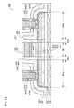

Landscapes
- Thin Film Transistor (AREA)
- Read Only Memory (AREA)
- Semiconductor Memories (AREA)
- Non-Volatile Memory (AREA)
Priority Applications (2)
| Application Number | Priority Date | Filing Date | Title |
|---|---|---|---|
| JP2017123121A JP6975560B2 (ja) | 2017-06-23 | 2017-06-23 | 記憶装置 |
| JP2021181809A JP7225349B2 (ja) | 2017-06-23 | 2021-11-08 | 記憶装置 |
Applications Claiming Priority (1)
| Application Number | Priority Date | Filing Date | Title |
|---|---|---|---|
| JP2017123121A JP6975560B2 (ja) | 2017-06-23 | 2017-06-23 | 記憶装置 |
Related Child Applications (1)
| Application Number | Title | Priority Date | Filing Date |
|---|---|---|---|
| JP2021181809A Division JP7225349B2 (ja) | 2017-06-23 | 2021-11-08 | 記憶装置 |
Publications (3)
| Publication Number | Publication Date |
|---|---|
| JP2019008852A JP2019008852A (ja) | 2019-01-17 |
| JP2019008852A5 JP2019008852A5 (cg-RX-API-DMAC7.html) | 2020-08-13 |
| JP6975560B2 true JP6975560B2 (ja) | 2021-12-01 |
Family
ID=65028953
Family Applications (1)
| Application Number | Title | Priority Date | Filing Date |
|---|---|---|---|
| JP2017123121A Expired - Fee Related JP6975560B2 (ja) | 2017-06-23 | 2017-06-23 | 記憶装置 |
Country Status (1)
| Country | Link |
|---|---|
| JP (1) | JP6975560B2 (cg-RX-API-DMAC7.html) |
Cited By (1)
| Publication number | Priority date | Publication date | Assignee | Title |
|---|---|---|---|---|
| JP2022024001A (ja) * | 2017-06-23 | 2022-02-08 | 株式会社半導体エネルギー研究所 | 記憶装置 |
Families Citing this family (3)
| Publication number | Priority date | Publication date | Assignee | Title |
|---|---|---|---|---|
| JP7480113B2 (ja) * | 2019-02-22 | 2024-05-09 | 株式会社半導体エネルギー研究所 | 半導体装置および当該半導体装置を有する電気機器 |
| TW202431270A (zh) | 2019-03-29 | 2024-08-01 | 日商半導體能源研究所股份有限公司 | 半導體裝置 |
| JP7320227B2 (ja) * | 2019-09-13 | 2023-08-03 | 本田技研工業株式会社 | 半導体装置 |
Family Cites Families (5)
| Publication number | Priority date | Publication date | Assignee | Title |
|---|---|---|---|---|
| JP4654671B2 (ja) * | 2004-11-29 | 2011-03-23 | ソニー株式会社 | 半導体記憶装置 |
| US7310257B2 (en) * | 2005-11-10 | 2007-12-18 | Micron Technology, Inc. | Local digit line architecture and method for memory devices having multi-bit or low capacitance memory cells |
| US7688648B2 (en) * | 2008-09-02 | 2010-03-30 | Juhan Kim | High speed flash memory |
| JP2011040706A (ja) * | 2009-07-15 | 2011-02-24 | Toshiba Corp | 不揮発性半導体記憶装置 |
| JP2015041388A (ja) * | 2013-08-20 | 2015-03-02 | 株式会社半導体エネルギー研究所 | 記憶装置、及び半導体装置 |
-
2017
- 2017-06-23 JP JP2017123121A patent/JP6975560B2/ja not_active Expired - Fee Related
Cited By (2)
| Publication number | Priority date | Publication date | Assignee | Title |
|---|---|---|---|---|
| JP2022024001A (ja) * | 2017-06-23 | 2022-02-08 | 株式会社半導体エネルギー研究所 | 記憶装置 |
| JP7225349B2 (ja) | 2017-06-23 | 2023-02-20 | 株式会社半導体エネルギー研究所 | 記憶装置 |
Also Published As
| Publication number | Publication date |
|---|---|
| JP2019008852A (ja) | 2019-01-17 |
Similar Documents
| Publication | Publication Date | Title |
|---|---|---|
| US11985828B2 (en) | Semiconductor device, semiconductor wafer, memory device, and electronic device | |
| US20240421155A1 (en) | Semiconductor device, semiconductor wafer, memory device, and electronic device | |
| JP7439215B2 (ja) | 半導体装置 | |
| JP7305005B2 (ja) | 記憶装置 | |
| JP6773453B2 (ja) | 記憶装置及び電子機器 | |
| JP7429686B2 (ja) | 半導体装置 | |
| JP6901831B2 (ja) | メモリシステム、及び情報処理システム | |
| WO2020152522A1 (ja) | 半導体装置および当該半導体装置を有する電気機器 | |
| KR102770652B1 (ko) | 감지 증폭기, 반도체 장치, 그 동작 방법, 및 전자 기기 | |
| WO2020170067A1 (ja) | 半導体装置および当該半導体装置を有する電気機器 | |
| JP2023067965A (ja) | 半導体装置 | |
| JP2019008852A (ja) | 記憶装置 | |
| JPWO2018220471A1 (ja) | 記憶装置及びその動作方法 | |
| JP7225349B2 (ja) | 記憶装置 | |
| JP2018206456A (ja) | 記憶装置 | |
| JP7062385B2 (ja) | 記憶装置、及びその動作方法 | |
| WO2018142239A1 (ja) | 半導体装置 | |
| JP7657721B2 (ja) | 半導体装置 | |
| JP7163065B2 (ja) | 半導体装置及び電子機器 | |
| JP2019016681A (ja) | 記憶装置 |
Legal Events
| Date | Code | Title | Description |
|---|---|---|---|
| A521 | Request for written amendment filed |
Free format text: JAPANESE INTERMEDIATE CODE: A523 Effective date: 20200622 |
|
| A621 | Written request for application examination |
Free format text: JAPANESE INTERMEDIATE CODE: A621 Effective date: 20200622 |
|
| A977 | Report on retrieval |
Free format text: JAPANESE INTERMEDIATE CODE: A971007 Effective date: 20210521 |
|
| A131 | Notification of reasons for refusal |
Free format text: JAPANESE INTERMEDIATE CODE: A131 Effective date: 20210601 |
|
| A521 | Request for written amendment filed |
Free format text: JAPANESE INTERMEDIATE CODE: A523 Effective date: 20210727 |
|
| TRDD | Decision of grant or rejection written | ||
| A01 | Written decision to grant a patent or to grant a registration (utility model) |
Free format text: JAPANESE INTERMEDIATE CODE: A01 Effective date: 20211026 |
|
| A61 | First payment of annual fees (during grant procedure) |
Free format text: JAPANESE INTERMEDIATE CODE: A61 Effective date: 20211108 |
|
| R150 | Certificate of patent or registration of utility model |
Ref document number: 6975560 Country of ref document: JP Free format text: JAPANESE INTERMEDIATE CODE: R150 |
|
| R250 | Receipt of annual fees |
Free format text: JAPANESE INTERMEDIATE CODE: R250 |
|
| LAPS | Cancellation because of no payment of annual fees |