JP6956095B2 - 集積回路(ic)パッケージ間にフレキシブルコネクタを備える集積デバイス - Google Patents
集積回路(ic)パッケージ間にフレキシブルコネクタを備える集積デバイス Download PDFInfo
- Publication number
- JP6956095B2 JP6956095B2 JP2018540419A JP2018540419A JP6956095B2 JP 6956095 B2 JP6956095 B2 JP 6956095B2 JP 2018540419 A JP2018540419 A JP 2018540419A JP 2018540419 A JP2018540419 A JP 2018540419A JP 6956095 B2 JP6956095 B2 JP 6956095B2
- Authority
- JP
- Japan
- Prior art keywords
- package
- integrated
- dielectric layer
- michipa
- kkeji
- Prior art date
- Legal status (The legal status is an assumption and is not a legal conclusion. Google has not performed a legal analysis and makes no representation as to the accuracy of the status listed.)
- Active
Links
Images


Classifications
-
- H—ELECTRICITY
- H01—ELECTRIC ELEMENTS
- H01L—SEMICONDUCTOR DEVICES NOT COVERED BY CLASS H10
- H01L23/00—Details of semiconductor or other solid state devices
- H01L23/48—Arrangements for conducting electric current to or from the solid state body in operation, e.g. leads, terminal arrangements ; Selection of materials therefor
- H01L23/488—Arrangements for conducting electric current to or from the solid state body in operation, e.g. leads, terminal arrangements ; Selection of materials therefor consisting of soldered or bonded constructions
- H01L23/498—Leads, i.e. metallisations or lead-frames on insulating substrates, e.g. chip carriers
- H01L23/49833—Leads, i.e. metallisations or lead-frames on insulating substrates, e.g. chip carriers the chip support structure consisting of a plurality of insulating substrates
-
- H—ELECTRICITY
- H01—ELECTRIC ELEMENTS
- H01L—SEMICONDUCTOR DEVICES NOT COVERED BY CLASS H10
- H01L21/00—Processes or apparatus adapted for the manufacture or treatment of semiconductor or solid state devices or of parts thereof
- H01L21/02—Manufacture or treatment of semiconductor devices or of parts thereof
- H01L21/04—Manufacture or treatment of semiconductor devices or of parts thereof the devices having at least one potential-jump barrier or surface barrier, e.g. PN junction, depletion layer or carrier concentration layer
- H01L21/48—Manufacture or treatment of parts, e.g. containers, prior to assembly of the devices, using processes not provided for in a single one of the subgroups H01L21/06 - H01L21/326
- H01L21/4814—Conductive parts
- H01L21/4846—Leads on or in insulating or insulated substrates, e.g. metallisation
- H01L21/4853—Connection or disconnection of other leads to or from a metallisation, e.g. pins, wires, bumps
-
- H—ELECTRICITY
- H01—ELECTRIC ELEMENTS
- H01L—SEMICONDUCTOR DEVICES NOT COVERED BY CLASS H10
- H01L21/00—Processes or apparatus adapted for the manufacture or treatment of semiconductor or solid state devices or of parts thereof
- H01L21/02—Manufacture or treatment of semiconductor devices or of parts thereof
- H01L21/04—Manufacture or treatment of semiconductor devices or of parts thereof the devices having at least one potential-jump barrier or surface barrier, e.g. PN junction, depletion layer or carrier concentration layer
- H01L21/50—Assembly of semiconductor devices using processes or apparatus not provided for in a single one of the subgroups H01L21/06 - H01L21/326, e.g. sealing of a cap to a base of a container
- H01L21/56—Encapsulations, e.g. encapsulation layers, coatings
- H01L21/561—Batch processing
-
- H—ELECTRICITY
- H01—ELECTRIC ELEMENTS
- H01L—SEMICONDUCTOR DEVICES NOT COVERED BY CLASS H10
- H01L21/00—Processes or apparatus adapted for the manufacture or treatment of semiconductor or solid state devices or of parts thereof
- H01L21/02—Manufacture or treatment of semiconductor devices or of parts thereof
- H01L21/04—Manufacture or treatment of semiconductor devices or of parts thereof the devices having at least one potential-jump barrier or surface barrier, e.g. PN junction, depletion layer or carrier concentration layer
- H01L21/50—Assembly of semiconductor devices using processes or apparatus not provided for in a single one of the subgroups H01L21/06 - H01L21/326, e.g. sealing of a cap to a base of a container
- H01L21/56—Encapsulations, e.g. encapsulation layers, coatings
- H01L21/565—Moulds
-
- H—ELECTRICITY
- H01—ELECTRIC ELEMENTS
- H01L—SEMICONDUCTOR DEVICES NOT COVERED BY CLASS H10
- H01L23/00—Details of semiconductor or other solid state devices
- H01L23/28—Encapsulations, e.g. encapsulating layers, coatings, e.g. for protection
- H01L23/29—Encapsulations, e.g. encapsulating layers, coatings, e.g. for protection characterised by the material, e.g. carbon
- H01L23/293—Organic, e.g. plastic
-
- H—ELECTRICITY
- H01—ELECTRIC ELEMENTS
- H01L—SEMICONDUCTOR DEVICES NOT COVERED BY CLASS H10
- H01L23/00—Details of semiconductor or other solid state devices
- H01L23/52—Arrangements for conducting electric current within the device in operation from one component to another, i.e. interconnections, e.g. wires, lead frames
- H01L23/538—Arrangements for conducting electric current within the device in operation from one component to another, i.e. interconnections, e.g. wires, lead frames the interconnection structure between a plurality of semiconductor chips being formed on, or in, insulating substrates
- H01L23/5387—Flexible insulating substrates
-
- H—ELECTRICITY
- H01—ELECTRIC ELEMENTS
- H01L—SEMICONDUCTOR DEVICES NOT COVERED BY CLASS H10
- H01L21/00—Processes or apparatus adapted for the manufacture or treatment of semiconductor or solid state devices or of parts thereof
- H01L21/02—Manufacture or treatment of semiconductor devices or of parts thereof
- H01L21/04—Manufacture or treatment of semiconductor devices or of parts thereof the devices having at least one potential-jump barrier or surface barrier, e.g. PN junction, depletion layer or carrier concentration layer
- H01L21/50—Assembly of semiconductor devices using processes or apparatus not provided for in a single one of the subgroups H01L21/06 - H01L21/326, e.g. sealing of a cap to a base of a container
- H01L21/56—Encapsulations, e.g. encapsulation layers, coatings
- H01L21/568—Temporary substrate used as encapsulation process aid
-
- H—ELECTRICITY
- H01—ELECTRIC ELEMENTS
- H01L—SEMICONDUCTOR DEVICES NOT COVERED BY CLASS H10
- H01L2224/00—Indexing scheme for arrangements for connecting or disconnecting semiconductor or solid-state bodies and methods related thereto as covered by H01L24/00
- H01L2224/01—Means for bonding being attached to, or being formed on, the surface to be connected, e.g. chip-to-package, die-attach, "first-level" interconnects; Manufacturing methods related thereto
- H01L2224/10—Bump connectors; Manufacturing methods related thereto
- H01L2224/15—Structure, shape, material or disposition of the bump connectors after the connecting process
- H01L2224/16—Structure, shape, material or disposition of the bump connectors after the connecting process of an individual bump connector
- H01L2224/161—Disposition
- H01L2224/16151—Disposition the bump connector connecting between a semiconductor or solid-state body and an item not being a semiconductor or solid-state body, e.g. chip-to-substrate, chip-to-passive
- H01L2224/16221—Disposition the bump connector connecting between a semiconductor or solid-state body and an item not being a semiconductor or solid-state body, e.g. chip-to-substrate, chip-to-passive the body and the item being stacked
- H01L2224/16225—Disposition the bump connector connecting between a semiconductor or solid-state body and an item not being a semiconductor or solid-state body, e.g. chip-to-substrate, chip-to-passive the body and the item being stacked the item being non-metallic, e.g. insulating substrate with or without metallisation
- H01L2224/16227—Disposition the bump connector connecting between a semiconductor or solid-state body and an item not being a semiconductor or solid-state body, e.g. chip-to-substrate, chip-to-passive the body and the item being stacked the item being non-metallic, e.g. insulating substrate with or without metallisation the bump connector connecting to a bond pad of the item
-
- H—ELECTRICITY
- H01—ELECTRIC ELEMENTS
- H01L—SEMICONDUCTOR DEVICES NOT COVERED BY CLASS H10
- H01L2224/00—Indexing scheme for arrangements for connecting or disconnecting semiconductor or solid-state bodies and methods related thereto as covered by H01L24/00
- H01L2224/01—Means for bonding being attached to, or being formed on, the surface to be connected, e.g. chip-to-package, die-attach, "first-level" interconnects; Manufacturing methods related thereto
- H01L2224/10—Bump connectors; Manufacturing methods related thereto
- H01L2224/15—Structure, shape, material or disposition of the bump connectors after the connecting process
- H01L2224/16—Structure, shape, material or disposition of the bump connectors after the connecting process of an individual bump connector
- H01L2224/161—Disposition
- H01L2224/16151—Disposition the bump connector connecting between a semiconductor or solid-state body and an item not being a semiconductor or solid-state body, e.g. chip-to-substrate, chip-to-passive
- H01L2224/16221—Disposition the bump connector connecting between a semiconductor or solid-state body and an item not being a semiconductor or solid-state body, e.g. chip-to-substrate, chip-to-passive the body and the item being stacked
- H01L2224/16225—Disposition the bump connector connecting between a semiconductor or solid-state body and an item not being a semiconductor or solid-state body, e.g. chip-to-substrate, chip-to-passive the body and the item being stacked the item being non-metallic, e.g. insulating substrate with or without metallisation
- H01L2224/16238—Disposition the bump connector connecting between a semiconductor or solid-state body and an item not being a semiconductor or solid-state body, e.g. chip-to-substrate, chip-to-passive the body and the item being stacked the item being non-metallic, e.g. insulating substrate with or without metallisation the bump connector connecting to a bonding area protruding from the surface of the item
-
- H—ELECTRICITY
- H01—ELECTRIC ELEMENTS
- H01L—SEMICONDUCTOR DEVICES NOT COVERED BY CLASS H10
- H01L2224/00—Indexing scheme for arrangements for connecting or disconnecting semiconductor or solid-state bodies and methods related thereto as covered by H01L24/00
- H01L2224/01—Means for bonding being attached to, or being formed on, the surface to be connected, e.g. chip-to-package, die-attach, "first-level" interconnects; Manufacturing methods related thereto
- H01L2224/26—Layer connectors, e.g. plate connectors, solder or adhesive layers; Manufacturing methods related thereto
- H01L2224/31—Structure, shape, material or disposition of the layer connectors after the connecting process
- H01L2224/32—Structure, shape, material or disposition of the layer connectors after the connecting process of an individual layer connector
- H01L2224/321—Disposition
- H01L2224/32151—Disposition the layer connector connecting between a semiconductor or solid-state body and an item not being a semiconductor or solid-state body, e.g. chip-to-substrate, chip-to-passive
- H01L2224/32221—Disposition the layer connector connecting between a semiconductor or solid-state body and an item not being a semiconductor or solid-state body, e.g. chip-to-substrate, chip-to-passive the body and the item being stacked
- H01L2224/32225—Disposition the layer connector connecting between a semiconductor or solid-state body and an item not being a semiconductor or solid-state body, e.g. chip-to-substrate, chip-to-passive the body and the item being stacked the item being non-metallic, e.g. insulating substrate with or without metallisation
-
- H—ELECTRICITY
- H01—ELECTRIC ELEMENTS
- H01L—SEMICONDUCTOR DEVICES NOT COVERED BY CLASS H10
- H01L2224/00—Indexing scheme for arrangements for connecting or disconnecting semiconductor or solid-state bodies and methods related thereto as covered by H01L24/00
- H01L2224/73—Means for bonding being of different types provided for in two or more of groups H01L2224/10, H01L2224/18, H01L2224/26, H01L2224/34, H01L2224/42, H01L2224/50, H01L2224/63, H01L2224/71
- H01L2224/732—Location after the connecting process
- H01L2224/73201—Location after the connecting process on the same surface
- H01L2224/73203—Bump and layer connectors
- H01L2224/73204—Bump and layer connectors the bump connector being embedded into the layer connector
-
- H—ELECTRICITY
- H01—ELECTRIC ELEMENTS
- H01L—SEMICONDUCTOR DEVICES NOT COVERED BY CLASS H10
- H01L2224/00—Indexing scheme for arrangements for connecting or disconnecting semiconductor or solid-state bodies and methods related thereto as covered by H01L24/00
- H01L2224/91—Methods for connecting semiconductor or solid state bodies including different methods provided for in two or more of groups H01L2224/80 - H01L2224/90
- H01L2224/92—Specific sequence of method steps
- H01L2224/921—Connecting a surface with connectors of different types
- H01L2224/9212—Sequential connecting processes
- H01L2224/92122—Sequential connecting processes the first connecting process involving a bump connector
- H01L2224/92125—Sequential connecting processes the first connecting process involving a bump connector the second connecting process involving a layer connector
-
- H—ELECTRICITY
- H01—ELECTRIC ELEMENTS
- H01L—SEMICONDUCTOR DEVICES NOT COVERED BY CLASS H10
- H01L23/00—Details of semiconductor or other solid state devices
- H01L23/28—Encapsulations, e.g. encapsulating layers, coatings, e.g. for protection
- H01L23/31—Encapsulations, e.g. encapsulating layers, coatings, e.g. for protection characterised by the arrangement or shape
- H01L23/3107—Encapsulations, e.g. encapsulating layers, coatings, e.g. for protection characterised by the arrangement or shape the device being completely enclosed
- H01L23/3121—Encapsulations, e.g. encapsulating layers, coatings, e.g. for protection characterised by the arrangement or shape the device being completely enclosed a substrate forming part of the encapsulation
-
- H—ELECTRICITY
- H01—ELECTRIC ELEMENTS
- H01L—SEMICONDUCTOR DEVICES NOT COVERED BY CLASS H10
- H01L25/00—Assemblies consisting of a plurality of individual semiconductor or other solid state devices ; Multistep manufacturing processes thereof
- H01L25/03—Assemblies consisting of a plurality of individual semiconductor or other solid state devices ; Multistep manufacturing processes thereof all the devices being of a type provided for in the same subgroup of groups H01L27/00 - H01L33/00, or in a single subclass of H10K, H10N, e.g. assemblies of rectifier diodes
- H01L25/04—Assemblies consisting of a plurality of individual semiconductor or other solid state devices ; Multistep manufacturing processes thereof all the devices being of a type provided for in the same subgroup of groups H01L27/00 - H01L33/00, or in a single subclass of H10K, H10N, e.g. assemblies of rectifier diodes the devices not having separate containers
- H01L25/065—Assemblies consisting of a plurality of individual semiconductor or other solid state devices ; Multistep manufacturing processes thereof all the devices being of a type provided for in the same subgroup of groups H01L27/00 - H01L33/00, or in a single subclass of H10K, H10N, e.g. assemblies of rectifier diodes the devices not having separate containers the devices being of a type provided for in group H01L27/00
- H01L25/0652—Assemblies consisting of a plurality of individual semiconductor or other solid state devices ; Multistep manufacturing processes thereof all the devices being of a type provided for in the same subgroup of groups H01L27/00 - H01L33/00, or in a single subclass of H10K, H10N, e.g. assemblies of rectifier diodes the devices not having separate containers the devices being of a type provided for in group H01L27/00 the devices being arranged next and on each other, i.e. mixed assemblies
-
- H—ELECTRICITY
- H01—ELECTRIC ELEMENTS
- H01L—SEMICONDUCTOR DEVICES NOT COVERED BY CLASS H10
- H01L2924/00—Indexing scheme for arrangements or methods for connecting or disconnecting semiconductor or solid-state bodies as covered by H01L24/00
- H01L2924/15—Details of package parts other than the semiconductor or other solid state devices to be connected
- H01L2924/181—Encapsulation
- H01L2924/1815—Shape
Description
本出願は、その内容全体が参照により本明細書に組み込まれる、2016年2月10日に米国特許商標庁に出願された、非仮出願第15/040,881号の優先権および利益を主張する。
図2は、第1のパッケージ202(たとえば、第1の集積回路(IC)パッケージ)と、第2のパッケージ204(たとえば、第2の集積回路(IC)パッケージ)と、フレキシブルコネクタ206(たとえば、2つのパッケージ同士を電気的に接続するための手段)とを含む集積デバイス200(たとえば、集積回路(IC)デバイス)を示す。第1のパッケージ202は、フレキシブルコネクタ206を介して第2のパッケージ204に結合される。以下でさらに説明するように、フレキシブルコネクタ206は、第1のパッケージ202を第2のパッケージ204に電気的および/または機械的に結合するように構成される。
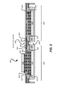
図3は、第1のパッケージ202(たとえば、第1の集積回路(IC)パッケージ)と、第2のパッケージ304(たとえば、第2の集積回路(IC)パッケージ)と、フレキシブルコネクタ206(たとえば、2つのパッケージ同士を電気的に接続するための手段)とを含む集積デバイス300(たとえば、集積回路(IC)デバイス)を示す。第1のパッケージ202は、フレキシブルコネクタ206を介して第2のパッケージ304に結合される。フレキシブルコネクタ206は、第1のパッケージ202を第2のパッケージ304に電気的に結合するように構成される。
図4は、第1のパッケージ202(たとえば、第1の集積回路(IC)パッケージ)と、第2のパッケージ404(たとえば、第2の集積回路(IC)パッケージ)と、フレキシブルコネクタ206とを含む集積デバイス400(たとえば、集積回路(IC)デバイス)を示す。第1のパッケージ202は、フレキシブルコネクタ206(たとえば、2つのパッケージ同士を電気的に接続するための手段)を介して第2のパッケージ404に結合される。フレキシブルコネクタ206は、第1のパッケージ202を第2のパッケージ404に電気的に結合するように構成される。
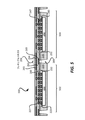
図5は、第1のパッケージ502(たとえば、第1の集積回路(IC)パッケージ)と、第2のパッケージ504(たとえば、第2の集積回路(IC)パッケージ)と、フレキシブルコネクタ206とを含む集積デバイス500(たとえば、集積回路(IC)デバイス)を示す。第1のパッケージ202は、フレキシブルコネクタ206(たとえば、2つのパッケージ同士を電気的に接続するための手段)を介して第2のパッケージ504に結合される。フレキシブルコネクタ206は、第1のパッケージ502を第2のパッケージ504に電気的に結合するように構成される。
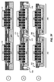
いくつかの実装形態では、埋込み型フレキシブルコネクタを含む集積回路(IC)デバイスを設ける/製作することは、いくつかのプロセスを含む。図7(図7A〜図7Fを含む)は、埋込み型フレキシブルコネクタを含む集積回路(IC)デバイスを設ける/製作するための例示的なシーケンスを示す。いくつかの実装形態では、図7A〜図7Fのシーケンスは、図2の埋込み型フレキシブルコネクタを含む集積回路(IC)デバイスおよび/または本開示において説明する他の集積回路(IC)デバイスを製作するために使用される場合がある。次に、図7A〜図7Fについて、図2の集積回路(IC)デバイスを設ける/製作する状況において説明する。
いくつかの実装形態では、埋込み型フレキシブルコネクタを含む集積回路(IC)デバイスを設ける/製作することは、いくつかのプロセスを含む。図8は、埋込み型フレキシブルコネクタを含む集積回路(IC)デバイスを設ける/製作するための方法800の例示的な流れ図を示す。いくつかの実装形態では、図8の方法は、図2〜図6の埋込み型フレキシブルコネクタを含む集積回路(IC)デバイスおよび/または本開示において説明する他の集積回路(IC)デバイスを製作するために使用される場合がある。図8について、図2の集積回路(IC)デバイスを製作する状況において説明する。
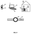
図9は、上述の集積デバイス、半導体デバイス、集積回路、ダイ、インターポーザ、パッケージ、またはパッケージオンパッケージ(PoP)のいずれかと統合されることがある様々な電子デバイスを示す。たとえば、モバイル電話デバイス902、ラップトップコンピュータデバイス904、固定ロケーション端末デバイス906、ウェアラブルデバイス908が、本明細書で説明するような集積デバイス900を含んでよい。集積デバイス900は、たとえば、本明細書で説明する集積回路、ダイ、集積デバイス、集積デバイスパッケージ、集積回路デバイス、デバイスパッケージ、集積回路(IC)パッケージ、パッケージオンパッケージデバイスのいずれかであってよい。図9に示すデバイス902、904、906、908は、例にすぎない。他の電子デバイスも、限定はしないが、モバイルデバイス、ハンドヘルドパーソナル通信システム(PCS)ユニット、携帯情報端末などのポータブルデータユニット、全地球測位システム(GPS)対応デバイス、ナビゲーションデバイス、セットトップボックス、音楽プレーヤ、ビデオプレーヤ、エンターテイメントユニット、メーター読取り機器などの固定ロケーションデータユニット、通信デバイス、スマートフォン、タブレットコンピュータ、コンピュータ、ウェアラブルデバイス(たとえば、時計、眼鏡)、モノのインターネット(IoT)デバイス、サーバ、ルータ、自動車車両(たとえば、自律車両)に実装された電子デバイス、またはデータもしくはコンピュータ命令を記憶しもしくは取り出す任意の他のデバイス、あるいはそれらの任意の組合せを含むデバイス(たとえば、電子デバイス)のグループを含む、集積デバイス900を特徴として備えてもよい。
102 第1の集積回路(IC)パッケージ
104 第2の集積回路(IC)パッケージ
106 フレキシブルコネクタ
120 プリント回路板(PCB)
122 第1のチップ
140 プリント回路板(PCB)
160 配線
162 第1のPCBインターフェース
164 第2のPCBインターフェース
166 カバー
200 集積デバイス
202 第1のパッケージ
204 第2のパッケージ
206 フレキシブルコネクタ
209 キャビティ
220 第1の誘電体層
222 第1のダイ
223 第1の相互接続部
224 第2のダイ
225 第1の相互接続部
227 第1の相互接続部
232 アンダーフィル
234 アンダーフィル
240 第2のパッケージ
242 第3のダイ
243 第1の相互接続部
244 第4のダイ
245 相互接続部
247 第1の相互接続部
252 アンダーフィル
254 アンダーフィル
260 第2の誘電体層
262 第3の誘電体層
264 はんだレジスト層
265 相互接続部
269 ダミー金属層
300 集積デバイス
304 第2のパッケージ
400 集積デバイス
404 第2のパッケージ
500 集積デバイス
502 第1のパッケージ
504 第2のパッケージ
600 集積デバイス
606 フレキシブルコネクタ
700 キャリア
702 キャビティ
703 相互接続部
704 キャビティ
707 相互接続部
709 キャビティ
710 シード層
720 積層
730 積層
731 キャビティ
733 相互接続部
735 キャビティ
737 相互接続部
743 キャビティ
745 キャビティ
750 積層
753 相互接続部
757 相互接続部
763 相互接続部
767 相互接続部
900 集積デバイス
902 モバイル電話デバイス
904 ラップトップコンピュータデバイス
906 固定ロケーション端末デバイス
908 ウェアラブルデバイス
Claims (15)
- 集積デバイスであって、
第1の集積回路パッケージであって、
第1のダイと、
複数の第1の相互接続部と、
前記第1のダイを封入する誘電体層と
を備える第1の集積回路パッケージと、
前記第1の集積回路パッケージに結合されたフレキシブルコネクタであって、
前記誘電体層と、
ダミー金属層と、
相互接続部と
を備え、前記誘電体層は、キャビティを含み、前記ダミー金属層は、レーザが前記誘電体層の一部を貫通するのを妨げるように構成されている、フレキシブルコネクタと、
前記フレキシブルコネクタに結合された第2の集積回路パッケージであって、
前記誘電体層と、
複数の第2の相互接続部と
を備える第2の集積回路パッケージとを備え、
前記第1の集積回路パッケージ、前記第2の集積回路パッケージ、および前記フレキシブルコネクタは、前記誘電体層の少なくとも一部を介して互いに結合される集積デバイス。 - 前記第1の集積回路パッケージ、前記第2の集積回路パッケージ、および前記フレキシブルコネクタによって共有される前記誘電体層の前記一部は、前記誘電体層の連続部分を共有している、請求項1に記載の集積デバイス。
- 前記ダミー金属層は、電気信号を送信しないように構成される、請求項1に記載の集積デバイス。
- 前記第2の集積回路パッケージは、前記誘電体層内に位置する第2のダイ、または前記誘電体層の上方に位置する第2のダイを備える、請求項1に記載の集積デバイス。
- 前記第1の集積回路パッケージは、前記誘電体層の上方に位置する第2のダイを備える、請求項1に記載の集積デバイス。
- 前記第1のダイは第1のダイパッケージであり、前記第2のダイは第2のダイパッケージであり、前記第1の集積回路パッケージはパッケージオンパッケージデバイスを備える、請求項5に記載の集積デバイス。
- 前記誘電体層はポリイミド層を含む、請求項1に記載の集積デバイス。
- 前記誘電体層は複数の誘電体層を備える、請求項1に記載の集積デバイス。
- 前記フレキシブルコネクタはパッケージツーパッケージコネクタである、請求項1に記載の集積デバイス。
- 前記集積デバイスは、音楽プレーヤ、ビデオプレーヤ、エンターテイメントユニット、ナビゲーションデバイス、通信デバイス、モバイルデバイス、モバイルフォン、スマートフォン、携帯情報端末、固定ロケーション端末、タブレットコンピュータ、コンピュータ、ウェアラブルデバイス、モノのインターネットデバイス、ラップトップコンピュータ、サーバ、および自動車車両の中のデバイスからなる群から選択されたデバイスの中に組み込まれる、請求項1に記載の集積デバイス。
- 集積デバイスを製作するための方法であって、
誘電体層を形成するステップと、
第1の集積回路パッケージを設けるステップであって、
第1のダイを設けるステップと、
複数の第1の相互接続部を形成するステップと、
を含み、前記誘電体層は前記第1のダイを封入する、第1の集積回路パッケージを設けるステップと、
第2の集積回路パッケージを設けるステップであって、
複数の第2の相互接続部を形成するステップと
を含む、第2の集積回路パッケージを設けるステップと、
フレキシブルコネクタを、前記第1の集積回路パッケージおよび前記第2の集積回路パッケージに結合されるように形成するステップであって、
相互接続部を形成するステップと、
前記誘電体層にダミー金属層を形成するステップと、
レーザプロセスを使用して前記誘電体層にキャビティを作製するステップであって、前記ダミー金属層は、レーザが前記誘電体層の一部を貫通するのを妨げるように構成されている、キャビティを作製するステップと
を含む、フレキシブルコネクタを形成するステップとを含み
前記第1の集積回路パッケージ、前記第2の集積回路パッケージ、および前記フレキシブルコネクタは、前記第1の集積回路パッケージ、前記第2の集積回路パッケージ、および前記フレキシブルコネクタが前記誘電体層の少なくとも一部を介して互いに結合されるように形成される方法。 - 前記第1の集積回路パッケージ、前記第2の集積回路パッケージ、および前記フレキシブルコネクタによって共有される前記誘電体層の前記一部は、前記誘電体層の連続部分を共有している、請求項11に記載の方法。
- 前記ダミー金属層は、電気信号を送信しないように構成される、請求項11に記載の方法。
- 前記誘電体層を形成するステップは、ポリイミド層を形成するステップを含む、請求項11に記載の方法。
- 前記フレキシブルコネクタは、電気信号が、プリント回路板をバイパスしつつ、前記第1の集積回路パッケージと前記第2の集積回路パッケージとの間を移動するのを可能にするように構成される、請求項11に記載の方法。
Applications Claiming Priority (3)
| Application Number | Priority Date | Filing Date | Title |
|---|---|---|---|
| US15/040,881 US9633950B1 (en) | 2016-02-10 | 2016-02-10 | Integrated device comprising flexible connector between integrated circuit (IC) packages |
| US15/040,881 | 2016-02-10 | ||
| PCT/US2017/016864 WO2017139285A1 (en) | 2016-02-10 | 2017-02-07 | Integrated device comprising flexible connector between integrated circuit (ic) packages |
Publications (3)
| Publication Number | Publication Date |
|---|---|
| JP2019510368A JP2019510368A (ja) | 2019-04-11 |
| JP2019510368A5 JP2019510368A5 (ja) | 2020-02-27 |
| JP6956095B2 true JP6956095B2 (ja) | 2021-10-27 |
Family
ID=58057302
Family Applications (1)
| Application Number | Title | Priority Date | Filing Date |
|---|---|---|---|
| JP2018540419A Active JP6956095B2 (ja) | 2016-02-10 | 2017-02-07 | 集積回路(ic)パッケージ間にフレキシブルコネクタを備える集積デバイス |
Country Status (9)
| Country | Link |
|---|---|
| US (1) | US9633950B1 (ja) |
| EP (1) | EP3414776B1 (ja) |
| JP (1) | JP6956095B2 (ja) |
| KR (1) | KR20180111840A (ja) |
| CN (1) | CN108604585B (ja) |
| AU (1) | AU2017217375A1 (ja) |
| BR (1) | BR112018016132B1 (ja) |
| TW (1) | TWI601217B (ja) |
| WO (1) | WO2017139285A1 (ja) |
Families Citing this family (3)
| Publication number | Priority date | Publication date | Assignee | Title |
|---|---|---|---|---|
| US11581261B2 (en) * | 2018-06-12 | 2023-02-14 | Novatek Microelectronics Corp. | Chip on film package |
| US11342268B2 (en) * | 2020-01-29 | 2022-05-24 | Amkor Technology Singapore Holding Pte. Ltd. | Semiconductor devices and methods of manufacturing semiconductor devices |
| US20220157680A1 (en) * | 2020-11-19 | 2022-05-19 | Apple Inc. | Flexible Package Architecture Concept in Fanout |
Family Cites Families (22)
| Publication number | Priority date | Publication date | Assignee | Title |
|---|---|---|---|---|
| US4246595A (en) * | 1977-03-08 | 1981-01-20 | Matsushita Electric Industrial Co., Ltd. | Electronics circuit device and method of making the same |
| JP3280394B2 (ja) * | 1990-04-05 | 2002-05-13 | ロックヒード マーティン コーポレーション | 電子装置 |
| US5527741A (en) * | 1994-10-11 | 1996-06-18 | Martin Marietta Corporation | Fabrication and structures of circuit modules with flexible interconnect layers |
| CN1186971C (zh) | 1999-04-22 | 2005-01-26 | 罗姆股份有限公司 | 印刷电路板、电池组件和印刷电路板的制造方法 |
| FR2793352B1 (fr) | 1999-05-07 | 2006-09-22 | Sagem | Composant electrique a nappe souple de conducteurs de raccordement |
| US6940729B2 (en) | 2001-10-26 | 2005-09-06 | Staktek Group L.P. | Integrated circuit stacking system and method |
| JP2006502587A (ja) | 2002-10-11 | 2006-01-19 | テッセラ,インコーポレイテッド | マルチチップパッケージ用のコンポーネント、方法およびアセンブリ |
| US6862191B1 (en) * | 2003-08-19 | 2005-03-01 | Cardiac Pacemakers, Inc. | Volumetrically efficient electronic circuit module |
| US20060033217A1 (en) * | 2004-08-10 | 2006-02-16 | Brian Taggart | Flip-chips on flex substrates, flip-chip and wire-bonded chip stacks, and methods of assembling same |
| KR100659826B1 (ko) | 2005-12-20 | 2006-12-19 | 삼성에스디아이 주식회사 | 배터리 팩의 회로 기판 |
| DE102006004321A1 (de) * | 2006-01-31 | 2007-08-16 | Häusermann GmbH | Biegbare Leiterplatte mit zusätzlichem funktionalem Element und einer Kerbfräsung und Herstellverfahren und Anwendung |
| JP2010504571A (ja) | 2006-09-19 | 2010-02-12 | イビデン株式会社 | 光インターコネクトデバイス及びその製造方法 |
| US8031475B2 (en) * | 2007-07-12 | 2011-10-04 | Stats Chippac, Ltd. | Integrated circuit package system with flexible substrate and mounded package |
| TWI365524B (en) * | 2007-10-04 | 2012-06-01 | Unimicron Technology Corp | Stackable semiconductor device and fabrication method thereof |
| JP4975584B2 (ja) * | 2007-10-26 | 2012-07-11 | ルネサスエレクトロニクス株式会社 | 半導体装置及び半導体装置の製造方法。 |
| KR20090078124A (ko) * | 2008-01-14 | 2009-07-17 | 한국광기술원 | 연성 광전배선을 이용한 시스템 패키지 및 그의 신호 처리방법 |
| FI122216B (fi) * | 2009-01-05 | 2011-10-14 | Imbera Electronics Oy | Rigid-flex moduuli |
| US20110194240A1 (en) * | 2010-02-05 | 2011-08-11 | Broadcom Corporation | Waveguide assembly and applications thereof |
| KR101078743B1 (ko) | 2010-04-14 | 2011-11-02 | 주식회사 하이닉스반도체 | 스택 패키지 |
| US9190380B2 (en) * | 2012-12-06 | 2015-11-17 | Intel Corporation | High density substrate routing in BBUL package |
| JP2014192476A (ja) | 2013-03-28 | 2014-10-06 | Fujitsu Ltd | プリント基板の半田実装方法及び半田実装構造 |
| KR102135415B1 (ko) | 2013-06-28 | 2020-07-17 | 엘지이노텍 주식회사 | 회로기판 및 상기 회로기판을 포함하는 조명장치 |
-
2016
- 2016-02-10 US US15/040,881 patent/US9633950B1/en active Active
-
2017
- 2017-02-06 TW TW106103767A patent/TWI601217B/zh active
- 2017-02-07 CN CN201780010368.8A patent/CN108604585B/zh active Active
- 2017-02-07 EP EP17706067.0A patent/EP3414776B1/en active Active
- 2017-02-07 AU AU2017217375A patent/AU2017217375A1/en not_active Abandoned
- 2017-02-07 WO PCT/US2017/016864 patent/WO2017139285A1/en active Application Filing
- 2017-02-07 BR BR112018016132-2A patent/BR112018016132B1/pt active IP Right Grant
- 2017-02-07 JP JP2018540419A patent/JP6956095B2/ja active Active
- 2017-02-07 KR KR1020187022909A patent/KR20180111840A/ko not_active Application Discontinuation
Also Published As
| Publication number | Publication date |
|---|---|
| KR20180111840A (ko) | 2018-10-11 |
| CN108604585B (zh) | 2021-09-24 |
| EP3414776A1 (en) | 2018-12-19 |
| TWI601217B (zh) | 2017-10-01 |
| US9633950B1 (en) | 2017-04-25 |
| CN108604585A (zh) | 2018-09-28 |
| BR112018016132A2 (pt) | 2019-01-02 |
| TW201735193A (zh) | 2017-10-01 |
| JP2019510368A (ja) | 2019-04-11 |
| AU2017217375A1 (en) | 2018-07-26 |
| EP3414776B1 (en) | 2021-06-16 |
| WO2017139285A1 (en) | 2017-08-17 |
| BR112018016132B1 (pt) | 2022-09-20 |
Similar Documents
| Publication | Publication Date | Title |
|---|---|---|
| TWI780357B (zh) | 印刷電路板裝置 | |
| US9633977B1 (en) | Integrated device comprising flexible connector between integrated circuit (IC) packages | |
| US9642259B2 (en) | Embedded bridge structure in a substrate | |
| US9349708B2 (en) | Chip stacked package structure and electronic device | |
| KR20190107985A (ko) | 팬-아웃 반도체 패키지 | |
| CN107735860B (zh) | 包括电容器、重分布层、和分立同轴连接的封装基板 | |
| US20120049366A1 (en) | Package structure having through-silicon-via (tsv) chip embedded therein and fabrication method thereof | |
| JP6980530B2 (ja) | 相互接続のスタックと、はんだレジスト層上の相互接続と、基板の側面部分上の相互接続とを備える基板 | |
| US9299602B2 (en) | Enabling package-on-package (PoP) pad surface finishes on bumpless build-up layer (BBUL) package | |
| CN107534041B (zh) | 包括集成电路器件封装之间的焊料连接的层叠封装(PoP)器件 | |
| JP2019528568A (ja) | スイッチおよびフィルタを備えるパッケージ | |
| JP6275670B2 (ja) | 高密度チップ間接続 | |
| US20160343646A1 (en) | High aspect ratio interconnect for wafer level package (wlp) and integrated circuit (ic) package | |
| JP6956095B2 (ja) | 集積回路(ic)パッケージ間にフレキシブルコネクタを備える集積デバイス | |
| US9355898B2 (en) | Package on package (PoP) integrated device comprising a plurality of solder resist layers | |
| WO2018175099A1 (en) | Low profile integrated package | |
| US9799628B2 (en) | Stacked package configurations and methods of making the same | |
| TW202117996A (zh) | 包括具有內部互連、介電層和傳導層的互連結構的整合元件 | |
| CN107112310B (zh) | 包括高性能封装间连接的层叠封装(pop)器件 | |
| CN112635439A (zh) | 具有预制的铁氧体芯的同轴磁感应器 | |
| CN115362550A (zh) | 包括具有在阻焊层之上的互连路由线路的基板的封装件 | |
| JP2024505487A (ja) | 基板の表面と整合された表面相互接続を備える基板を有するパッケージ | |
| TWI658553B (zh) | 扇出型半導體封裝 | |
| EP2962535B1 (en) | Package substrate with testing pads on fine pitch traces | |
| US20210057397A1 (en) | Electrodeless passive embedded substrate |
Legal Events
| Date | Code | Title | Description |
|---|---|---|---|
| A521 | Request for written amendment filed |
Free format text: JAPANESE INTERMEDIATE CODE: A523 Effective date: 20180813 |
|
| A521 | Request for written amendment filed |
Free format text: JAPANESE INTERMEDIATE CODE: A523 Effective date: 20200116 |
|
| A621 | Written request for application examination |
Free format text: JAPANESE INTERMEDIATE CODE: A621 Effective date: 20200116 |
|
| A977 | Report on retrieval |
Free format text: JAPANESE INTERMEDIATE CODE: A971007 Effective date: 20200929 |
|
| A131 | Notification of reasons for refusal |
Free format text: JAPANESE INTERMEDIATE CODE: A131 Effective date: 20201109 |
|
| TRDD | Decision of grant or rejection written | ||
| A01 | Written decision to grant a patent or to grant a registration (utility model) |
Free format text: JAPANESE INTERMEDIATE CODE: A01 Effective date: 20210906 |
|
| A61 | First payment of annual fees (during grant procedure) |
Free format text: JAPANESE INTERMEDIATE CODE: A61 Effective date: 20211004 |
|
| R150 | Certificate of patent or registration of utility model |
Ref document number: 6956095 Country of ref document: JP Free format text: JAPANESE INTERMEDIATE CODE: R150 |