EP2962535B1 - Package substrate with testing pads on fine pitch traces - Google Patents
Package substrate with testing pads on fine pitch traces Download PDFInfo
- Publication number
- EP2962535B1 EP2962535B1 EP14711635.4A EP14711635A EP2962535B1 EP 2962535 B1 EP2962535 B1 EP 2962535B1 EP 14711635 A EP14711635 A EP 14711635A EP 2962535 B1 EP2962535 B1 EP 2962535B1
- Authority
- EP
- European Patent Office
- Prior art keywords
- substrate
- traces
- resist layer
- solder resist
- testing
- Prior art date
- Legal status (The legal status is an assumption and is not a legal conclusion. Google has not performed a legal analysis and makes no representation as to the accuracy of the status listed.)
- Active
Links
Images


Classifications
-
- H—ELECTRICITY
- H05—ELECTRIC TECHNIQUES NOT OTHERWISE PROVIDED FOR
- H05K—PRINTED CIRCUITS; CASINGS OR CONSTRUCTIONAL DETAILS OF ELECTRIC APPARATUS; MANUFACTURE OF ASSEMBLAGES OF ELECTRICAL COMPONENTS
- H05K1/00—Printed circuits
- H05K1/02—Details
- H05K1/11—Printed elements for providing electric connections to or between printed circuits
- H05K1/111—Pads for surface mounting, e.g. lay-out
-
- G—PHYSICS
- G01—MEASURING; TESTING
- G01R—MEASURING ELECTRIC VARIABLES; MEASURING MAGNETIC VARIABLES
- G01R31/00—Arrangements for testing electric properties; Arrangements for locating electric faults; Arrangements for electrical testing characterised by what is being tested not provided for elsewhere
- G01R31/28—Testing of electronic circuits, e.g. by signal tracer
- G01R31/2801—Testing of printed circuits, backplanes, motherboards, hybrid circuits or carriers for multichip packages [MCP]
- G01R31/2818—Testing of printed circuits, backplanes, motherboards, hybrid circuits or carriers for multichip packages [MCP] using test structures on, or modifications of, the card under test, made for the purpose of testing, e.g. additional components or connectors
-
- H—ELECTRICITY
- H05—ELECTRIC TECHNIQUES NOT OTHERWISE PROVIDED FOR
- H05K—PRINTED CIRCUITS; CASINGS OR CONSTRUCTIONAL DETAILS OF ELECTRIC APPARATUS; MANUFACTURE OF ASSEMBLAGES OF ELECTRICAL COMPONENTS
- H05K1/00—Printed circuits
- H05K1/02—Details
- H05K1/0266—Marks, test patterns or identification means
- H05K1/0268—Marks, test patterns or identification means for electrical inspection or testing
-
- H—ELECTRICITY
- H05—ELECTRIC TECHNIQUES NOT OTHERWISE PROVIDED FOR
- H05K—PRINTED CIRCUITS; CASINGS OR CONSTRUCTIONAL DETAILS OF ELECTRIC APPARATUS; MANUFACTURE OF ASSEMBLAGES OF ELECTRICAL COMPONENTS
- H05K3/00—Apparatus or processes for manufacturing printed circuits
- H05K3/30—Assembling printed circuits with electric components, e.g. with resistor
- H05K3/32—Assembling printed circuits with electric components, e.g. with resistor electrically connecting electric components or wires to printed circuits
- H05K3/34—Assembling printed circuits with electric components, e.g. with resistor electrically connecting electric components or wires to printed circuits by soldering
- H05K3/3452—Solder masks
-
- H—ELECTRICITY
- H05—ELECTRIC TECHNIQUES NOT OTHERWISE PROVIDED FOR
- H05K—PRINTED CIRCUITS; CASINGS OR CONSTRUCTIONAL DETAILS OF ELECTRIC APPARATUS; MANUFACTURE OF ASSEMBLAGES OF ELECTRICAL COMPONENTS
- H05K2201/00—Indexing scheme relating to printed circuits covered by H05K1/00
- H05K2201/10—Details of components or other objects attached to or integrated in a printed circuit board
- H05K2201/10613—Details of electrical connections of non-printed components, e.g. special leads
- H05K2201/10621—Components characterised by their electrical contacts
- H05K2201/10674—Flip chip
-
- Y—GENERAL TAGGING OF NEW TECHNOLOGICAL DEVELOPMENTS; GENERAL TAGGING OF CROSS-SECTIONAL TECHNOLOGIES SPANNING OVER SEVERAL SECTIONS OF THE IPC; TECHNICAL SUBJECTS COVERED BY FORMER USPC CROSS-REFERENCE ART COLLECTIONS [XRACs] AND DIGESTS
- Y10—TECHNICAL SUBJECTS COVERED BY FORMER USPC
- Y10T—TECHNICAL SUBJECTS COVERED BY FORMER US CLASSIFICATION
- Y10T29/00—Metal working
- Y10T29/49—Method of mechanical manufacture
- Y10T29/49002—Electrical device making
- Y10T29/49004—Electrical device making including measuring or testing of device or component part
-
- Y—GENERAL TAGGING OF NEW TECHNOLOGICAL DEVELOPMENTS; GENERAL TAGGING OF CROSS-SECTIONAL TECHNOLOGIES SPANNING OVER SEVERAL SECTIONS OF THE IPC; TECHNICAL SUBJECTS COVERED BY FORMER USPC CROSS-REFERENCE ART COLLECTIONS [XRACs] AND DIGESTS
- Y10—TECHNICAL SUBJECTS COVERED BY FORMER USPC
- Y10T—TECHNICAL SUBJECTS COVERED BY FORMER US CLASSIFICATION
- Y10T29/00—Metal working
- Y10T29/49—Method of mechanical manufacture
- Y10T29/49002—Electrical device making
- Y10T29/49117—Conductor or circuit manufacturing
- Y10T29/49124—On flat or curved insulated base, e.g., printed circuit, etc.
- Y10T29/4913—Assembling to base an electrical component, e.g., capacitor, etc.
Definitions
- Various features relate to a package substrate with testing pads on fine pitch traces.
- thermal compression bonding process is a process used to assemble / package a flip chip, die or semiconductor device to a package substrate. Such a flip chip is often referred to as a thermal compression flip chip (TCFC).
- Thermal compression bonding processes provide several advantages over traditional bonding processes. For example, thermal compression bonding processes are generally more accurate than other solder bonding processes. Thus, thermal compression bonding processes are ideal when using fine pitch traces on a substrate (e.g., less than 100 microns ( ⁇ m)). In contrast, other solder bonding processes are limited to a bonding pitch that is greater than 100 microns ( ⁇ m). Thus, TCFCs are typically higher density chips than chips using other bonding processes.
- FIG. 1 illustrates such an example.
- FIG. 1 conceptually illustrates a package substrate 100 that includes several fine pitch traces 102.
- FIG. 1 also illustrates several testing pins 104 being electrically coupled to the traces 102. As shown in FIG. 1 , the testing pins 104 are not aligned with the traces 102. The result of this misalignment is that the package substrate may not be properly tested.
- a printed wiring board comprising an insulating substrate having a mounting surface, a recognition mark formed on the mounting surface of the insulating substrate, and a plurality of reinforcing patterns formed on the mounting surface of the insulating substrate.
- the reinforcing patterns extend from an outer periphery of the recognition mark toward outside of the recognition mark and are arranged circumferentially at intervals relative to the recognition mark.
- Each of the reinforcing patterns has a width less than a width of a part of the outer periphery of the recognition mark connecting adjacent ones of the reinforcing patterns.
- circuit substrate provided with a plurality of circuit blocks formed on a single substrate, at least one of the metal patterns connecting the circuit blocks being separated into two sections at some midpoint of wiring, and exposed conductor portions whose end portions are to be bridge-connected through soldering are provided at the end portions in the separated portion of the separated two wiring metal patterns.
- a substrate according to the invention is defined in independent claim 1 and a corresponding method according to the invention is defined in independent claim 12.
- a first example provides a substrate for receiving a chip, comprising: a plurality of traces; a solder resist layer covering the plurality of traces; an exposed portion for receiving the chip, the exposed portion being free of the solder resist layer and exposing portions of the plurality of traces for electrical connection with the chip; and a testing pad coupled to a trace from the plurality of traces, the testing pad being at least partially exposed and at least partially free of the solder resist layer and positioned at a location other than an end of the trace.
- the several traces have a pitch that is 100 microns ( ⁇ m) or less.
- the substrate is a package substrate.
- the package substrate is a package substrate on which a fine pitch flip chip is mounted during an assembly process.
- the fine pitch flip chip is a thermo-compression flip chip.
- the fine pitch flip chip is a mass reflow flip chip.
- the testing pad is free of a direct connection with a bonding component of the chip when the chip is coupled to the substrate.
- the bonding component is one of a solder ball. In some implementations, the bonding component is one of a solder ball.
- the testing pad is a via pad that traverses at least part of the substrate.
- the testing pad has a width that is larger than the width of the trace to which the testing pad is coupled to.
- the testing pad is configured to couple to a pin of a testing device during testing of the substrate.
- the substrate is incorporated into at least one of a music player, a video player, an entertainment unit, a navigation device, a communications device, a mobile device, a mobile phone, a smartphone, a personal digital assistant, a fixed location terminal, a tablet computer, and/or a laptop computer.
- a third example provides a method for providing a substrate.
- the method comprises: providing a substrate that includes a plurality of traces; providing a solder resist layer covering the plurality of traces; providing an exposed portion for receiving a chip, the exposed portion being free of the solder resist layer and exposing portions of the plurality of traces for electrical connection with the chip; removing a portion of the solder resist layer to at least partially expose at least one testing pad, the testing pad being at least partially exposed and at least partially free of the solder resist layer; removing a portion of the solder resist layer to at least partially expose at least one portion of a trace at a location other than an end of the trace, the portion of the trace being at least partially free of solder resist layer; and providing an additional testing pad on the exposed portion of the trace.
- the method further couples the substrate to the chip such that the testing pad remains at least partially exposed and at least partially free of the solder resist layer.
- the several traces have a pitch that is 100 microns ( ⁇ m) or less.
- the substrate is a package substrate.
- the package substrate is a package substrate on which a fine pitch flip chip is mounted during an assembly process.
- the fine pitch flip chip is a thermo-compression flip chip.
- the fine pitch flip chip is a mass reflow flip chip.
- the testing pad is free of a direct connection with a bonding component of the chip when the chip is coupled to the substrate.
- the bonding component is one of a solder ball. In some implementations, the bonding component is one of a solder ball.
- the testing pad is a via pad that traverses at least part of the substrate.
- the testing pad has a width that is larger than the width of the trace to which the testing pad is coupled to.
- the testing pad is configured to couple to a pin of a testing device during testing of the substrate.
- the method further incorporates the substrate into at least one of a music player, a video player, an entertainment unit, a navigation device, a communications device, a mobile device, a mobile phone, a smartphone, a personal digital assistant, a fixed location terminal, a tablet computer, and/or a laptop computer.
- a substrate that includes several traces, a solder resist layer covering the several traces, and a testing pad coupled to a trace from the several traces.
- the testing pad is at least partially exposed and at least partially free of the solder resist layer when a chip is coupled to the substrate.
- the several traces have a pitch that is 100 microns ( ⁇ m) or less.
- traces that have a pitch of 100 microns ( ⁇ m) or less may be referred as fine pitch traces.
- the substrate is a package substrate.
- the package substrate is a package substrate on which a thermal compression flip chip is mounted during an assembly process.
- the package substrate is a package substrate on which a mass reflow flip chip is mounted during an assembly process.
- the testing pad is free of a direct connection with a bonding component of the chip when the chip is coupled to the substrate.
- the bonding component is one of a solder ball.
- FIGS. 2A-2B conceptually illustrate a top view sequence of how a package substrate that includes fine pitch traces can be manufactured in order to reduce misalignment during testing of the package substrate.
- FIGS. 2A-2B illustrate a top view sequence for manufacturing a package substrate that includes testing pads on fine pitch traces.
- fine pitch traces are traces that have a pitch of 100 microns ( ⁇ m) or less.
- a pitch of a trace may be a center to center distance between tow neighboring traces.
- the package substrate is a package substrate on which a fine pitch flip chip is mounted on during an assembly process.
- a fine pitch flip chip may be a flip chip / die that has an input / output (I/O) connection pitch of 100 microns ( ⁇ m) or less.
- I/O connection pitch of a flip chip is a center to center distance between two neighboring I/O connections (e.g., under bump metallization (UBM) structures, bumps).
- these I/O connections are interconnects that are coupled to traces (e.g., fine pitch traces) on a package substrate.
- Examples of a fine pitch flip chip may include a thermo-compression / thermal compression flip chip / die and mass reflow flip chip / die in some implementations.
- a package substrate 200 includes several traces (e.g., traces 202-204) and several pads (e.g., via pad 206) at the end of at least some of the traces.
- the traces are fine pitch traces that have a pitch of 100 microns ( ⁇ m) or less.
- a trace pitch defines a center to center distance between two neighboring traces.
- the package substrate 200 is at least partially covered with a solder resist layer 208.
- the pads e.g., via pad 206 and some portions of the traces are covered with the solder resist layer 208, leaving other portions of the traces exposed (e.g., leaving other portions of the traces free of the solder resist layer 208).
- stage 2 of FIG. 2B illustrates traces (e.g., trace 202) that include a covered portion (e.g., covered with the solder resist layer 208) and an exposed portion (e.g., free of the solder resist layer 208).
- the exposed portion of the trace is the portion of the trace that a die (e.g., thermal compression flip chip) is coupled to during an assembly process of a die to the package substrate 200.
- the exposed portion of the trace is the portion of the trace that a bonding component (e.g., solder ball) of the die is coupled to during an assembly process of a die to the package substrate 200 (e.g., when a die is mounted on the package substrate).
- a bonding component e.g., solder ball
- the package substrate 200 includes testing pads that a pin of a testing device may couple to during testing of the package substrate 200.
- some or all of the pads e.g., via pad 206 are now at least partially exposed and no longer covered with the solder resist layer 208 (at least partially free of the solder resist layer 208).
- the pads may function as testing pads configured to couple to testing pins of a testing device during the testing of the package substrate.
- Different implementations may remove the solder resist layer 208 above the pads (e.g., via pad 206) differently.
- an etching process may be used (e.g., using laser etching) to selectively remove portions of the solder resist layer 208.
- traces may initially not have any via pads.
- trace 202 at stage 1 does not include any via pads.
- a pad e.g. testing pad
- several testing pads e.g., testing pads 210-214) have been added to the package substrate 200 after the solder resist layer 208 has been provided.
- the testing pads 210-214 are at least partially exposed and are not covered by the solder resist layer 208 (at least partially free of the solder resist layer 208).
- the testing pads 210-214 are configured to couple to a pin of a testing device during testing of the substrate.
- a portion of the solder resist layer 208 above a portion of a trace (e.g., trace 202) is etched away, leaving an opening in the solder resist layer 208 and exposing a portion of the trace (e.g., portion of trace 202).
- a metal layer / component (e.g., copper) is then deposited / added to the portion of the package substrate and trace that is left exposed as a result of the removing (e.g., etching) of the solder resist layer 208.
- FIGS. 2A-2B conceptually illustrate a top view of how a package substrate that includes fine pitch traces can be manufactured in order to reduce misalignment during testing of the package substrate.
- the sequence and process is not limited to a package substrate. Consequently, the sequence and process can be applied to other substrates as well.
- a sequence and process for manufacturing a similar package substrate that includes fine pitch traces will now be described from a side view perspective.
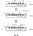
- FIGS. 3A-3B conceptually illustrate a side view sequence of how a package substrate that includes fine pitch traces can be manufactured in order to reduce misalignment during testing of the package substrate.
- FIGS. 3A-3B illustrate a side view sequence for manufacturing a package substrate that includes testing pads on fine pitch traces.
- the package substrate of FIGS. 3A-3B is a package substrate on which a fine pitch flip chip is mounted on during an assembly process.
- a fine pitch flip chip may be a flip chip that has an input / output (I/O) connection pitch of 100 microns ( ⁇ m) or less.
- an I/O connection pitch of a flip chip / die is a center to center distance between two neighboring I/O connections (e.g., under bump metallization (UBM) structures, bumps).
- these I/O connections are interconnects that are coupled to traces (e.g., fine pitch traces) on a package substrate.
- traces e.g., fine pitch traces
- Examples of a fine pitch flip chip may include a thermo-compression / thermal compression flip chip / die and mass reflow flip chip / die in some implementations.
- a package substrate 300 includes several traces (e.g., traces 302-304) and at least one pad (e.g., via pad 306) at the end of at least some of the traces.
- the traces are fine pitch traces that have a pitch of 100 microns ( ⁇ m) or less. In some implementations, a pitch defines a center to center distance between two neighboring traces.
- the package substrate 300 is at least partially covered with a solder resist layer 308.
- the pads e.g., via pad 306
- some portions of the traces are covered with the solder resist layer 308, leaving other portions of the traces exposed (e.g., leaving other portions of the traces free of the solder resist layer 308).
- stage 2 of FIG. 3A illustrates traces (e.g., trace 302) that include a covered portion (e.g., covered with the solder resist layer 308) and an exposed portion (e.g., free of the solder resist layer 308).
- the exposed portion of the trace is the portion of the trace that a die (e.g., thermal compression flip chip) is coupled to during an assembly process of a die to the package substrate 300.
- the exposed portion of the trace is the portion of the trace that a bonding component (e.g., solder ball) of the die is coupled to during an assembly process of a die to the package substrate 300 (e.g., when a die is mounted on the package substrate).
- a bonding component e.g., solder ball
- the package substrate 300 includes testing pads that a pin of a testing device may couple to during testing of the package substrate 300.
- some or all of the pads e.g., via pad 306 are now at least partially exposed and no longer covered with the solder resist layer 308 (at least partially free of the solder resist layer 308).
- the pads may function as testing pads configured to couple to testing pins of a testing device during the testing of the package substrate.
- Different implementations may remove the solder resist layer 308 above the pads (e.g., via pad 306) differently.
- an etching process may be used (e.g., using laser etching) to selectively remove portions of the solder resist layer 308.
- Some traces may initially not have any via pads.
- trace 304 does not include any via pads.
- a pad e.g. testing pad
- a pad may be added to a trace after a solder resist layer has been provided (e.g., deposited) on the package substrate 300.
- a solder resist layer has been provided (e.g., deposited) on the package substrate 300.
- an opening 309 in the solder resist layer 308 has been created above a portion of the trace 304.
- the opening 309 is created by removing (e.g., etching) a portion of the solder resist layer 308.
- a testing pad 310 has been added to the package substrate 300 after the solder resist layer 308 has been provided.
- the testing pad 310 is created by a metal layer / component (e.g., copper) that is deposited / added to the portion of the package substrate 300 and trace 304 that is left exposed as a result of the removing (e.g., etching) of the solder resist layer 308.
- the testing pad 310 is at least partially exposed and is not covered by the solder resist layer 308 (at least partially free of the solder resist layer 308).
- the testing pad 310 is configured to couple to a pin of a testing device during testing of the substrate. Different implementations may add / create / manufacture the testing pads differently.
- FIGS. 3A-3B conceptually illustrate a side view of how a package substrate that includes fine pitch traces can be manufactured in order to reduce misalignment during testing of the package substrate.
- the sequence and process is not limited to a package substrate. Consequently, the sequence and process can be applied to other substrates as well.
- a sequence and process for manufacturing a similar package substrate that includes fine pitch traces will now be described from top and side view perspectives to better illustrate exposed and covered portions of a package substrate.
- FIGS. 4A-4D conceptually illustrate a top view and a side view sequence of how a package substrate that includes fine pitch traces can be manufactured in order to reduce misalignment during testing of the package substrate.
- FIGS. 4A-4D illustrate a top view and a side view sequence for manufacturing a package substrate that includes testing pads on fine pitch traces.
- FIGS. 4A-4D is similar to FIGS. 3A-3B , except that it also includes a top view perspective.
- the side view of FIGS. 4A-4D is a cross section of the top view from the perspective of the A-A plane of the top view of FIGS. 4A-4D .
- a package substrate 400 includes several traces (e.g., traces 402-404) and at least one pad (e.g., via pad 406) at the end of at least some of the traces.
- the traces are fine pitch traces that have a pitch of 100 microns ( ⁇ m) or less. In some implementations, a pitch defines a center to center distance between two neighboring traces.
- the package substrate 300 is at least partially covered with a solder resist layer 308.
- the pads e.g., via pad 306 and some portions of the traces are covered with the solder resist layer 308, leaving other portions of the traces exposed (e.g., leaving other portions of the traces free of the solder resist layer 308).
- stage 2 of FIG. 4B illustrates traces (e.g., trace 302) that include a covered portion (e.g., covered with the solder resist layer 308) and an exposed portion (e.g., free of the solder resist layer 308).
- the exposed portion of the trace is the portion of the trace that a die (e.g., thermal compression flip chip) is coupled to during an assembly process of a die to the package substrate 300.
- the exposed portion of the trace is the portion of the trace that a bonding component (e.g., solder ball) of the die is coupled to during an assembly process of a die to the package substrate 300 (e.g., when a die is mounted on the package substrate).
- a bonding component e.g., solder ball
- the package substrate 300 includes testing pads that a pin of a testing device may couple to during testing of the package substrate 300.
- some or all of the pads e.g., via pad 306 are now at least partially exposed and no longer covered with the solder resist layer 308 (at least partially free of the solder resist layer 308).
- the pads may function as testing pads configured to couple to testing pins of a testing device during the testing of the package substrate.
- Different implementations may remove the solder resist layer 308 above the pads (e.g., via pad 306) differently.
- an etching process may be used (e.g., using laser etching) to selectively remove portions of the solder resist layer 308.
- Some traces may initially not have any via pads.
- trace 304 does not include any via pads.
- a pad e.g. testing pad
- a pad may be added to a trace after a solder resist layer has been provided (e.g., deposited) on the package substrate 300.
- a solder resist layer has been provided (e.g., deposited) on the package substrate 300.
- an opening 309 in the solder resist layer 308 has been created above a portion of the trace 304.
- the opening 309 is created by removing (e.g., etching) a portion of the solder resist layer 308.
- a testing pad 310 has been added to the package substrate 300 after the solder resist layer 308 has been provided.
- the testing pad 310 is created by a metal layer / component (e.g., copper) that is deposited / added to the portion of the package substrate 300 and trace 304 that is left exposed as a result of the removing (e.g., etching) of the solder resist layer 308.
- the testing pad 310 is at least partially exposed and is not covered by the solder resist layer 308 (at least partially free of the solder resist layer 308).
- the testing pad 310 is configured to couple to a pin of a testing device during testing of the substrate. Different implementations may add / create / manufacture the testing pads differently.
- the sequence of FIGS. 4A-4D illustrates an example of a sequence for manufacturing testing pads on a package substrate.
- the package substrate of FIGS. 4A-4D is a package substrate on which a fine pitch flip chip is mounted on during an assembly process.
- a fine pitch flip chip may be a flip chip / die that has an input / output (I/O) connection pitch of 100 microns ( ⁇ m) or less.
- an I/O connection pitch of a flip chip / die is a center to center distance between two neighboring I/O connections (e.g., under bump metallization (UBM) structures, bumps).
- UBM under bump metallization
- these I/O connections are interconnects that are coupled to traces (e.g., fine pitch traces) on a package substrate.
- traces e.g., fine pitch traces
- Examples of a fine pitch flip chip may include a thermo-compression / thermal compression flip chip / die and mass reflow flip chip / die in some implementations.
- FIGS. 4A-4D conceptually illustrates top and side views of how a package substrate that includes fine pitch traces can be manufactured in order to reduce misalignment during testing of the package substrate.
- the sequence and process is not limited to a package substrate. Consequently, the sequence and process can be applied to other substrates as well.
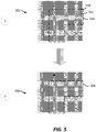
- FIG. 5 conceptually illustrates a more detailed top view of how a package substrate that includes fine pitch traces can be manufactured in order to reduce misalignment during testing of the package substrate.
- a package substrate 500 includes several traces (e.g., trace 502) and several pads. These traces are fine pitch traces having a pitch of 100 microns ( ⁇ m) or less. The pads may be via pads in some implementations.
- FIG. 5 also illustrates that a solder resist layer 504 covering some portions of some of the traces, leaving other portions of the traces exposed (e.g., leaving other portions of the traces free of the solder resist layer 504).
- a region 506 of the package substrate is exposed and free of the solder resist layer 504.
- the exposed region 506 is the region of the package substrate 500 that a die / chip (e.g., thermal compression flip chip) is coupled to during an assembly process of a die / chip to a package substrate.
- a die / chip e.g., thermal compression flip chip
- Stage 2 of FIG. 5 illustrates the package substrate 500 that includes testing pads that a testing pin of a testing device may couple to during testing of the package substrate.
- some or all of the pads (e.g., via pads) in region 508 of the package substrate 500 are now at least partially exposed and no longer covered with the solder resist layer 504 (at least partially free of the solder resist layer).
- one or more of these exposed pads are testing pads on which pins of a testing device may be coupled to during a test of the package substrate.
- Different implementations may remove the solder resist layer 504 above the pads (e.g., via pads) differently.
- an etching process may be used (e.g., using laser etching) to selectively remove portions of the solder resist layer 504.
- the sequence of FIG. 5 illustrates an example of a shortened sequence for manufacturing testing pads on a package substrate.
- the package substrate of FIG. 5 is a package substrate on which a fine pitch flip chip is mounted on during an assembly process.
- a fine pitch flip chip may be a flip chip / die that has an input / output (I/O) connection pitch of 100 microns ( ⁇ m) or less.
- I/O connection pitch of a flip chip / die is a center to center distance between two neighboring I/O connections (e.g., under bump metallization (UBM) structures, bumps).
- UBM under bump metallization
- these I/O connections are interconnects that are coupled to traces (e.g., fine pitch traces) on a package substrate.
- traces e.g., fine pitch traces
- Examples of a fine pitch flip chip may include a thermo-compression / thermal compression flip chip / die and mass reflow flip chip / die in some implementations.
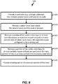
- FIG. 6 illustrates a flow diagram for providing / manufacturing a package substrate that includes testing pads on fine pitch traces.
- the method provides (at 605) a substrate (e.g., package substrate) that includes several traces and several pads (e.g., via pads).
- the substrate is a package substrate on which a thermal compression flip chip is mounted during an assembly process.
- FIGS. 2A and 4A illustrate examples of providing a substrate that includes several traces and several pads (e.g., via pads).
- the traces are fine pitch traces that have a pitch of 100 microns ( ⁇ m) or less.
- a trace pitch defines a center to center distance between two neighboring traces.
- the method provides (at 610) a solder resist layer above the several traces and the several pads of the substrate.
- a solder resist layer above the several traces and the several pads of the substrate.
- the substrate e.g., package substrate
- the solder resist layer only a portion of the substrate (e.g., package substrate) is covered by the solder resist layer. Consequently, in some implementations, only a portion of the traces on the substrate may be covered by the solder resist layer.
- Stage 2 of FIG. 2B and FIG. 4B illustrate examples of providing a solder resist layer above several traces and several pads (e.g., via pads).
- the method removes (at 615) a portion of the solder resist layer to at least partially expose at least one pad (e.g., via pad).
- a pad e.g., via pad
- Different implementations may remove the solder resist layer to expose a pad differently.
- an etching process may be used (e.g., using laser etching) to selectively remove portions of the solder resist layer.
- removing a portion of the solder resist layer creates an opening in the solder resist layer above the pad (e.g., via pad)
- the exposed pad is at least partially free of the solder resist layer.
- the exposed pad (e.g., exposed via pad) is configured to be a testing pad configured to couple to a pin of a testing device during testing of the substrate.
- the testing pad is free of a direct connection with a bonding component of a die (e.g., flip chip) when the die is coupled to the substrate.
- Stage 3 of FIG. 2B and FIG. 4C illustrate examples of removing a portion of a solder resist layer to expose a pad (e.g., via pad).
- the method removes (at 620) a portion of the solder resist layer to at least partially expose one portion of a trace.
- Different implementations may remove the solder resist layer to expose a portion of a trace differently.
- an etching process may be used (e.g., using laser etching) to selectively remove portions of the solder resist layer.
- removing a portion of the solder resist layer creates an opening in the solder resist layer above a portion of the trace. The exposed portion of the trace is at least partially free of the solder resist layer.
- removing (at 620) the portion of the solder resist layer to at least partially expose a portion of a trace is performed before or concurrently with removing (at 615) the portion of the solder resist layer to at least partially expose one or more pads (e.g., via pads).
- FIG. 4C illustrate an example of removing a portion of a solder resist layer to expose a portion of a trace.
- the method provides (at 625) a testing pad on the at least partially exposed portion of the trace.
- the testing pad is provided (e.g., created) by a metal layer / component (e.g., copper) that is deposited / added to the portion of the package substrate and trace that is left exposed as a result of the removing (e.g., etching) of the solder resist layer (e.g., in the opening of the solder resist layer).
- the testing pad is at least partially exposed and is not covered by the solder resist layer (at least partially free of the solder resist layer.
- the testing pad is configured to couple to a pin of a testing device during testing of the substrate.
- the testing pad is free of a direct connection with a bonding component of a die (e.g., flip chip) when the die is coupled to the substrate.
- Stage 3 of FIG. 2B and FIG. 4D illustrate examples of providing testing pads on package substrate.
- the method of FIG. 6 illustrates an example of a method for manufacturing a package substrate with testing pads.
- the package substrate is a package substrate on which a fine pitch flip chip is mounted on during an assembly process.
- a fine pitch flip chip may be a flip chip / die that has an input / output (I/O) connection pitch of 100 microns ( ⁇ m) or less.
- an I/O connection pitch of a flip chip / die is a center to center distance between two neighboring I/O connections (e.g., under bump metallization (UBM) structures, bumps).
- these I/O connections are interconnects that are coupled to traces (e.g., fine pitch traces) on a package substrate.
- Examples of a fine pitch flip chip may include a thermo-compression / thermal compression flip chip / die and mass reflow flip chip / die in some implementations.
- FIG. 7 illustrates various electronic devices that may be integrated with any of the aforementioned integrated circuit, die, chip or package.
- a mobile telephone 702, a laptop computer 704, and a fixed location terminal 706 may include an integrated circuit (IC) 700 as described herein.
- the IC 700 may be, for example, any of the integrated circuits, dice or packages described herein.
- the devices 702, 704, 706 illustrated in FIG. 7 are merely exemplary.
- IC 700 may also feature the IC 700 including, but not limited to, mobile devices, hand-held personal communication systems (PCS) units, portable data units such as personal digital assistants, GPS enabled devices, navigation devices, set top boxes, music players, video players, entertainment units, fixed location data units such as meter reading equipment, communications devices, smartphones, tablet computers or any other device that stores or retrieves data or computer instructions, or any combination thereof.
- PCS personal communication systems
- FIGS. 2A-2B , 3A-3B , 4A-4D , 5 , 6 and/or 7 may be rearranged and/or combined into a single component, step, feature or function or embodied in several components, steps, or functions.
- FIGs One or more of the components, steps, features and/or functions illustrated in the FIGs may be rearranged and/or combined into a single component, step, feature or function or embodied in several components, steps, or functions. Additional elements, components, steps, and/or functions may also be added without departing from novel features disclosed herein.
- the apparatus, devices, and/or components illustrated in the FIGs may be configured to perform one or more of the methods, features, or steps described in the FIGs.
- the novel algorithms described herein may also be efficiently implemented in software and/or embedded in hardware.
- the word "exemplary” is used herein to mean “serving as an example, instance, or illustration.” Any implementation or aspect described herein as “exemplary” is not necessarily to be construed as preferred or advantageous over other aspects of the disclosure. Likewise, the term “aspects” does not require that all aspects of the disclosure include the discussed feature, advantage or mode of operation.
- the term “coupled” is used herein to refer to the direct or indirect coupling between two objects. For example, if object A physically touches object B, and object B touches object C, then objects A and C may still be considered coupled to one another-even if they do not directly physically touch each other.
- die package is used to refer to an integrated circuit wafer that has been encapsulated or packaged or encapsulated.
- the embodiments may be described as a process that is depicted as a flowchart, a flow diagram, a structure diagram, or a block diagram. Although a flowchart may describe the operations as a sequential process, many of the operations can be performed in parallel or concurrently. In addition, the order of the operations may be re-arranged.
- a process is terminated when its operations are completed.
- a process may correspond to a method, a function, a procedure, a subroutine, a subprogram, etc.
- a process corresponds to a function
- its termination corresponds to a return of the function to the calling function or the main function.
Description
- Various features relate to a package substrate with testing pads on fine pitch traces.
- A thermal compression bonding process is a process used to assemble / package a flip chip, die or semiconductor device to a package substrate. Such a flip chip is often referred to as a thermal compression flip chip (TCFC). Thermal compression bonding processes provide several advantages over traditional bonding processes. For example, thermal compression bonding processes are generally more accurate than other solder bonding processes. Thus, thermal compression bonding processes are ideal when using fine pitch traces on a substrate (e.g., less than 100 microns (µm)). In contrast, other solder bonding processes are limited to a bonding pitch that is greater than 100 microns (µm). Thus, TCFCs are typically higher density chips than chips using other bonding processes.
- However, testing package substrates having fine pitch traces (e.g., 100 microns (µm) or less) can be challenging and difficult due to the small size of the pitches of the traces. Specifically, fine pitch traces may result in misalignment when pins of a testing device are connected to the traces on the substrate.
FIG. 1 illustrates such an example. Specifically,FIG. 1 conceptually illustrates apackage substrate 100 that includes severalfine pitch traces 102.FIG. 1 also illustratesseveral testing pins 104 being electrically coupled to thetraces 102. As shown inFIG. 1 , thetesting pins 104 are not aligned with thetraces 102. The result of this misalignment is that the package substrate may not be properly tested. - Therefore, there is a need for an improved method for testing package substrates with fine pitch traces. Ideally, such a solution will be cost effective and reduce testing errors due to misalignment of testing pins of a testing device.
- In
US 2010/0012356 A1 of Hasegawa , there is disclosed a printed wiring board comprising an insulating substrate having a mounting surface, a recognition mark formed on the mounting surface of the insulating substrate, and a plurality of reinforcing patterns formed on the mounting surface of the insulating substrate. The reinforcing patterns extend from an outer periphery of the recognition mark toward outside of the recognition mark and are arranged circumferentially at intervals relative to the recognition mark. Each of the reinforcing patterns has a width less than a width of a part of the outer periphery of the recognition mark connecting adjacent ones of the reinforcing patterns. - In
US 2008/0048695 A1 of Ashida there is disclosed a circuit substrate provided with a plurality of circuit blocks formed on a single substrate, at least one of the metal patterns connecting the circuit blocks being separated into two sections at some midpoint of wiring, and exposed conductor portions whose end portions are to be bridge-connected through soldering are provided at the end portions in the separated portion of the separated two wiring metal patterns. - Various features relate to a package substrate with testing pads on fine pitch traces. A substrate according to the invention is defined in
independent claim 1 and a corresponding method according to the invention is defined in independent claim 12. - A first example provides a substrate for receiving a chip, comprising: a plurality of traces; a solder resist layer covering the plurality of traces; an exposed portion for receiving the chip, the exposed portion being free of the solder resist layer and exposing portions of the plurality of traces for electrical connection with the chip; and a testing pad coupled to a trace from the plurality of traces, the testing pad being at least partially exposed and at least partially free of the solder resist layer and positioned at a location other than an end of the trace..
- According to an aspect, the several traces have a pitch that is 100 microns (µm) or less. In some implementations, the substrate is a package substrate. In some implementations, the package substrate is a package substrate on which a fine pitch flip chip is mounted during an assembly process. In some implementations, the fine pitch flip chip is a thermo-compression flip chip. In some implementations, the fine pitch flip chip is a mass reflow flip chip.
- According to one aspect, the testing pad is free of a direct connection with a bonding component of the chip when the chip is coupled to the substrate. In some implementations, the bonding component is one of a solder ball. In some implementations, the bonding component is one of a solder ball.
- According to an aspect, the testing pad is a via pad that traverses at least part of the substrate.
- According to one aspect, the testing pad has a width that is larger than the width of the trace to which the testing pad is coupled to.
- According to an aspect, the testing pad is configured to couple to a pin of a testing device during testing of the substrate.
- According to one aspect, the substrate is incorporated into at least one of a music player, a video player, an entertainment unit, a navigation device, a communications device, a mobile device, a mobile phone, a smartphone, a personal digital assistant, a fixed location terminal, a tablet computer, and/or a laptop computer.
- A third example provides a method for providing a substrate. The method comprises: providing a substrate that includes a plurality of traces; providing a solder resist layer covering the plurality of traces; providing an exposed portion for receiving a chip, the exposed portion being free of the solder resist layer and exposing portions of the plurality of traces for electrical connection with the chip; removing a portion of the solder resist layer to at least partially expose at least one testing pad, the testing pad being at least partially exposed and at least partially free of the solder resist layer; removing a portion of the solder resist layer to at least partially expose at least one portion of a trace at a location other than an end of the trace, the portion of the trace being at least partially free of solder resist layer; and providing an additional testing pad on the exposed portion of the trace..
- According to an aspect, the method further couples the substrate to the chip such that the testing pad remains at least partially exposed and at least partially free of the solder resist layer.
- According to an aspect, the several traces have a pitch that is 100 microns (µm) or less. In some implementations, the substrate is a package substrate. In some implementations, the package substrate is a package substrate on which a fine pitch flip chip is mounted during an assembly process. In some implementations, the fine pitch flip chip is a thermo-compression flip chip. In some implementations, the fine pitch flip chip is a mass reflow flip chip.
- According to one aspect, the testing pad is free of a direct connection with a bonding component of the chip when the chip is coupled to the substrate. In some implementations, the bonding component is one of a solder ball. In some implementations, the bonding component is one of a solder ball.
- According to an aspect, the testing pad is a via pad that traverses at least part of the substrate.
- According to one aspect, the testing pad has a width that is larger than the width of the trace to which the testing pad is coupled to.
- According to an aspect, the testing pad is configured to couple to a pin of a testing device during testing of the substrate.
- According to one aspect, the method further incorporates the substrate into at least one of a music player, a video player, an entertainment unit, a navigation device, a communications device, a mobile device, a mobile phone, a smartphone, a personal digital assistant, a fixed location terminal, a tablet computer, and/or a laptop computer.
- Various features, nature and advantages may become apparent from the detailed description set forth below when taken in conjunction with the drawings in which like reference characters identify correspondingly throughout.
-
FIG. 1 illustrates a package substrate that includes several fine pitch traces. -
FIGS. 2A-2B illustrate a top view sequence for manufacturing a package substrate that includes testing pads on fine pitch traces. -
FIGS. 3A-3B illustrate a side view sequence for manufacturing a package substrate that includes testing pads on fine pitch traces. -
FIGS. 4A-4D illustrate another sequence for manufacturing a package substrate that includes testing pads on fine pitch traces. -
FIG. 5 illustrates a detailed view of a sequence for manufacturing a package substrate that includes testing pads on fine pitch traces. -
FIG. 6 illustrates a flow diagram for manufacturing a package substrate that includes testing pads on fine pitch traces. -
FIG. 7 illustrates various electronic devices that may be integrated with any of the aforementioned integrated circuit, die, chip, die package and/or substrate. - In the following description, specific details are given to provide a thorough understanding of the various aspects of the disclosure. However, it will be understood by one of ordinary skill in the art that the aspects may be practiced without these specific details. For example, circuits may be shown in block diagrams in order to avoid obscuring the aspects in unnecessary detail. In other instances, well-known circuits, structures and techniques may not be shown in detail in order not to obscure the aspects of the disclosure.
- Some novel features pertain to a substrate that includes several traces, a solder resist layer covering the several traces, and a testing pad coupled to a trace from the several traces. The testing pad is at least partially exposed and at least partially free of the solder resist layer when a chip is coupled to the substrate. In some implementations, the several traces have a pitch that is 100 microns (µm) or less. In some implementations, traces that have a pitch of 100 microns (µm) or less may be referred as fine pitch traces. In some implementations, the substrate is a package substrate. In some implementations, the package substrate is a package substrate on which a thermal compression flip chip is mounted during an assembly process. In some implementations, the package substrate is a package substrate on which a mass reflow flip chip is mounted during an assembly process. In some implementations, the testing pad is free of a direct connection with a bonding component of the chip when the chip is coupled to the substrate. In some implementations, the bonding component is one of a solder ball.
-
FIGS. 2A-2B conceptually illustrate a top view sequence of how a package substrate that includes fine pitch traces can be manufactured in order to reduce misalignment during testing of the package substrate. Specifically,FIGS. 2A-2B illustrate a top view sequence for manufacturing a package substrate that includes testing pads on fine pitch traces. In some implementations, fine pitch traces are traces that have a pitch of 100 microns (µm) or less. A pitch of a trace may be a center to center distance between tow neighboring traces. In some implementations, the package substrate is a package substrate on which a fine pitch flip chip is mounted on during an assembly process. In some implementations, a fine pitch flip chip may be a flip chip / die that has an input / output (I/O) connection pitch of 100 microns (µm) or less. In some implementations, an I/O connection pitch of a flip chip is a center to center distance between two neighboring I/O connections (e.g., under bump metallization (UBM) structures, bumps). In some implementations, these I/O connections are interconnects that are coupled to traces (e.g., fine pitch traces) on a package substrate. Examples of a fine pitch flip chip may include a thermo-compression / thermal compression flip chip / die and mass reflow flip chip / die in some implementations. - As shown in
FIG. 2A , atstage 1, apackage substrate 200 includes several traces (e.g., traces 202-204) and several pads (e.g., via pad 206) at the end of at least some of the traces. The traces are fine pitch traces that have a pitch of 100 microns (µm) or less. In some implementations, a trace pitch defines a center to center distance between two neighboring traces. - As further shown in
FIG. 2B , atstage 2, thepackage substrate 200 is at least partially covered with a solder resistlayer 208. Atstage 2, the pads (e.g., via pad 206) and some portions of the traces are covered with the solder resistlayer 208, leaving other portions of the traces exposed (e.g., leaving other portions of the traces free of the solder resist layer 208). Thus,stage 2 ofFIG. 2B illustrates traces (e.g., trace 202) that include a covered portion (e.g., covered with the solder resist layer 208) and an exposed portion (e.g., free of the solder resist layer 208). In some implementations, the exposed portion of the trace is the portion of the trace that a die (e.g., thermal compression flip chip) is coupled to during an assembly process of a die to thepackage substrate 200. For example, in some implementations, the exposed portion of the trace is the portion of the trace that a bonding component (e.g., solder ball) of the die is coupled to during an assembly process of a die to the package substrate 200 (e.g., when a die is mounted on the package substrate). - At
stage 3 ofFIG. 2B , thepackage substrate 200 includes testing pads that a pin of a testing device may couple to during testing of thepackage substrate 200. As shown instage 3, some or all of the pads (e.g., via pad 206) are now at least partially exposed and no longer covered with the solder resist layer 208 (at least partially free of the solder resist layer 208). Once the solder resistlayer 208 above the pads has been removed (e.g., etched), the pads may function as testing pads configured to couple to testing pins of a testing device during the testing of the package substrate. Different implementations may remove the solder resistlayer 208 above the pads (e.g., via pad 206) differently. In some implementations, an etching process may be used (e.g., using laser etching) to selectively remove portions of the solder resistlayer 208. - Some traces (e.g., trace 202) may initially not have any via pads. For example, trace 202 at
stage 1 does not include any via pads. In some implementations, a pad (e.g. testing pad) may be added to a trace after a solder resist layer has been provided (e.g., deposited) on thepackage substrate 200. As shown atstage 3 ofFIG. 2B , several testing pads (e.g., testing pads 210-214) have been added to thepackage substrate 200 after the solder resistlayer 208 has been provided. The testing pads 210-214 are at least partially exposed and are not covered by the solder resist layer 208 (at least partially free of the solder resist layer 208). In some implementations, the testing pads 210-214 are configured to couple to a pin of a testing device during testing of the substrate. - Different implementations may add / create / manufacture the testing pads differently. In some implementations, a portion of the solder resist
layer 208 above a portion of a trace (e.g., trace 202) is etched away, leaving an opening in the solder resistlayer 208 and exposing a portion of the trace (e.g., portion of trace 202). A metal layer / component (e.g., copper) is then deposited / added to the portion of the package substrate and trace that is left exposed as a result of the removing (e.g., etching) of the solder resistlayer 208. -
FIGS. 2A-2B conceptually illustrate a top view of how a package substrate that includes fine pitch traces can be manufactured in order to reduce misalignment during testing of the package substrate. However, the sequence and process is not limited to a package substrate. Consequently, the sequence and process can be applied to other substrates as well. A sequence and process for manufacturing a similar package substrate that includes fine pitch traces will now be described from a side view perspective. -
FIGS. 3A-3B conceptually illustrate a side view sequence of how a package substrate that includes fine pitch traces can be manufactured in order to reduce misalignment during testing of the package substrate. Specifically,FIGS. 3A-3B illustrate a side view sequence for manufacturing a package substrate that includes testing pads on fine pitch traces. In some implementations, the package substrate ofFIGS. 3A-3B is a package substrate on which a fine pitch flip chip is mounted on during an assembly process. In some implementations, a fine pitch flip chip may be a flip chip that has an input / output (I/O) connection pitch of 100 microns (µm) or less. In some implementations, an I/O connection pitch of a flip chip / die is a center to center distance between two neighboring I/O connections (e.g., under bump metallization (UBM) structures, bumps). In some implementations, these I/O connections are interconnects that are coupled to traces (e.g., fine pitch traces) on a package substrate. Examples of a fine pitch flip chip may include a thermo-compression / thermal compression flip chip / die and mass reflow flip chip / die in some implementations. - As shown in
FIG. 3A , atstage 1, apackage substrate 300 includes several traces (e.g., traces 302-304) and at least one pad (e.g., via pad 306) at the end of at least some of the traces. The traces are fine pitch traces that have a pitch of 100 microns (µm) or less. In some implementations, a pitch defines a center to center distance between two neighboring traces. - As shown at
stage 2, thepackage substrate 300 is at least partially covered with a solder resistlayer 308. Although not visible from a side view, atstage 2, the pads (e.g., via pad 306) and some portions of the traces are covered with the solder resistlayer 308, leaving other portions of the traces exposed (e.g., leaving other portions of the traces free of the solder resist layer 308). Thus,stage 2 ofFIG. 3A illustrates traces (e.g., trace 302) that include a covered portion (e.g., covered with the solder resist layer 308) and an exposed portion (e.g., free of the solder resist layer 308). In some implementations, the exposed portion of the trace is the portion of the trace that a die (e.g., thermal compression flip chip) is coupled to during an assembly process of a die to thepackage substrate 300. For example, in some implementations, the exposed portion of the trace is the portion of the trace that a bonding component (e.g., solder ball) of the die is coupled to during an assembly process of a die to the package substrate 300 (e.g., when a die is mounted on the package substrate). - At
stage 3 ofFIG. 3A , thepackage substrate 300 includes testing pads that a pin of a testing device may couple to during testing of thepackage substrate 300. As shown instage 3, some or all of the pads (e.g., via pad 306) are now at least partially exposed and no longer covered with the solder resist layer 308 (at least partially free of the solder resist layer 308). Once the solder resistlayer 308 above the pads has been removed (e.g., etched), the pads may function as testing pads configured to couple to testing pins of a testing device during the testing of the package substrate. Different implementations may remove the solder resistlayer 308 above the pads (e.g., via pad 306) differently. In some implementations, an etching process may be used (e.g., using laser etching) to selectively remove portions of the solder resistlayer 308. - Some traces (e.g., trace 304) may initially not have any via pads. For example,
trace 304 does not include any via pads. In some implementations, a pad (e.g. testing pad) may be added to a trace after a solder resist layer has been provided (e.g., deposited) on thepackage substrate 300. As shown atstage 3, anopening 309 in the solder resistlayer 308 has been created above a portion of thetrace 304. In some implementations, theopening 309 is created by removing (e.g., etching) a portion of the solder resistlayer 308. - As shown at
stage 4 ofFIG. 3B , atesting pad 310 has been added to thepackage substrate 300 after the solder resistlayer 308 has been provided. In some implementations, thetesting pad 310 is created by a metal layer / component (e.g., copper) that is deposited / added to the portion of thepackage substrate 300 and trace 304 that is left exposed as a result of the removing (e.g., etching) of the solder resistlayer 308. Thetesting pad 310 is at least partially exposed and is not covered by the solder resist layer 308 (at least partially free of the solder resist layer 308). In some implementations, thetesting pad 310 is configured to couple to a pin of a testing device during testing of the substrate. Different implementations may add / create / manufacture the testing pads differently. -
FIGS. 3A-3B conceptually illustrate a side view of how a package substrate that includes fine pitch traces can be manufactured in order to reduce misalignment during testing of the package substrate. However, the sequence and process is not limited to a package substrate. Consequently, the sequence and process can be applied to other substrates as well. - A sequence and process for manufacturing a similar package substrate that includes fine pitch traces will now be described from top and side view perspectives to better illustrate exposed and covered portions of a package substrate.
-
FIGS. 4A-4D conceptually illustrate a top view and a side view sequence of how a package substrate that includes fine pitch traces can be manufactured in order to reduce misalignment during testing of the package substrate. Specifically,FIGS. 4A-4D illustrate a top view and a side view sequence for manufacturing a package substrate that includes testing pads on fine pitch traces.FIGS. 4A-4D is similar toFIGS. 3A-3B , except that it also includes a top view perspective. It should be noted that the side view ofFIGS. 4A-4D is a cross section of the top view from the perspective of the A-A plane of the top view ofFIGS. 4A-4D . - As shown in
FIG. 4A , atstage 1, a package substrate 400 includes several traces (e.g., traces 402-404) and at least one pad (e.g., via pad 406) at the end of at least some of the traces. The traces are fine pitch traces that have a pitch of 100 microns (µm) or less. In some implementations, a pitch defines a center to center distance between two neighboring traces. - As shown in
FIG. 4B , atstage 2, thepackage substrate 300 is at least partially covered with a solder resistlayer 308. Atstage 2, the pads (e.g., via pad 306) and some portions of the traces are covered with the solder resistlayer 308, leaving other portions of the traces exposed (e.g., leaving other portions of the traces free of the solder resist layer 308). Thus,stage 2 ofFIG. 4B illustrates traces (e.g., trace 302) that include a covered portion (e.g., covered with the solder resist layer 308) and an exposed portion (e.g., free of the solder resist layer 308). In some implementations, the exposed portion of the trace is the portion of the trace that a die (e.g., thermal compression flip chip) is coupled to during an assembly process of a die to thepackage substrate 300. For example, in some implementations, the exposed portion of the trace is the portion of the trace that a bonding component (e.g., solder ball) of the die is coupled to during an assembly process of a die to the package substrate 300 (e.g., when a die is mounted on the package substrate). - As shown at
stage 3 ofFIG. 4C , thepackage substrate 300 includes testing pads that a pin of a testing device may couple to during testing of thepackage substrate 300. As shown instage 3, some or all of the pads (e.g., via pad 306) are now at least partially exposed and no longer covered with the solder resist layer 308 (at least partially free of the solder resist layer 308). Once the solder resistlayer 308 above the pads has been removed (e.g., etched), the pads may function as testing pads configured to couple to testing pins of a testing device during the testing of the package substrate. Different implementations may remove the solder resistlayer 308 above the pads (e.g., via pad 306) differently. In some implementations, an etching process may be used (e.g., using laser etching) to selectively remove portions of the solder resistlayer 308. - Some traces (e.g., trace 304) may initially not have any via pads. For example,
trace 304 does not include any via pads. In some implementations, a pad (e.g. testing pad) may be added to a trace after a solder resist layer has been provided (e.g., deposited) on thepackage substrate 300. As shown atstage 3, anopening 309 in the solder resistlayer 308 has been created above a portion of thetrace 304. In some implementations, theopening 309 is created by removing (e.g., etching) a portion of the solder resistlayer 308. - As shown at
stage 4 ofFIG. 4D , atesting pad 310 has been added to thepackage substrate 300 after the solder resistlayer 308 has been provided. In some implementations, thetesting pad 310 is created by a metal layer / component (e.g., copper) that is deposited / added to the portion of thepackage substrate 300 and trace 304 that is left exposed as a result of the removing (e.g., etching) of the solder resistlayer 308. Thetesting pad 310 is at least partially exposed and is not covered by the solder resist layer 308 (at least partially free of the solder resist layer 308). In some implementations, thetesting pad 310 is configured to couple to a pin of a testing device during testing of the substrate. Different implementations may add / create / manufacture the testing pads differently. - The sequence of
FIGS. 4A-4D illustrates an example of a sequence for manufacturing testing pads on a package substrate. In some implementations, the package substrate ofFIGS. 4A-4D is a package substrate on which a fine pitch flip chip is mounted on during an assembly process. In some implementations, a fine pitch flip chip may be a flip chip / die that has an input / output (I/O) connection pitch of 100 microns (µm) or less. In some implementations, an I/O connection pitch of a flip chip / die is a center to center distance between two neighboring I/O connections (e.g., under bump metallization (UBM) structures, bumps). In some implementations, these I/O connections are interconnects that are coupled to traces (e.g., fine pitch traces) on a package substrate. Examples of a fine pitch flip chip may include a thermo-compression / thermal compression flip chip / die and mass reflow flip chip / die in some implementations. -
FIGS. 4A-4D conceptually illustrates top and side views of how a package substrate that includes fine pitch traces can be manufactured in order to reduce misalignment during testing of the package substrate. However, the sequence and process is not limited to a package substrate. Consequently, the sequence and process can be applied to other substrates as well. -
FIG. 5 conceptually illustrates a more detailed top view of how a package substrate that includes fine pitch traces can be manufactured in order to reduce misalignment during testing of the package substrate. As shown inFIG. 5 , duringstage 1, apackage substrate 500 includes several traces (e.g., trace 502) and several pads. These traces are fine pitch traces having a pitch of 100 microns (µm) or less. The pads may be via pads in some implementations.FIG. 5 also illustrates that a solder resistlayer 504 covering some portions of some of the traces, leaving other portions of the traces exposed (e.g., leaving other portions of the traces free of the solder resist layer 504). For example, aregion 506 of the package substrate is exposed and free of the solder resistlayer 504. In some implementations, the exposedregion 506 is the region of thepackage substrate 500 that a die / chip (e.g., thermal compression flip chip) is coupled to during an assembly process of a die / chip to a package substrate. -
Stage 2 ofFIG. 5 illustrates thepackage substrate 500 that includes testing pads that a testing pin of a testing device may couple to during testing of the package substrate. As shown instage 2, some or all of the pads (e.g., via pads) inregion 508 of thepackage substrate 500 are now at least partially exposed and no longer covered with the solder resist layer 504 (at least partially free of the solder resist layer). In some implementations, one or more of these exposed pads are testing pads on which pins of a testing device may be coupled to during a test of the package substrate. Different implementations may remove the solder resistlayer 504 above the pads (e.g., via pads) differently. In some implementations, an etching process may be used (e.g., using laser etching) to selectively remove portions of the solder resistlayer 504. - The sequence of
FIG. 5 illustrates an example of a shortened sequence for manufacturing testing pads on a package substrate. In some implementations, the package substrate ofFIG. 5 is a package substrate on which a fine pitch flip chip is mounted on during an assembly process. In some implementations, a fine pitch flip chip may be a flip chip / die that has an input / output (I/O) connection pitch of 100 microns (µm) or less. In some implementations, an I/O connection pitch of a flip chip / die is a center to center distance between two neighboring I/O connections (e.g., under bump metallization (UBM) structures, bumps). In some implementations, these I/O connections are interconnects that are coupled to traces (e.g., fine pitch traces) on a package substrate. Examples of a fine pitch flip chip may include a thermo-compression / thermal compression flip chip / die and mass reflow flip chip / die in some implementations. - Having described various examples of a package substrate that includes testing pads on fine pitch traces, a method for manufacturing a package substrate that includes testing pads on fine pitch traces will now be described below.
-
FIG. 6 illustrates a flow diagram for providing / manufacturing a package substrate that includes testing pads on fine pitch traces. The method provides (at 605) a substrate (e.g., package substrate) that includes several traces and several pads (e.g., via pads). In some implementations, the substrate is a package substrate on which a thermal compression flip chip is mounted during an assembly process.FIGS. 2A and4A illustrate examples of providing a substrate that includes several traces and several pads (e.g., via pads). In some implementations, the traces are fine pitch traces that have a pitch of 100 microns (µm) or less. In some implementations, a trace pitch defines a center to center distance between two neighboring traces. - The method provides (at 610) a solder resist layer above the several traces and the several pads of the substrate. In some implementations, only a portion of the substrate (e.g., package substrate) is covered by the solder resist layer. Consequently, in some implementations, only a portion of the traces on the substrate may be covered by the solder resist layer.
Stage 2 ofFIG. 2B andFIG. 4B illustrate examples of providing a solder resist layer above several traces and several pads (e.g., via pads). - The method removes (at 615) a portion of the solder resist layer to at least partially expose at least one pad (e.g., via pad). Different implementations may remove the solder resist layer to expose a pad differently. In some implementations, an etching process may be used (e.g., using laser etching) to selectively remove portions of the solder resist layer. In some implementations, removing a portion of the solder resist layer creates an opening in the solder resist layer above the pad (e.g., via pad) The exposed pad is at least partially free of the solder resist layer. The exposed pad (e.g., exposed via pad) is configured to be a testing pad configured to couple to a pin of a testing device during testing of the substrate. In some implementations, the testing pad is free of a direct connection with a bonding component of a die (e.g., flip chip) when the die is coupled to the substrate.
Stage 3 ofFIG. 2B andFIG. 4C illustrate examples of removing a portion of a solder resist layer to expose a pad (e.g., via pad). - The method removes (at 620) a portion of the solder resist layer to at least partially expose one portion of a trace. Different implementations may remove the solder resist layer to expose a portion of a trace differently. In some implementations, an etching process may be used (e.g., using laser etching) to selectively remove portions of the solder resist layer. In some implementations, removing a portion of the solder resist layer creates an opening in the solder resist layer above a portion of the trace. The exposed portion of the trace is at least partially free of the solder resist layer. In some implementations, removing (at 620) the portion of the solder resist layer to at least partially expose a portion of a trace is performed before or concurrently with removing (at 615) the portion of the solder resist layer to at least partially expose one or more pads (e.g., via pads).
FIG. 4C illustrate an example of removing a portion of a solder resist layer to expose a portion of a trace. - The method provides (at 625) a testing pad on the at least partially exposed portion of the trace. Different implementations may provide the testing pad differently. In some implementations, the testing pad is provided (e.g., created) by a metal layer / component (e.g., copper) that is deposited / added to the portion of the package substrate and trace that is left exposed as a result of the removing (e.g., etching) of the solder resist layer (e.g., in the opening of the solder resist layer). In some implementations, the testing pad is at least partially exposed and is not covered by the solder resist layer (at least partially free of the solder resist layer. In some implementations, the testing pad is configured to couple to a pin of a testing device during testing of the substrate. In some implementations, the testing pad is free of a direct connection with a bonding component of a die (e.g., flip chip) when the die is coupled to the substrate.
Stage 3 ofFIG. 2B andFIG. 4D illustrate examples of providing testing pads on package substrate. - The method of
FIG. 6 illustrates an example of a method for manufacturing a package substrate with testing pads. In some implementations, the package substrate is a package substrate on which a fine pitch flip chip is mounted on during an assembly process. In some implementations, a fine pitch flip chip may be a flip chip / die that has an input / output (I/O) connection pitch of 100 microns (µm) or less. In some implementations, an I/O connection pitch of a flip chip / die is a center to center distance between two neighboring I/O connections (e.g., under bump metallization (UBM) structures, bumps). In some implementations, these I/O connections are interconnects that are coupled to traces (e.g., fine pitch traces) on a package substrate. Examples of a fine pitch flip chip may include a thermo-compression / thermal compression flip chip / die and mass reflow flip chip / die in some implementations. -
FIG. 7 illustrates various electronic devices that may be integrated with any of the aforementioned integrated circuit, die, chip or package. For example, amobile telephone 702, alaptop computer 704, and a fixedlocation terminal 706 may include an integrated circuit (IC) 700 as described herein. TheIC 700 may be, for example, any of the integrated circuits, dice or packages described herein. Thedevices FIG. 7 are merely exemplary. Other electronic devices may also feature theIC 700 including, but not limited to, mobile devices, hand-held personal communication systems (PCS) units, portable data units such as personal digital assistants, GPS enabled devices, navigation devices, set top boxes, music players, video players, entertainment units, fixed location data units such as meter reading equipment, communications devices, smartphones, tablet computers or any other device that stores or retrieves data or computer instructions, or any combination thereof. - One or more of the components, steps, features, and/or functions illustrated in
FIGS. 2A-2B ,3A-3B ,4A-4D ,5 ,6 and/or7 may be rearranged and/or combined into a single component, step, feature or function or embodied in several components, steps, or functions. - One or more of the components, steps, features and/or functions illustrated in the FIGs may be rearranged and/or combined into a single component, step, feature or function or embodied in several components, steps, or functions. Additional elements, components, steps, and/or functions may also be added without departing from novel features disclosed herein. The apparatus, devices, and/or components illustrated in the FIGs may be configured to perform one or more of the methods, features, or steps described in the FIGs. The novel algorithms described herein may also be efficiently implemented in software and/or embedded in hardware.
- The word "exemplary" is used herein to mean "serving as an example, instance, or illustration." Any implementation or aspect described herein as "exemplary" is not necessarily to be construed as preferred or advantageous over other aspects of the disclosure. Likewise, the term "aspects" does not require that all aspects of the disclosure include the discussed feature, advantage or mode of operation. The term "coupled" is used herein to refer to the direct or indirect coupling between two objects. For example, if object A physically touches object B, and object B touches object C, then objects A and C may still be considered coupled to one another-even if they do not directly physically touch each other. The term "die package" is used to refer to an integrated circuit wafer that has been encapsulated or packaged or encapsulated.
- Also, it is noted that the embodiments may be described as a process that is depicted as a flowchart, a flow diagram, a structure diagram, or a block diagram. Although a flowchart may describe the operations as a sequential process, many of the operations can be performed in parallel or concurrently. In addition, the order of the operations may be re-arranged. A process is terminated when its operations are completed. A process may correspond to a method, a function, a procedure, a subroutine, a subprogram, etc. When a process corresponds to a function, its termination corresponds to a return of the function to the calling function or the main function.
- Those of skill in the art would further appreciate that the various illustrative logical blocks, modules, circuits, and algorithm steps described in connection with the embodiments disclosed herein may be implemented as electronic hardware, computer software, or combinations of both. To clearly illustrate this interchangeability of hardware and software, various illustrative components, blocks, modules, circuits, and steps have been described above generally in terms of their functionality. Whether such functionality is implemented as hardware or software depends upon the particular application and design constraints imposed on the overall system.
- The various features of the invention described herein can be implemented in different systems without departing from the invention. It should be noted that the foregoing aspects of the disclosure are merely examples and are not to be construed as limiting the invention. The description of the aspects of the present disclosure is intended to be illustrative, and not to limit the scope of the claims. As such, the present teachings can be readily applied to other types of apparatuses and many alternatives, modifications, and variations will be apparent to those skilled in the art, the scope of the invention being defined by the appended claims.
Claims (15)
- A substrate (200, 300, 500) for receiving a chip, comprising:a plurality of traces (202, 204, 302, 304);a solder resist layer (208, 308, 504) covering the plurality of traces;an exposed portion (506) for receiving the chip, the exposed portion being free of the solder resist layer and exposing portions of the plurality of traces for electrical connection with the chip; anda testing pad (210, 212, 214, 310) coupled to a trace from the plurality of traces, the testing pad being at least partially exposed and at least partially free of the solder resist layer and positioned at a location other than an end of the trace, an exposed portion of the trace at said location being at least partially free of the solder resist layer and the testing pad being provided on the exposed portion of the trace.
- The substrate of claim 1, wherein the plurality of traces has a center to center distance between two neighboring traces that is 100 microns (µm) or less.
- The substrate of claim 1 or claim 2, wherein the substrate is a package substrate.
- The substrate of claim 1 or claim 2, wherein the exposed portion is configured to receive a flip chip mounted to each of the plurality of traces.
- The substrate of claim 4, wherein the flip chip is one of at least a thermo-compression flip chip and/or a mass reflow flip chip.
- The substrate of claim 4, wherein the testing pad is free of a direct connection with a bonding component of the flip chip when the substrate is coupled to the flip chip.
- The substrate of claim 6, wherein the bonding component is a solder ball.
- The substrate of any preceding claim, wherein the testing pad is a via pad that traverses at least part of the substrate.
- The substrate of any preceding claim, wherein the testing pad has a width that is larger than the width of the trace to which the testing pad is coupled to.
- The substrate of any preceding claim, wherein the testing pad is configured to couple to a pin of a testing device during testing of the substrate.
- The substrate of any preceding claim, wherein the substrate is incorporated into at least one of a music player, a video player, an entertainment unit, a navigation device, a communications device, a mobile device, a mobile phone, a smartphone, a personal digital assistant, a fixed location terminal, a tablet computer, and/or a laptop computer.
- A method (600) for providing a substrate, comprising:providing (605) a substrate that includes a plurality of traces;providing (610) a solder resist layer covering the plurality of traces;providing an exposed portion for receiving a chip, the exposed portion being free of the solder resist layer and exposing portions of the plurality of traces for electrical connection with the chip;removing (615) a portion of the solder resist layer to at least partially expose at least one testing pad, the testing pad being at least partially exposed and at least partially free of the solder resist layer;removing (620) a portion of the solder resist layer to at least partially expose at least one portion of a trace at a location other than an end of the trace, the portion of the trace being at least partially free of solder resist layer; andproviding (625) an additional testing pad (210, 212, 214, 310) on the exposed portion of the trace.
- The method of claim 12, wherein the plurality of traces has a center to center distance between two neighboring traces that is 100 microns (µm) or less.
- The method of claim 12 or claim 13, wherein the testing pad has a width that is larger than the width of the trace to which the testing pad is coupled.
- The method of any of claims 12 to 14, further comprising:
incorporating the substrate into at least one of a music player, a video player, an entertainment unit, a navigation device, a communications device, a mobile device, a mobile phone, a smartphone, a personal digital assistant, a fixed location terminal, a tablet computer, and/or a laptop computer.
Applications Claiming Priority (2)
| Application Number | Priority Date | Filing Date | Title |
|---|---|---|---|
| US13/783,168 US9370097B2 (en) | 2013-03-01 | 2013-03-01 | Package substrate with testing pads on fine pitch traces |
| PCT/US2014/018372 WO2014134059A2 (en) | 2013-03-01 | 2014-02-25 | Package substrate with testing pads on fine pitch traces |
Publications (2)
| Publication Number | Publication Date |
|---|---|
| EP2962535A2 EP2962535A2 (en) | 2016-01-06 |
| EP2962535B1 true EP2962535B1 (en) | 2020-01-01 |
Family
ID=50342475
Family Applications (1)
| Application Number | Title | Priority Date | Filing Date |
|---|---|---|---|
| EP14711635.4A Active EP2962535B1 (en) | 2013-03-01 | 2014-02-25 | Package substrate with testing pads on fine pitch traces |
Country Status (6)
| Country | Link |
|---|---|
| US (1) | US9370097B2 (en) |
| EP (1) | EP2962535B1 (en) |
| JP (1) | JP2016514367A (en) |
| KR (1) | KR20150127630A (en) |
| CN (1) | CN105009693B (en) |
| WO (1) | WO2014134059A2 (en) |
Families Citing this family (4)
| Publication number | Priority date | Publication date | Assignee | Title |
|---|---|---|---|---|
| CN106304627B (en) * | 2015-05-13 | 2019-10-29 | 上海和辉光电有限公司 | A kind of test pad structure and preparation method thereof |
| CN105611713A (en) * | 2015-12-22 | 2016-05-25 | 广东欧珀移动通信有限公司 | Printed circuit board (PCB) and fabrication method thereof |
| US11637057B2 (en) * | 2019-01-07 | 2023-04-25 | Qualcomm Incorporated | Uniform via pad structure having covered traces between partially covered pads |
| KR102442065B1 (en) * | 2020-11-06 | 2022-09-13 | 한국과학기술원 | Apparatus for testing semiconductor device and method thereof |
Family Cites Families (17)
| Publication number | Priority date | Publication date | Assignee | Title |
|---|---|---|---|---|
| JPS6149471U (en) * | 1984-09-03 | 1986-04-03 | ||
| JPH1117057A (en) * | 1997-06-26 | 1999-01-22 | Nec Corp | Bga type semiconductor device with inspection pads |
| US20040012097A1 (en) | 2002-07-17 | 2004-01-22 | Chien-Wei Chang | Structure and method for fine pitch flip chip substrate |
| US7307222B2 (en) * | 2003-09-24 | 2007-12-11 | Agilent Technologies, Inc. | Printed circuit board test access point structures and method for making the same |
| JP2005294811A (en) * | 2004-03-10 | 2005-10-20 | Matsushita Electric Ind Co Ltd | Wiring board and its manufacturing method |
| US20060103397A1 (en) * | 2004-10-29 | 2006-05-18 | Parker Kenneth P | Method and apparatus for a twisting fixture probe for probing test access point structures |
| JP2008053548A (en) | 2006-08-25 | 2008-03-06 | Sharp Corp | Circuit board and inspection method thereof |
| JP4802155B2 (en) * | 2007-08-07 | 2011-10-26 | 京セラSlcテクノロジー株式会社 | Wiring board |
| JP2010027798A (en) | 2008-07-17 | 2010-02-04 | Toshiba Corp | Printed wiring board |
| US7569935B1 (en) * | 2008-11-12 | 2009-08-04 | Powertech Technology Inc. | Pillar-to-pillar flip-chip assembly |
| JP2010206027A (en) * | 2009-03-04 | 2010-09-16 | Renesas Electronics Corp | Tcp semiconductor device |
| US8586873B2 (en) * | 2010-02-23 | 2013-11-19 | Flextronics Ap, Llc | Test point design for a high speed bus |
| US8053283B2 (en) | 2010-03-25 | 2011-11-08 | International Business Machines Corporation | Die level integrated interconnect decal manufacturing method and apparatus |
| US8492197B2 (en) | 2010-08-17 | 2013-07-23 | Stats Chippac, Ltd. | Semiconductor device and method of forming vertically offset conductive pillars over first substrate aligned to vertically offset BOT interconnect sites formed over second substrate |
| US8669137B2 (en) | 2011-04-01 | 2014-03-11 | International Business Machines Corporation | Copper post solder bumps on substrate |
| JP5789431B2 (en) * | 2011-06-30 | 2015-10-07 | ルネサスエレクトロニクス株式会社 | Manufacturing method of semiconductor device |
| US9269681B2 (en) * | 2012-11-16 | 2016-02-23 | Qualcomm Incorporated | Surface finish on trace for a thermal compression flip chip (TCFC) |
-
2013
- 2013-03-01 US US13/783,168 patent/US9370097B2/en active Active
-
2014
- 2014-02-25 CN CN201480010661.0A patent/CN105009693B/en not_active Expired - Fee Related
- 2014-02-25 JP JP2015560255A patent/JP2016514367A/en active Pending
- 2014-02-25 KR KR1020157026527A patent/KR20150127630A/en not_active Application Discontinuation
- 2014-02-25 WO PCT/US2014/018372 patent/WO2014134059A2/en active Application Filing
- 2014-02-25 EP EP14711635.4A patent/EP2962535B1/en active Active
Non-Patent Citations (1)
| Title |
|---|
| None * |
Also Published As
| Publication number | Publication date |
|---|---|
| CN105009693A (en) | 2015-10-28 |
| WO2014134059A2 (en) | 2014-09-04 |
| JP2016514367A (en) | 2016-05-19 |
| US20140247573A1 (en) | 2014-09-04 |
| KR20150127630A (en) | 2015-11-17 |
| US9370097B2 (en) | 2016-06-14 |
| WO2014134059A3 (en) | 2014-10-23 |
| EP2962535A2 (en) | 2016-01-06 |
| CN105009693B (en) | 2019-05-07 |
Similar Documents
| Publication | Publication Date | Title |
|---|---|---|
| US9642259B2 (en) | Embedded bridge structure in a substrate | |
| CN107078101B (en) | Integrated device package including silicon bridging in the packaging layer | |
| US20150115467A1 (en) | Package-on-package device | |
| US9633977B1 (en) | Integrated device comprising flexible connector between integrated circuit (IC) packages | |
| CN107004612B (en) | Integrated device package including photosensitive filler between substrate and die | |
| CN107534041B (en) | Package-on-package (PoP) device including solder connections between integrated circuit device packages | |
| US20170098633A1 (en) | PACKAGE-ON-PACKAGE (PoP) DEVICE COMPRISING A GAP CONTROLLER BETWEEN INTEGRATED CIRCUIT (IC) PACKAGES | |
| US20160343646A1 (en) | High aspect ratio interconnect for wafer level package (wlp) and integrated circuit (ic) package | |
| US11437307B2 (en) | Device comprising first solder interconnects aligned in a first direction and second solder interconnects aligned in a second direction | |
| US9355898B2 (en) | Package on package (PoP) integrated device comprising a plurality of solder resist layers | |
| EP2962535B1 (en) | Package substrate with testing pads on fine pitch traces | |
| CN107112310B (en) | Package-on-package (POP) device including high performance inter-package connections | |
| CN108604585B (en) | Integrated device including flexible connectors between Integrated Circuit (IC) packages | |
| KR20090032225A (en) | Wafer level chip scale package and method of fabricating the same | |
| KR100780966B1 (en) | Semiconductor package and method of manufacturing the same | |
| US8530754B2 (en) | Printed circuit board having adaptable wiring lines and method for manufacturing the same | |
| US20120223425A1 (en) | Semiconductor device and fabrication method thereof |
Legal Events
| Date | Code | Title | Description |
|---|---|---|---|
| PUAI | Public reference made under article 153(3) epc to a published international application that has entered the european phase |
Free format text: ORIGINAL CODE: 0009012 |
|
| 17P | Request for examination filed |
Effective date: 20150805 |
|
| AK | Designated contracting states |
Kind code of ref document: A2 Designated state(s): AL AT BE BG CH CY CZ DE DK EE ES FI FR GB GR HR HU IE IS IT LI LT LU LV MC MK MT NL NO PL PT RO RS SE SI SK SM TR |
|
| AX | Request for extension of the european patent |
Extension state: BA ME |
|
| DAX | Request for extension of the european patent (deleted) | ||
| GRAP | Despatch of communication of intention to grant a patent |
Free format text: ORIGINAL CODE: EPIDOSNIGR1 |
|
| STAA | Information on the status of an ep patent application or granted ep patent |
Free format text: STATUS: GRANT OF PATENT IS INTENDED |
|
| INTG | Intention to grant announced |
Effective date: 20190703 |
|
| GRAJ | Information related to disapproval of communication of intention to grant by the applicant or resumption of examination proceedings by the epo deleted |
Free format text: ORIGINAL CODE: EPIDOSDIGR1 |
|
| STAA | Information on the status of an ep patent application or granted ep patent |
Free format text: STATUS: REQUEST FOR EXAMINATION WAS MADE |
|
| GRAR | Information related to intention to grant a patent recorded |
Free format text: ORIGINAL CODE: EPIDOSNIGR71 |
|
| GRAS | Grant fee paid |
Free format text: ORIGINAL CODE: EPIDOSNIGR3 |
|
| STAA | Information on the status of an ep patent application or granted ep patent |
Free format text: STATUS: GRANT OF PATENT IS INTENDED |
|
| GRAA | (expected) grant |
Free format text: ORIGINAL CODE: 0009210 |
|
| STAA | Information on the status of an ep patent application or granted ep patent |
Free format text: STATUS: THE PATENT HAS BEEN GRANTED |
|
| INTC | Intention to grant announced (deleted) | ||
| INTG | Intention to grant announced |
Effective date: 20191120 |
|
| AK | Designated contracting states |
Kind code of ref document: B1 Designated state(s): AL AT BE BG CH CY CZ DE DK EE ES FI FR GB GR HR HU IE IS IT LI LT LU LV MC MK MT NL NO PL PT RO RS SE SI SK SM TR |
|
| REG | Reference to a national code |
Ref country code: GB Ref legal event code: FG4D |
|
| REG | Reference to a national code |
Ref country code: AT Ref legal event code: REF Ref document number: 1221499 Country of ref document: AT Kind code of ref document: T Effective date: 20200115 Ref country code: CH Ref legal event code: EP |
|
| REG | Reference to a national code |
Ref country code: IE Ref legal event code: FG4D |
|
| REG | Reference to a national code |
Ref country code: DE Ref legal event code: R096 Ref document number: 602014059240 Country of ref document: DE |
|
| PGFP | Annual fee paid to national office [announced via postgrant information from national office to epo] |
Ref country code: DE Payment date: 20200210 Year of fee payment: 7 Ref country code: GB Payment date: 20200204 Year of fee payment: 7 |
|
| REG | Reference to a national code |
Ref country code: NL Ref legal event code: MP Effective date: 20200101 |
|
| REG | Reference to a national code |
Ref country code: LT Ref legal event code: MG4D |
|
| PG25 | Lapsed in a contracting state [announced via postgrant information from national office to epo] |
Ref country code: PT Free format text: LAPSE BECAUSE OF FAILURE TO SUBMIT A TRANSLATION OF THE DESCRIPTION OR TO PAY THE FEE WITHIN THE PRESCRIBED TIME-LIMIT Effective date: 20200527 Ref country code: FI Free format text: LAPSE BECAUSE OF FAILURE TO SUBMIT A TRANSLATION OF THE DESCRIPTION OR TO PAY THE FEE WITHIN THE PRESCRIBED TIME-LIMIT Effective date: 20200101 Ref country code: LT Free format text: LAPSE BECAUSE OF FAILURE TO SUBMIT A TRANSLATION OF THE DESCRIPTION OR TO PAY THE FEE WITHIN THE PRESCRIBED TIME-LIMIT Effective date: 20200101 Ref country code: NO Free format text: LAPSE BECAUSE OF FAILURE TO SUBMIT A TRANSLATION OF THE DESCRIPTION OR TO PAY THE FEE WITHIN THE PRESCRIBED TIME-LIMIT Effective date: 20200401 Ref country code: RS Free format text: LAPSE BECAUSE OF FAILURE TO SUBMIT A TRANSLATION OF THE DESCRIPTION OR TO PAY THE FEE WITHIN THE PRESCRIBED TIME-LIMIT Effective date: 20200101 Ref country code: CZ Free format text: LAPSE BECAUSE OF FAILURE TO SUBMIT A TRANSLATION OF THE DESCRIPTION OR TO PAY THE FEE WITHIN THE PRESCRIBED TIME-LIMIT Effective date: 20200101 Ref country code: NL Free format text: LAPSE BECAUSE OF FAILURE TO SUBMIT A TRANSLATION OF THE DESCRIPTION OR TO PAY THE FEE WITHIN THE PRESCRIBED TIME-LIMIT Effective date: 20200101 |
|
| PG25 | Lapsed in a contracting state [announced via postgrant information from national office to epo] |
Ref country code: HR Free format text: LAPSE BECAUSE OF FAILURE TO SUBMIT A TRANSLATION OF THE DESCRIPTION OR TO PAY THE FEE WITHIN THE PRESCRIBED TIME-LIMIT Effective date: 20200101 Ref country code: GR Free format text: LAPSE BECAUSE OF FAILURE TO SUBMIT A TRANSLATION OF THE DESCRIPTION OR TO PAY THE FEE WITHIN THE PRESCRIBED TIME-LIMIT Effective date: 20200402 Ref country code: SE Free format text: LAPSE BECAUSE OF FAILURE TO SUBMIT A TRANSLATION OF THE DESCRIPTION OR TO PAY THE FEE WITHIN THE PRESCRIBED TIME-LIMIT Effective date: 20200101 Ref country code: IS Free format text: LAPSE BECAUSE OF FAILURE TO SUBMIT A TRANSLATION OF THE DESCRIPTION OR TO PAY THE FEE WITHIN THE PRESCRIBED TIME-LIMIT Effective date: 20200501 Ref country code: LV Free format text: LAPSE BECAUSE OF FAILURE TO SUBMIT A TRANSLATION OF THE DESCRIPTION OR TO PAY THE FEE WITHIN THE PRESCRIBED TIME-LIMIT Effective date: 20200101 Ref country code: BG Free format text: LAPSE BECAUSE OF FAILURE TO SUBMIT A TRANSLATION OF THE DESCRIPTION OR TO PAY THE FEE WITHIN THE PRESCRIBED TIME-LIMIT Effective date: 20200401 |
|
| REG | Reference to a national code |
Ref country code: CH Ref legal event code: PL |
|
| REG | Reference to a national code |
Ref country code: DE Ref legal event code: R097 Ref document number: 602014059240 Country of ref document: DE |
|
| REG | Reference to a national code |
Ref country code: BE Ref legal event code: MM Effective date: 20200229 |
|
| PG25 | Lapsed in a contracting state [announced via postgrant information from national office to epo] |
Ref country code: ES Free format text: LAPSE BECAUSE OF FAILURE TO SUBMIT A TRANSLATION OF THE DESCRIPTION OR TO PAY THE FEE WITHIN THE PRESCRIBED TIME-LIMIT Effective date: 20200101 Ref country code: RO Free format text: LAPSE BECAUSE OF FAILURE TO SUBMIT A TRANSLATION OF THE DESCRIPTION OR TO PAY THE FEE WITHIN THE PRESCRIBED TIME-LIMIT Effective date: 20200101 Ref country code: MC Free format text: LAPSE BECAUSE OF FAILURE TO SUBMIT A TRANSLATION OF THE DESCRIPTION OR TO PAY THE FEE WITHIN THE PRESCRIBED TIME-LIMIT Effective date: 20200101 Ref country code: DK Free format text: LAPSE BECAUSE OF FAILURE TO SUBMIT A TRANSLATION OF THE DESCRIPTION OR TO PAY THE FEE WITHIN THE PRESCRIBED TIME-LIMIT Effective date: 20200101 Ref country code: SK Free format text: LAPSE BECAUSE OF FAILURE TO SUBMIT A TRANSLATION OF THE DESCRIPTION OR TO PAY THE FEE WITHIN THE PRESCRIBED TIME-LIMIT Effective date: 20200101 Ref country code: LU Free format text: LAPSE BECAUSE OF NON-PAYMENT OF DUE FEES Effective date: 20200225 Ref country code: SM Free format text: LAPSE BECAUSE OF FAILURE TO SUBMIT A TRANSLATION OF THE DESCRIPTION OR TO PAY THE FEE WITHIN THE PRESCRIBED TIME-LIMIT Effective date: 20200101 Ref country code: EE Free format text: LAPSE BECAUSE OF FAILURE TO SUBMIT A TRANSLATION OF THE DESCRIPTION OR TO PAY THE FEE WITHIN THE PRESCRIBED TIME-LIMIT Effective date: 20200101 |
|
| PLBE | No opposition filed within time limit |
Free format text: ORIGINAL CODE: 0009261 |
|
| STAA | Information on the status of an ep patent application or granted ep patent |
Free format text: STATUS: NO OPPOSITION FILED WITHIN TIME LIMIT |
|
| REG | Reference to a national code |
Ref country code: AT Ref legal event code: MK05 Ref document number: 1221499 Country of ref document: AT Kind code of ref document: T Effective date: 20200101 |
|
| PG25 | Lapsed in a contracting state [announced via postgrant information from national office to epo] |
Ref country code: LI Free format text: LAPSE BECAUSE OF NON-PAYMENT OF DUE FEES Effective date: 20200229 Ref country code: CH Free format text: LAPSE BECAUSE OF NON-PAYMENT OF DUE FEES Effective date: 20200229 |
|
| 26N | No opposition filed |
Effective date: 20201002 |
|
| PG25 | Lapsed in a contracting state [announced via postgrant information from national office to epo] |
Ref country code: AT Free format text: LAPSE BECAUSE OF FAILURE TO SUBMIT A TRANSLATION OF THE DESCRIPTION OR TO PAY THE FEE WITHIN THE PRESCRIBED TIME-LIMIT Effective date: 20200101 Ref country code: IT Free format text: LAPSE BECAUSE OF FAILURE TO SUBMIT A TRANSLATION OF THE DESCRIPTION OR TO PAY THE FEE WITHIN THE PRESCRIBED TIME-LIMIT Effective date: 20200101 Ref country code: IE Free format text: LAPSE BECAUSE OF NON-PAYMENT OF DUE FEES Effective date: 20200225 |
|
| PG25 | Lapsed in a contracting state [announced via postgrant information from national office to epo] |
Ref country code: PL Free format text: LAPSE BECAUSE OF FAILURE TO SUBMIT A TRANSLATION OF THE DESCRIPTION OR TO PAY THE FEE WITHIN THE PRESCRIBED TIME-LIMIT Effective date: 20200101 Ref country code: BE Free format text: LAPSE BECAUSE OF NON-PAYMENT OF DUE FEES Effective date: 20200229 Ref country code: SI Free format text: LAPSE BECAUSE OF FAILURE TO SUBMIT A TRANSLATION OF THE DESCRIPTION OR TO PAY THE FEE WITHIN THE PRESCRIBED TIME-LIMIT Effective date: 20200101 |
|
| PGFP | Annual fee paid to national office [announced via postgrant information from national office to epo] |
Ref country code: FR Payment date: 20210120 Year of fee payment: 8 |
|
| REG | Reference to a national code |
Ref country code: DE Ref legal event code: R119 Ref document number: 602014059240 Country of ref document: DE |
|
| GBPC | Gb: european patent ceased through non-payment of renewal fee |
Effective date: 20210225 |
|
| PG25 | Lapsed in a contracting state [announced via postgrant information from national office to epo] |
Ref country code: GB Free format text: LAPSE BECAUSE OF NON-PAYMENT OF DUE FEES Effective date: 20210225 Ref country code: DE Free format text: LAPSE BECAUSE OF NON-PAYMENT OF DUE FEES Effective date: 20210901 |
|
| PG25 | Lapsed in a contracting state [announced via postgrant information from national office to epo] |
Ref country code: TR Free format text: LAPSE BECAUSE OF FAILURE TO SUBMIT A TRANSLATION OF THE DESCRIPTION OR TO PAY THE FEE WITHIN THE PRESCRIBED TIME-LIMIT Effective date: 20200101 Ref country code: MT Free format text: LAPSE BECAUSE OF FAILURE TO SUBMIT A TRANSLATION OF THE DESCRIPTION OR TO PAY THE FEE WITHIN THE PRESCRIBED TIME-LIMIT Effective date: 20200101 Ref country code: CY Free format text: LAPSE BECAUSE OF FAILURE TO SUBMIT A TRANSLATION OF THE DESCRIPTION OR TO PAY THE FEE WITHIN THE PRESCRIBED TIME-LIMIT Effective date: 20200101 |
|
| PG25 | Lapsed in a contracting state [announced via postgrant information from national office to epo] |
Ref country code: MK Free format text: LAPSE BECAUSE OF FAILURE TO SUBMIT A TRANSLATION OF THE DESCRIPTION OR TO PAY THE FEE WITHIN THE PRESCRIBED TIME-LIMIT Effective date: 20200101 Ref country code: AL Free format text: LAPSE BECAUSE OF FAILURE TO SUBMIT A TRANSLATION OF THE DESCRIPTION OR TO PAY THE FEE WITHIN THE PRESCRIBED TIME-LIMIT Effective date: 20200101 |
|
| PG25 | Lapsed in a contracting state [announced via postgrant information from national office to epo] |
Ref country code: FR Free format text: LAPSE BECAUSE OF NON-PAYMENT OF DUE FEES Effective date: 20220228 |