JP6875846B2 - 特にマイクロリソグラフィ投影露光装置用のミラー素子 - Google Patents
特にマイクロリソグラフィ投影露光装置用のミラー素子 Download PDFInfo
- Publication number
- JP6875846B2 JP6875846B2 JP2016242654A JP2016242654A JP6875846B2 JP 6875846 B2 JP6875846 B2 JP 6875846B2 JP 2016242654 A JP2016242654 A JP 2016242654A JP 2016242654 A JP2016242654 A JP 2016242654A JP 6875846 B2 JP6875846 B2 JP 6875846B2
- Authority
- JP
- Japan
- Prior art keywords
- mirror
- mirror element
- substrate
- laminate
- curvature
- Prior art date
- Legal status (The legal status is an assumption and is not a legal conclusion. Google has not performed a legal analysis and makes no representation as to the accuracy of the status listed.)
- Active
Links
- 238000001393 microlithography Methods 0.000 title claims description 12
- 239000000758 substrate Substances 0.000 claims description 83
- 238000005452 bending Methods 0.000 claims description 27
- 239000000463 material Substances 0.000 claims description 17
- 230000003287 optical effect Effects 0.000 claims description 10
- 238000005286 illumination Methods 0.000 claims description 9
- 230000006698 induction Effects 0.000 claims description 7
- 230000005540 biological transmission Effects 0.000 claims description 2
- 229960001716 benzalkonium Drugs 0.000 claims 1
- CYDRXTMLKJDRQH-UHFFFAOYSA-N benzododecinium Chemical compound CCCCCCCCCCCC[N+](C)(C)CC1=CC=CC=C1 CYDRXTMLKJDRQH-UHFFFAOYSA-N 0.000 claims 1
- 239000010410 layer Substances 0.000 description 54
- 230000000694 effects Effects 0.000 description 14
- 239000011248 coating agent Substances 0.000 description 11
- 238000000576 coating method Methods 0.000 description 11
- 238000000034 method Methods 0.000 description 10
- 210000001747 pupil Anatomy 0.000 description 9
- XUIMIQQOPSSXEZ-UHFFFAOYSA-N Silicon Chemical compound [Si] XUIMIQQOPSSXEZ-UHFFFAOYSA-N 0.000 description 7
- 229910052710 silicon Inorganic materials 0.000 description 7
- 239000010703 silicon Substances 0.000 description 7
- 238000010586 diagram Methods 0.000 description 5
- 238000004519 manufacturing process Methods 0.000 description 5
- 239000000203 mixture Substances 0.000 description 4
- VYPSYNLAJGMNEJ-UHFFFAOYSA-N Silicium dioxide Chemical compound O=[Si]=O VYPSYNLAJGMNEJ-UHFFFAOYSA-N 0.000 description 3
- 238000013461 design Methods 0.000 description 3
- 229910052732 germanium Inorganic materials 0.000 description 3
- GNPVGFCGXDBREM-UHFFFAOYSA-N germanium atom Chemical compound [Ge] GNPVGFCGXDBREM-UHFFFAOYSA-N 0.000 description 3
- OAICVXFJPJFONN-UHFFFAOYSA-N Phosphorus Chemical compound [P] OAICVXFJPJFONN-UHFFFAOYSA-N 0.000 description 2
- QVGXLLKOCUKJST-UHFFFAOYSA-N atomic oxygen Chemical compound [O] QVGXLLKOCUKJST-UHFFFAOYSA-N 0.000 description 2
- 230000015572 biosynthetic process Effects 0.000 description 2
- 239000002346 layers by function Substances 0.000 description 2
- 229910052760 oxygen Inorganic materials 0.000 description 2
- 239000001301 oxygen Substances 0.000 description 2
- 229910052698 phosphorus Inorganic materials 0.000 description 2
- 239000011574 phosphorus Substances 0.000 description 2
- 229920002120 photoresistant polymer Polymers 0.000 description 2
- 238000000926 separation method Methods 0.000 description 2
- 238000012546 transfer Methods 0.000 description 2
- 229910018072 Al 2 O 3 Inorganic materials 0.000 description 1
- 241000370685 Arge Species 0.000 description 1
- JBRZTFJDHDCESZ-UHFFFAOYSA-N AsGa Chemical compound [As]#[Ga] JBRZTFJDHDCESZ-UHFFFAOYSA-N 0.000 description 1
- 229910005542 GaSb Inorganic materials 0.000 description 1
- GYHNNYVSQQEPJS-UHFFFAOYSA-N Gallium Chemical compound [Ga] GYHNNYVSQQEPJS-UHFFFAOYSA-N 0.000 description 1
- JMASRVWKEDWRBT-UHFFFAOYSA-N Gallium nitride Chemical compound [Ga]#N JMASRVWKEDWRBT-UHFFFAOYSA-N 0.000 description 1
- GPXJNWSHGFTCBW-UHFFFAOYSA-N Indium phosphide Chemical compound [In]#P GPXJNWSHGFTCBW-UHFFFAOYSA-N 0.000 description 1
- ZOKXTWBITQBERF-UHFFFAOYSA-N Molybdenum Chemical compound [Mo] ZOKXTWBITQBERF-UHFFFAOYSA-N 0.000 description 1
- 229910004298 SiO 2 Inorganic materials 0.000 description 1
- GWEVSGVZZGPLCZ-UHFFFAOYSA-N Titan oxide Chemical compound O=[Ti]=O GWEVSGVZZGPLCZ-UHFFFAOYSA-N 0.000 description 1
- 239000006094 Zerodur Substances 0.000 description 1
- XLOMVQKBTHCTTD-UHFFFAOYSA-N Zinc monoxide Chemical compound [Zn]=O XLOMVQKBTHCTTD-UHFFFAOYSA-N 0.000 description 1
- 230000002745 absorbent Effects 0.000 description 1
- 239000002250 absorbent Substances 0.000 description 1
- 230000006978 adaptation Effects 0.000 description 1
- 229910045601 alloy Inorganic materials 0.000 description 1
- 239000000956 alloy Substances 0.000 description 1
- 229910052782 aluminium Inorganic materials 0.000 description 1
- XAGFODPZIPBFFR-UHFFFAOYSA-N aluminium Chemical compound [Al] XAGFODPZIPBFFR-UHFFFAOYSA-N 0.000 description 1
- WUKWITHWXAAZEY-UHFFFAOYSA-L calcium difluoride Chemical compound [F-].[F-].[Ca+2] WUKWITHWXAAZEY-UHFFFAOYSA-L 0.000 description 1
- 230000015556 catabolic process Effects 0.000 description 1
- 238000006731 degradation reaction Methods 0.000 description 1
- 230000001419 dependent effect Effects 0.000 description 1
- 230000006866 deterioration Effects 0.000 description 1
- 239000010432 diamond Substances 0.000 description 1
- 229910003460 diamond Inorganic materials 0.000 description 1
- 229910052733 gallium Inorganic materials 0.000 description 1
- VTGARNNDLOTBET-UHFFFAOYSA-N gallium antimonide Chemical compound [Sb]#[Ga] VTGARNNDLOTBET-UHFFFAOYSA-N 0.000 description 1
- 238000003384 imaging method Methods 0.000 description 1
- WPYVAWXEWQSOGY-UHFFFAOYSA-N indium antimonide Chemical compound [Sb]#[In] WPYVAWXEWQSOGY-UHFFFAOYSA-N 0.000 description 1
- RPQDHPTXJYYUPQ-UHFFFAOYSA-N indium arsenide Chemical compound [In]#[As] RPQDHPTXJYYUPQ-UHFFFAOYSA-N 0.000 description 1
- 238000005259 measurement Methods 0.000 description 1
- 238000012986 modification Methods 0.000 description 1
- 230000004048 modification Effects 0.000 description 1
- 229910052750 molybdenum Inorganic materials 0.000 description 1
- 239000011733 molybdenum Substances 0.000 description 1
- 239000011241 protective layer Substances 0.000 description 1
- HBMJWWWQQXIZIP-UHFFFAOYSA-N silicon carbide Chemical compound [Si+]#[C-] HBMJWWWQQXIZIP-UHFFFAOYSA-N 0.000 description 1
- 235000012239 silicon dioxide Nutrition 0.000 description 1
- 239000000377 silicon dioxide Substances 0.000 description 1
Images


Classifications
-
- G—PHYSICS
- G02—OPTICS
- G02B—OPTICAL ELEMENTS, SYSTEMS OR APPARATUS
- G02B26/00—Optical devices or arrangements for the control of light using movable or deformable optical elements
- G02B26/08—Optical devices or arrangements for the control of light using movable or deformable optical elements for controlling the direction of light
- G02B26/0816—Optical devices or arrangements for the control of light using movable or deformable optical elements for controlling the direction of light by means of one or more reflecting elements
- G02B26/0833—Optical devices or arrangements for the control of light using movable or deformable optical elements for controlling the direction of light by means of one or more reflecting elements the reflecting element being a micromechanical device, e.g. a MEMS mirror, DMD
-
- G—PHYSICS
- G02—OPTICS
- G02B—OPTICAL ELEMENTS, SYSTEMS OR APPARATUS
- G02B7/00—Mountings, adjusting means, or light-tight connections, for optical elements
- G02B7/18—Mountings, adjusting means, or light-tight connections, for optical elements for prisms; for mirrors
- G02B7/181—Mountings, adjusting means, or light-tight connections, for optical elements for prisms; for mirrors with means for compensating for changes in temperature or for controlling the temperature; thermal stabilisation
-
- G—PHYSICS
- G02—OPTICS
- G02B—OPTICAL ELEMENTS, SYSTEMS OR APPARATUS
- G02B5/00—Optical elements other than lenses
- G02B5/08—Mirrors
- G02B5/0816—Multilayer mirrors, i.e. having two or more reflecting layers
-
- G—PHYSICS
- G02—OPTICS
- G02B—OPTICAL ELEMENTS, SYSTEMS OR APPARATUS
- G02B5/00—Optical elements other than lenses
- G02B5/08—Mirrors
- G02B5/0891—Ultraviolet [UV] mirrors
-
- G—PHYSICS
- G02—OPTICS
- G02B—OPTICAL ELEMENTS, SYSTEMS OR APPARATUS
- G02B5/00—Optical elements other than lenses
- G02B5/08—Mirrors
- G02B5/09—Multifaceted or polygonal mirrors, e.g. polygonal scanning mirrors; Fresnel mirrors
-
- G—PHYSICS
- G02—OPTICS
- G02B—OPTICAL ELEMENTS, SYSTEMS OR APPARATUS
- G02B5/00—Optical elements other than lenses
- G02B5/08—Mirrors
- G02B5/10—Mirrors with curved faces
-
- G—PHYSICS
- G03—PHOTOGRAPHY; CINEMATOGRAPHY; ANALOGOUS TECHNIQUES USING WAVES OTHER THAN OPTICAL WAVES; ELECTROGRAPHY; HOLOGRAPHY
- G03F—PHOTOMECHANICAL PRODUCTION OF TEXTURED OR PATTERNED SURFACES, e.g. FOR PRINTING, FOR PROCESSING OF SEMICONDUCTOR DEVICES; MATERIALS THEREFOR; ORIGINALS THEREFOR; APPARATUS SPECIALLY ADAPTED THEREFOR
- G03F7/00—Photomechanical, e.g. photolithographic, production of textured or patterned surfaces, e.g. printing surfaces; Materials therefor, e.g. comprising photoresists; Apparatus specially adapted therefor
- G03F7/70—Microphotolithographic exposure; Apparatus therefor
- G03F7/70058—Mask illumination systems
- G03F7/70075—Homogenization of illumination intensity in the mask plane by using an integrator, e.g. fly's eye lens, facet mirror or glass rod, by using a diffusing optical element or by beam deflection
-
- G—PHYSICS
- G03—PHOTOGRAPHY; CINEMATOGRAPHY; ANALOGOUS TECHNIQUES USING WAVES OTHER THAN OPTICAL WAVES; ELECTROGRAPHY; HOLOGRAPHY
- G03F—PHOTOMECHANICAL PRODUCTION OF TEXTURED OR PATTERNED SURFACES, e.g. FOR PRINTING, FOR PROCESSING OF SEMICONDUCTOR DEVICES; MATERIALS THEREFOR; ORIGINALS THEREFOR; APPARATUS SPECIALLY ADAPTED THEREFOR
- G03F7/00—Photomechanical, e.g. photolithographic, production of textured or patterned surfaces, e.g. printing surfaces; Materials therefor, e.g. comprising photoresists; Apparatus specially adapted therefor
- G03F7/70—Microphotolithographic exposure; Apparatus therefor
- G03F7/70058—Mask illumination systems
- G03F7/70091—Illumination settings, i.e. intensity distribution in the pupil plane or angular distribution in the field plane; On-axis or off-axis settings, e.g. annular, dipole or quadrupole settings; Partial coherence control, i.e. sigma or numerical aperture [NA]
- G03F7/70116—Off-axis setting using a programmable means, e.g. liquid crystal display [LCD], digital micromirror device [DMD] or pupil facets
-
- G—PHYSICS
- G03—PHOTOGRAPHY; CINEMATOGRAPHY; ANALOGOUS TECHNIQUES USING WAVES OTHER THAN OPTICAL WAVES; ELECTROGRAPHY; HOLOGRAPHY
- G03F—PHOTOMECHANICAL PRODUCTION OF TEXTURED OR PATTERNED SURFACES, e.g. FOR PRINTING, FOR PROCESSING OF SEMICONDUCTOR DEVICES; MATERIALS THEREFOR; ORIGINALS THEREFOR; APPARATUS SPECIALLY ADAPTED THEREFOR
- G03F7/00—Photomechanical, e.g. photolithographic, production of textured or patterned surfaces, e.g. printing surfaces; Materials therefor, e.g. comprising photoresists; Apparatus specially adapted therefor
- G03F7/70—Microphotolithographic exposure; Apparatus therefor
- G03F7/70058—Mask illumination systems
- G03F7/7015—Details of optical elements
-
- G—PHYSICS
- G03—PHOTOGRAPHY; CINEMATOGRAPHY; ANALOGOUS TECHNIQUES USING WAVES OTHER THAN OPTICAL WAVES; ELECTROGRAPHY; HOLOGRAPHY
- G03F—PHOTOMECHANICAL PRODUCTION OF TEXTURED OR PATTERNED SURFACES, e.g. FOR PRINTING, FOR PROCESSING OF SEMICONDUCTOR DEVICES; MATERIALS THEREFOR; ORIGINALS THEREFOR; APPARATUS SPECIALLY ADAPTED THEREFOR
- G03F7/00—Photomechanical, e.g. photolithographic, production of textured or patterned surfaces, e.g. printing surfaces; Materials therefor, e.g. comprising photoresists; Apparatus specially adapted therefor
- G03F7/70—Microphotolithographic exposure; Apparatus therefor
- G03F7/70216—Mask projection systems
- G03F7/70316—Details of optical elements, e.g. of Bragg reflectors, extreme ultraviolet [EUV] multilayer or bilayer mirrors or diffractive optical elements
-
- G—PHYSICS
- G03—PHOTOGRAPHY; CINEMATOGRAPHY; ANALOGOUS TECHNIQUES USING WAVES OTHER THAN OPTICAL WAVES; ELECTROGRAPHY; HOLOGRAPHY
- G03F—PHOTOMECHANICAL PRODUCTION OF TEXTURED OR PATTERNED SURFACES, e.g. FOR PRINTING, FOR PROCESSING OF SEMICONDUCTOR DEVICES; MATERIALS THEREFOR; ORIGINALS THEREFOR; APPARATUS SPECIALLY ADAPTED THEREFOR
- G03F7/00—Photomechanical, e.g. photolithographic, production of textured or patterned surfaces, e.g. printing surfaces; Materials therefor, e.g. comprising photoresists; Apparatus specially adapted therefor
- G03F7/70—Microphotolithographic exposure; Apparatus therefor
- G03F7/708—Construction of apparatus, e.g. environment aspects, hygiene aspects or materials
- G03F7/70858—Environment aspects, e.g. pressure of beam-path gas, temperature
- G03F7/70883—Environment aspects, e.g. pressure of beam-path gas, temperature of optical system
- G03F7/70891—Temperature
-
- G—PHYSICS
- G03—PHOTOGRAPHY; CINEMATOGRAPHY; ANALOGOUS TECHNIQUES USING WAVES OTHER THAN OPTICAL WAVES; ELECTROGRAPHY; HOLOGRAPHY
- G03F—PHOTOMECHANICAL PRODUCTION OF TEXTURED OR PATTERNED SURFACES, e.g. FOR PRINTING, FOR PROCESSING OF SEMICONDUCTOR DEVICES; MATERIALS THEREFOR; ORIGINALS THEREFOR; APPARATUS SPECIALLY ADAPTED THEREFOR
- G03F7/00—Photomechanical, e.g. photolithographic, production of textured or patterned surfaces, e.g. printing surfaces; Materials therefor, e.g. comprising photoresists; Apparatus specially adapted therefor
- G03F7/70—Microphotolithographic exposure; Apparatus therefor
- G03F7/708—Construction of apparatus, e.g. environment aspects, hygiene aspects or materials
- G03F7/7095—Materials, e.g. materials for housing, stage or other support having particular properties, e.g. weight, strength, conductivity, thermal expansion coefficient
- G03F7/70958—Optical materials or coatings, e.g. with particular transmittance, reflectance or anti-reflection properties
Landscapes
- Physics & Mathematics (AREA)
- General Physics & Mathematics (AREA)
- Optics & Photonics (AREA)
- Health & Medical Sciences (AREA)
- Epidemiology (AREA)
- Public Health (AREA)
- Environmental & Geological Engineering (AREA)
- Engineering & Computer Science (AREA)
- Life Sciences & Earth Sciences (AREA)
- Atmospheric Sciences (AREA)
- Toxicology (AREA)
- Optical Elements Other Than Lenses (AREA)
- Exposure And Positioning Against Photoresist Photosensitive Materials (AREA)
Description
‐基板と、
‐基板上の、少なくとも1つの反射層系を有する積層体とを備え、
‐ミラー素子の曲率は、所定の動作温度に対する所望の意図される曲率に基づいて、積層体によってかけられる非消失の曲げ力によって生成され、
‐生成された曲率は、少なくとも10Kの温度間隔に亘って10%以下で変化する。
‐基板と、
‐基板上の、少なくとも1つの反射層系を有する積層体と、
‐均等層のない同等の設計と比較して、積層体と基板との間の機械的張力の伝達を低減させる均等層とを備える。

Claims (12)
- ミラー素子であって、
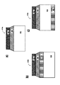
‐基板(111,112,113,114,115,211,212,213,311a〜311m,411,412,413)と、
‐前記基板上の、少なくとも1つの反射層系を有する積層体(121,122,123,124,125,221,222,223,321a〜321m,421,422,423)とを備え、
‐前記ミラー素子の曲率は、所定の動作温度に対する所望の意図される曲率に基づいて、前記積層体によってかけられる非消失の曲げ力によって生成され、
‐前記生成された曲率は、少なくとも10Kの温度間隔(ΔT)に亘って10%以下で変動し、
前記ミラー素子は、補償層(231,232,233,331a,331b,・・・)を備え、該補償層は、前記温度間隔(ΔT)内で生じる温度変化を伴う、前記積層体(221,222,223,321a,321b・・・)によってかけられる曲げ力の変動を、該曲げ力の前記ミラー素子の曲率への影響に関して、少なくとも部分的に補償し、
前記ミラー素子は、所望の機械的張力又は所望の曲げ力が前記積層体によって前記基板にかけられるように構成された張力誘導層(351b,351c,・・・;452,453)を更に備え、該張力誘導層は、前記基板により前記補償層から分離されるミラー素子。 - 請求項1に記載のミラー素子において、前記生成された曲率は、少なくとも10Kの温度間隔(ΔT)に亘って、1%以下で変動することを特徴とするミラー素子。
- 請求項1又は2に記載のミラー素子において、前記積層体(421,422,423)と前記基板(411,412,413)の間の機械的張力の伝達を低減する均等層(441,442,443)を備えることを特徴とするミラー素子。
- 請求項1〜3の何れか一項に記載のミラー素子において、前記基板(111,112,113,114,115)の平均熱膨張係数は第1の値を有し、前記積層体(121,122,123,124,125)の平均熱膨張係数は第2の値を有し、前記第1の値及び前記第2の値は、これら2つの値の内の大きい値に対して、±10%以内で対応することを特徴とするミラー素子。
- 請求項4に記載のミラー素子において、前記基板(112,113,114,115)は少なくとも2つの異なる熱膨張係数を有する材料によって構成されることを特徴とするミラー素子。
- 請求項1〜5の何れか一項に記載のミラー素子において、複数のミラー素子から構成されるミラー構成体のミラー素子であることを特徴とするミラー素子。
- 請求項6に記載のミラー素子において、相互に独立して傾斜可能であることを特徴とするミラー素子。
- 請求項6又は7に記載のミラー素子において、前記ミラー構成体はファセットミラーであることを特徴とするミラー素子。
- 請求項1〜8の何れか一項に記載のミラー素子において、30nm未満の動作波長用に設計されたものであることを特徴とするミラー素子。
- 請求項1〜9の何れか一項に記載のミラー素子において、マイクロリソグラフィ投影露光装置のミラー素子であることを特徴とするミラー素子。
- 請求項10に記載の少なくとも1つのミラー素子を備える、マイクロリソグラフィ投影露光装置の光学系。
- 照明デバイス及び投影レンズを備えるマイクロリソグラフィ投影露光装置であって、請求項11に記載の光学系を備えることを特徴とする投影露光装置。
Applications Claiming Priority (2)
| Application Number | Priority Date | Filing Date | Title |
|---|---|---|---|
| DE102015225510.7 | 2015-12-16 | ||
| DE102015225510.7A DE102015225510A1 (de) | 2015-12-16 | 2015-12-16 | Spiegelelement, insbesondere für eine mikrolithographische Projektionsbelichtungsanlage |
Publications (3)
| Publication Number | Publication Date |
|---|---|
| JP2017126062A JP2017126062A (ja) | 2017-07-20 |
| JP2017126062A5 JP2017126062A5 (ja) | 2020-01-30 |
| JP6875846B2 true JP6875846B2 (ja) | 2021-05-26 |
Family
ID=57584057
Family Applications (1)
| Application Number | Title | Priority Date | Filing Date |
|---|---|---|---|
| JP2016242654A Active JP6875846B2 (ja) | 2015-12-16 | 2016-12-14 | 特にマイクロリソグラフィ投影露光装置用のミラー素子 |
Country Status (3)
| Country | Link |
|---|---|
| US (2) | US20170176741A1 (ja) |
| JP (1) | JP6875846B2 (ja) |
| DE (1) | DE102015225510A1 (ja) |
Families Citing this family (1)
| Publication number | Priority date | Publication date | Assignee | Title |
|---|---|---|---|---|
| US20200201027A1 (en) * | 2018-12-21 | 2020-06-25 | Didi Research America, Llc | Micromachined mirror assembly having multiple coating layers |
Family Cites Families (18)
| Publication number | Priority date | Publication date | Assignee | Title |
|---|---|---|---|---|
| DE10314212B4 (de) | 2002-03-29 | 2010-06-02 | Hoya Corp. | Verfahren zur Herstellung eines Maskenrohlings, Verfahren zur Herstellung einer Transfermaske |
| US6994444B2 (en) | 2002-06-14 | 2006-02-07 | Asml Holding N.V. | Method and apparatus for managing actinic intensity transients in a lithography mirror |
| US6778315B2 (en) * | 2002-09-25 | 2004-08-17 | Rosemount Aerospace Inc. | Micro mirror structure with flat reflective coating |
| KR101159867B1 (ko) | 2003-09-12 | 2012-06-26 | 칼 짜이스 에스엠티 게엠베하 | 마이크로리소그래피 투사 노출 장치용 조명 시스템 |
| JP2007108194A (ja) * | 2005-10-11 | 2007-04-26 | Canon Inc | 多層膜ミラーの製造方法、光学系の製造方法、露光装置、及びデバイス製造方法 |
| KR20080066763A (ko) | 2005-11-10 | 2008-07-16 | 아사히 가라스 가부시키가이샤 | Euv 리소그래피용 반사형 마스크 블랭크의 다층반사막을 성막하는 방법 및 euv 리소그래피용 반사형마스크 블랭크의 제조 방법 |
| US7261430B1 (en) * | 2006-02-22 | 2007-08-28 | Teledyne Licensing, Llc | Thermal and intrinsic stress compensated micromirror apparatus and method |
| DE102006057568A1 (de) * | 2006-11-28 | 2008-05-29 | Micronic Laser Systems Ab | Mikrooptisches Element mit einem Substrat und Verfahren zu seiner Herstellung |
| DE102006057567B4 (de) | 2006-11-28 | 2008-09-04 | Micronic Laser Systems Ab | Mikrooptisches Element mit einem Substrat, an dem an einer optisch wirksamen Oberfläche mindestens eine Höhenstufe ausgebildet ist, Verfahren zu seiner Herstellung und Verwendungen |
| CN103293665B (zh) | 2008-02-15 | 2016-07-06 | 卡尔蔡司Smt有限责任公司 | 微光刻的投射曝光设备使用的分面镜 |
| DE102008009600A1 (de) | 2008-02-15 | 2009-08-20 | Carl Zeiss Smt Ag | Facettenspiegel zum Einsatz in einer Projektionsbelichtungsanlage für die Mikro-Lithographie |
| DE102008042212A1 (de) | 2008-09-19 | 2010-04-01 | Carl Zeiss Smt Ag | Reflektives optisches Element und Verfahren zu seiner Herstellung |
| JP5549222B2 (ja) * | 2009-12-28 | 2014-07-16 | 株式会社ニコン | 空間光変調器、露光装置およびそれらの製造方法 |
| DE102010028488A1 (de) | 2010-05-03 | 2011-11-03 | Carl Zeiss Smt Gmbh | Substrate für Spiegel für die EUV-Lithographie und deren Herstellung |
| DE102010017106A1 (de) * | 2010-05-27 | 2011-12-01 | Carl Zeiss Laser Optics Gmbh | Spiegel mit dielektrischer Beschichtung |
| DE102011003357A1 (de) | 2011-01-31 | 2012-08-02 | Carl Zeiss Smt Gmbh | Spiegel für den EUV-Wellenlängenbereich, Herstellungsverfahren für einen solchen Spiegel, Projektionsobjektiv für die Mikrolithographie mit einem solchen Spiegel und Projektionsbelichtungsanlage für die Mikrolithographie mit einem solchen Projektionsobjektiv |
| DE102014201622A1 (de) | 2014-01-30 | 2015-08-20 | Carl Zeiss Smt Gmbh | Verfahren zum Herstellen eines Spiegelelements |
| DE102015200328A1 (de) | 2015-01-13 | 2016-07-14 | Carl Zeiss Smt Gmbh | Verfahren zum Herstellen eines optischen Elements für ein optisches System, insbesondere für einemikrolithographische Projektionsbelichtungsanlage |
-
2015
- 2015-12-16 DE DE102015225510.7A patent/DE102015225510A1/de not_active Ceased
-
2016
- 2016-12-14 JP JP2016242654A patent/JP6875846B2/ja active Active
- 2016-12-16 US US15/381,910 patent/US20170176741A1/en not_active Abandoned
-
2017
- 2017-12-11 US US15/837,932 patent/US10598921B2/en active Active
Also Published As
| Publication number | Publication date |
|---|---|
| US10598921B2 (en) | 2020-03-24 |
| US20170176741A1 (en) | 2017-06-22 |
| US20180101002A1 (en) | 2018-04-12 |
| JP2017126062A (ja) | 2017-07-20 |
| DE102015225510A1 (de) | 2017-01-12 |
Similar Documents
| Publication | Publication Date | Title |
|---|---|---|
| US9798254B2 (en) | Arrangement for the thermal actuation of a mirror, in particular in a microlithographic projection exposure apparatus | |
| JP5487110B2 (ja) | マイクロリソグラフィ投影露光装置 | |
| US9785054B2 (en) | Mirror, more particularly for a microlithographic projection exposure apparatus | |
| KR101288782B1 (ko) | Uv 또는 euv 리소그래피용 광학 소자 | |
| JP2002520601A (ja) | EUVのためのSiO2被覆したミラー基板 | |
| US10423073B2 (en) | Method for producing a mirror element | |
| TW201022854A (en) | Illumination system of a microlithographic projection exposure apparatus | |
| JP6399889B2 (ja) | 反射光学素子 | |
| US11187990B2 (en) | Mirror for a microlithographic projection exposure apparatus, and method for operating a deformable mirror | |
| TWI684069B (zh) | 微影投射曝光裝置之光學配置 | |
| JP2010533370A (ja) | マイクロリソグラフィ投影露光装置の光学システム | |
| US20170315452A1 (en) | Method For Producing An Optical Element For An Optical System, In Particular For A Microlithographic Projection Exposure Apparatus | |
| US20180059413A1 (en) | Wavefront correction element for use in an optical system | |
| JP6875846B2 (ja) | 特にマイクロリソグラフィ投影露光装置用のミラー素子 | |
| TW202328826A (zh) | 投射微影中用於成像光之光束導引的光學元件 | |
| TW201543137A (zh) | 光刻之光罩 | |
| CN114072731A (zh) | 产生第一部件与第二部件之间的粘合接合的方法和装置 | |
| KR20210035181A (ko) | 마이크로리소그래피용 광학 시스템에서 광학 요소의 가열 상태를 결정하기 위한 방법 및 디바이스 | |
| US7522260B1 (en) | Method for correcting astigmatism in a microlithography projection exposure apparatus, a projection objective of such a projection exposure apparatus, and a fabrication method for micropatterned components | |
| TW202210953A (zh) | 反射鏡、特別是用於微影投射曝光裝置的反射鏡 | |
| JP6862154B2 (ja) | 光学素子、露光装置、および物品の製造方法 | |
| JP2024507881A (ja) | 光学アセンブリ、光学素子を変形させる方法、及び投影露光システム | |
| JP2023530521A (ja) | 特にマイクロリソグラフィ投影露光装置のミラー | |
| KR20200106903A (ko) | 투영 리소그래피에서의 결상 광의 빔 안내를 위한 광학 요소 |
Legal Events
| Date | Code | Title | Description |
|---|---|---|---|
| A521 | Request for written amendment filed |
Free format text: JAPANESE INTERMEDIATE CODE: A523 Effective date: 20191212 |
|
| A621 | Written request for application examination |
Free format text: JAPANESE INTERMEDIATE CODE: A621 Effective date: 20191212 |
|
| A977 | Report on retrieval |
Free format text: JAPANESE INTERMEDIATE CODE: A971007 Effective date: 20201009 |
|
| A131 | Notification of reasons for refusal |
Free format text: JAPANESE INTERMEDIATE CODE: A131 Effective date: 20201020 |
|
| A521 | Request for written amendment filed |
Free format text: JAPANESE INTERMEDIATE CODE: A523 Effective date: 20201221 |
|
| TRDD | Decision of grant or rejection written | ||
| A01 | Written decision to grant a patent or to grant a registration (utility model) |
Free format text: JAPANESE INTERMEDIATE CODE: A01 Effective date: 20210413 |
|
| A61 | First payment of annual fees (during grant procedure) |
Free format text: JAPANESE INTERMEDIATE CODE: A61 Effective date: 20210423 |
|
| R150 | Certificate of patent or registration of utility model |
Ref document number: 6875846 Country of ref document: JP Free format text: JAPANESE INTERMEDIATE CODE Ref document number: 6875846 Country of ref document: JP Free format text: JAPANESE INTERMEDIATE CODE: R150 |
|
| R250 | Receipt of annual fees |
Free format text: JAPANESE INTERMEDIATE CODE: R250 |