JP6875846B2 - Mirror elements especially for microlithography projection exposure equipment - Google Patents
Mirror elements especially for microlithography projection exposure equipment Download PDFInfo
- Publication number
- JP6875846B2 JP6875846B2 JP2016242654A JP2016242654A JP6875846B2 JP 6875846 B2 JP6875846 B2 JP 6875846B2 JP 2016242654 A JP2016242654 A JP 2016242654A JP 2016242654 A JP2016242654 A JP 2016242654A JP 6875846 B2 JP6875846 B2 JP 6875846B2
- Authority
- JP
- Japan
- Prior art keywords
- mirror
- mirror element
- substrate
- laminate
- curvature
- Prior art date
- Legal status (The legal status is an assumption and is not a legal conclusion. Google has not performed a legal analysis and makes no representation as to the accuracy of the status listed.)
- Active
Links
- 238000001393 microlithography Methods 0.000 title claims description 12
- 239000000758 substrate Substances 0.000 claims description 83
- 238000005452 bending Methods 0.000 claims description 27
- 239000000463 material Substances 0.000 claims description 17
- 230000003287 optical effect Effects 0.000 claims description 10
- 238000005286 illumination Methods 0.000 claims description 9
- 230000006698 induction Effects 0.000 claims description 7
- 230000005540 biological transmission Effects 0.000 claims description 2
- 229960001716 benzalkonium Drugs 0.000 claims 1
- CYDRXTMLKJDRQH-UHFFFAOYSA-N benzododecinium Chemical compound CCCCCCCCCCCC[N+](C)(C)CC1=CC=CC=C1 CYDRXTMLKJDRQH-UHFFFAOYSA-N 0.000 claims 1
- 239000010410 layer Substances 0.000 description 54
- 230000000694 effects Effects 0.000 description 14
- 239000011248 coating agent Substances 0.000 description 11
- 238000000576 coating method Methods 0.000 description 11
- 238000000034 method Methods 0.000 description 10
- 210000001747 pupil Anatomy 0.000 description 9
- XUIMIQQOPSSXEZ-UHFFFAOYSA-N Silicon Chemical compound [Si] XUIMIQQOPSSXEZ-UHFFFAOYSA-N 0.000 description 7
- 229910052710 silicon Inorganic materials 0.000 description 7
- 239000010703 silicon Substances 0.000 description 7
- 238000010586 diagram Methods 0.000 description 5
- 238000004519 manufacturing process Methods 0.000 description 5
- 239000000203 mixture Substances 0.000 description 4
- VYPSYNLAJGMNEJ-UHFFFAOYSA-N Silicium dioxide Chemical compound O=[Si]=O VYPSYNLAJGMNEJ-UHFFFAOYSA-N 0.000 description 3
- 238000013461 design Methods 0.000 description 3
- 229910052732 germanium Inorganic materials 0.000 description 3
- GNPVGFCGXDBREM-UHFFFAOYSA-N germanium atom Chemical compound [Ge] GNPVGFCGXDBREM-UHFFFAOYSA-N 0.000 description 3
- OAICVXFJPJFONN-UHFFFAOYSA-N Phosphorus Chemical compound [P] OAICVXFJPJFONN-UHFFFAOYSA-N 0.000 description 2
- QVGXLLKOCUKJST-UHFFFAOYSA-N atomic oxygen Chemical compound [O] QVGXLLKOCUKJST-UHFFFAOYSA-N 0.000 description 2
- 230000015572 biosynthetic process Effects 0.000 description 2
- 239000002346 layers by function Substances 0.000 description 2
- 229910052760 oxygen Inorganic materials 0.000 description 2
- 239000001301 oxygen Substances 0.000 description 2
- 229910052698 phosphorus Inorganic materials 0.000 description 2
- 239000011574 phosphorus Substances 0.000 description 2
- 229920002120 photoresistant polymer Polymers 0.000 description 2
- 238000000926 separation method Methods 0.000 description 2
- 238000012546 transfer Methods 0.000 description 2
- 229910018072 Al 2 O 3 Inorganic materials 0.000 description 1
- 241000370685 Arge Species 0.000 description 1
- JBRZTFJDHDCESZ-UHFFFAOYSA-N AsGa Chemical compound [As]#[Ga] JBRZTFJDHDCESZ-UHFFFAOYSA-N 0.000 description 1
- 229910005542 GaSb Inorganic materials 0.000 description 1
- GYHNNYVSQQEPJS-UHFFFAOYSA-N Gallium Chemical compound [Ga] GYHNNYVSQQEPJS-UHFFFAOYSA-N 0.000 description 1
- JMASRVWKEDWRBT-UHFFFAOYSA-N Gallium nitride Chemical compound [Ga]#N JMASRVWKEDWRBT-UHFFFAOYSA-N 0.000 description 1
- GPXJNWSHGFTCBW-UHFFFAOYSA-N Indium phosphide Chemical compound [In]#P GPXJNWSHGFTCBW-UHFFFAOYSA-N 0.000 description 1
- ZOKXTWBITQBERF-UHFFFAOYSA-N Molybdenum Chemical compound [Mo] ZOKXTWBITQBERF-UHFFFAOYSA-N 0.000 description 1
- 229910004298 SiO 2 Inorganic materials 0.000 description 1
- GWEVSGVZZGPLCZ-UHFFFAOYSA-N Titan oxide Chemical compound O=[Ti]=O GWEVSGVZZGPLCZ-UHFFFAOYSA-N 0.000 description 1
- 239000006094 Zerodur Substances 0.000 description 1
- XLOMVQKBTHCTTD-UHFFFAOYSA-N Zinc monoxide Chemical compound [Zn]=O XLOMVQKBTHCTTD-UHFFFAOYSA-N 0.000 description 1
- 230000002745 absorbent Effects 0.000 description 1
- 239000002250 absorbent Substances 0.000 description 1
- 230000006978 adaptation Effects 0.000 description 1
- 229910045601 alloy Inorganic materials 0.000 description 1
- 239000000956 alloy Substances 0.000 description 1
- 229910052782 aluminium Inorganic materials 0.000 description 1
- XAGFODPZIPBFFR-UHFFFAOYSA-N aluminium Chemical compound [Al] XAGFODPZIPBFFR-UHFFFAOYSA-N 0.000 description 1
- WUKWITHWXAAZEY-UHFFFAOYSA-L calcium difluoride Chemical compound [F-].[F-].[Ca+2] WUKWITHWXAAZEY-UHFFFAOYSA-L 0.000 description 1
- 230000015556 catabolic process Effects 0.000 description 1
- 238000006731 degradation reaction Methods 0.000 description 1
- 230000001419 dependent effect Effects 0.000 description 1
- 230000006866 deterioration Effects 0.000 description 1
- 239000010432 diamond Substances 0.000 description 1
- 229910003460 diamond Inorganic materials 0.000 description 1
- 229910052733 gallium Inorganic materials 0.000 description 1
- VTGARNNDLOTBET-UHFFFAOYSA-N gallium antimonide Chemical compound [Sb]#[Ga] VTGARNNDLOTBET-UHFFFAOYSA-N 0.000 description 1
- 238000003384 imaging method Methods 0.000 description 1
- WPYVAWXEWQSOGY-UHFFFAOYSA-N indium antimonide Chemical compound [Sb]#[In] WPYVAWXEWQSOGY-UHFFFAOYSA-N 0.000 description 1
- RPQDHPTXJYYUPQ-UHFFFAOYSA-N indium arsenide Chemical compound [In]#[As] RPQDHPTXJYYUPQ-UHFFFAOYSA-N 0.000 description 1
- 238000005259 measurement Methods 0.000 description 1
- 238000012986 modification Methods 0.000 description 1
- 230000004048 modification Effects 0.000 description 1
- 229910052750 molybdenum Inorganic materials 0.000 description 1
- 239000011733 molybdenum Substances 0.000 description 1
- 239000011241 protective layer Substances 0.000 description 1
- HBMJWWWQQXIZIP-UHFFFAOYSA-N silicon carbide Chemical compound [Si+]#[C-] HBMJWWWQQXIZIP-UHFFFAOYSA-N 0.000 description 1
- 235000012239 silicon dioxide Nutrition 0.000 description 1
- 239000000377 silicon dioxide Substances 0.000 description 1
Images


Classifications
-
- G—PHYSICS
- G02—OPTICS
- G02B—OPTICAL ELEMENTS, SYSTEMS OR APPARATUS
- G02B26/00—Optical devices or arrangements for the control of light using movable or deformable optical elements
- G02B26/08—Optical devices or arrangements for the control of light using movable or deformable optical elements for controlling the direction of light
- G02B26/0816—Optical devices or arrangements for the control of light using movable or deformable optical elements for controlling the direction of light by means of one or more reflecting elements
- G02B26/0833—Optical devices or arrangements for the control of light using movable or deformable optical elements for controlling the direction of light by means of one or more reflecting elements the reflecting element being a micromechanical device, e.g. a MEMS mirror, DMD
-
- G—PHYSICS
- G02—OPTICS
- G02B—OPTICAL ELEMENTS, SYSTEMS OR APPARATUS
- G02B7/00—Mountings, adjusting means, or light-tight connections, for optical elements
- G02B7/18—Mountings, adjusting means, or light-tight connections, for optical elements for prisms; for mirrors
- G02B7/181—Mountings, adjusting means, or light-tight connections, for optical elements for prisms; for mirrors with means for compensating for changes in temperature or for controlling the temperature; thermal stabilisation
-
- G—PHYSICS
- G02—OPTICS
- G02B—OPTICAL ELEMENTS, SYSTEMS OR APPARATUS
- G02B5/00—Optical elements other than lenses
- G02B5/08—Mirrors
- G02B5/0816—Multilayer mirrors, i.e. having two or more reflecting layers
-
- G—PHYSICS
- G02—OPTICS
- G02B—OPTICAL ELEMENTS, SYSTEMS OR APPARATUS
- G02B5/00—Optical elements other than lenses
- G02B5/08—Mirrors
- G02B5/0891—Ultraviolet [UV] mirrors
-
- G—PHYSICS
- G02—OPTICS
- G02B—OPTICAL ELEMENTS, SYSTEMS OR APPARATUS
- G02B5/00—Optical elements other than lenses
- G02B5/08—Mirrors
- G02B5/09—Multifaceted or polygonal mirrors, e.g. polygonal scanning mirrors; Fresnel mirrors
-
- G—PHYSICS
- G02—OPTICS
- G02B—OPTICAL ELEMENTS, SYSTEMS OR APPARATUS
- G02B5/00—Optical elements other than lenses
- G02B5/08—Mirrors
- G02B5/10—Mirrors with curved faces
-
- G—PHYSICS
- G03—PHOTOGRAPHY; CINEMATOGRAPHY; ANALOGOUS TECHNIQUES USING WAVES OTHER THAN OPTICAL WAVES; ELECTROGRAPHY; HOLOGRAPHY
- G03F—PHOTOMECHANICAL PRODUCTION OF TEXTURED OR PATTERNED SURFACES, e.g. FOR PRINTING, FOR PROCESSING OF SEMICONDUCTOR DEVICES; MATERIALS THEREFOR; ORIGINALS THEREFOR; APPARATUS SPECIALLY ADAPTED THEREFOR
- G03F7/00—Photomechanical, e.g. photolithographic, production of textured or patterned surfaces, e.g. printing surfaces; Materials therefor, e.g. comprising photoresists; Apparatus specially adapted therefor
- G03F7/70—Microphotolithographic exposure; Apparatus therefor
- G03F7/70058—Mask illumination systems
- G03F7/70075—Homogenization of illumination intensity in the mask plane by using an integrator, e.g. fly's eye lens, facet mirror or glass rod, by using a diffusing optical element or by beam deflection
-
- G—PHYSICS
- G03—PHOTOGRAPHY; CINEMATOGRAPHY; ANALOGOUS TECHNIQUES USING WAVES OTHER THAN OPTICAL WAVES; ELECTROGRAPHY; HOLOGRAPHY
- G03F—PHOTOMECHANICAL PRODUCTION OF TEXTURED OR PATTERNED SURFACES, e.g. FOR PRINTING, FOR PROCESSING OF SEMICONDUCTOR DEVICES; MATERIALS THEREFOR; ORIGINALS THEREFOR; APPARATUS SPECIALLY ADAPTED THEREFOR
- G03F7/00—Photomechanical, e.g. photolithographic, production of textured or patterned surfaces, e.g. printing surfaces; Materials therefor, e.g. comprising photoresists; Apparatus specially adapted therefor
- G03F7/70—Microphotolithographic exposure; Apparatus therefor
- G03F7/70058—Mask illumination systems
- G03F7/70091—Illumination settings, i.e. intensity distribution in the pupil plane or angular distribution in the field plane; On-axis or off-axis settings, e.g. annular, dipole or quadrupole settings; Partial coherence control, i.e. sigma or numerical aperture [NA]
- G03F7/70116—Off-axis setting using a programmable means, e.g. liquid crystal display [LCD], digital micromirror device [DMD] or pupil facets
-
- G—PHYSICS
- G03—PHOTOGRAPHY; CINEMATOGRAPHY; ANALOGOUS TECHNIQUES USING WAVES OTHER THAN OPTICAL WAVES; ELECTROGRAPHY; HOLOGRAPHY
- G03F—PHOTOMECHANICAL PRODUCTION OF TEXTURED OR PATTERNED SURFACES, e.g. FOR PRINTING, FOR PROCESSING OF SEMICONDUCTOR DEVICES; MATERIALS THEREFOR; ORIGINALS THEREFOR; APPARATUS SPECIALLY ADAPTED THEREFOR
- G03F7/00—Photomechanical, e.g. photolithographic, production of textured or patterned surfaces, e.g. printing surfaces; Materials therefor, e.g. comprising photoresists; Apparatus specially adapted therefor
- G03F7/70—Microphotolithographic exposure; Apparatus therefor
- G03F7/70058—Mask illumination systems
- G03F7/7015—Details of optical elements
-
- G—PHYSICS
- G03—PHOTOGRAPHY; CINEMATOGRAPHY; ANALOGOUS TECHNIQUES USING WAVES OTHER THAN OPTICAL WAVES; ELECTROGRAPHY; HOLOGRAPHY
- G03F—PHOTOMECHANICAL PRODUCTION OF TEXTURED OR PATTERNED SURFACES, e.g. FOR PRINTING, FOR PROCESSING OF SEMICONDUCTOR DEVICES; MATERIALS THEREFOR; ORIGINALS THEREFOR; APPARATUS SPECIALLY ADAPTED THEREFOR
- G03F7/00—Photomechanical, e.g. photolithographic, production of textured or patterned surfaces, e.g. printing surfaces; Materials therefor, e.g. comprising photoresists; Apparatus specially adapted therefor
- G03F7/70—Microphotolithographic exposure; Apparatus therefor
- G03F7/70216—Mask projection systems
- G03F7/70316—Details of optical elements, e.g. of Bragg reflectors, extreme ultraviolet [EUV] multilayer or bilayer mirrors or diffractive optical elements
-
- G—PHYSICS
- G03—PHOTOGRAPHY; CINEMATOGRAPHY; ANALOGOUS TECHNIQUES USING WAVES OTHER THAN OPTICAL WAVES; ELECTROGRAPHY; HOLOGRAPHY
- G03F—PHOTOMECHANICAL PRODUCTION OF TEXTURED OR PATTERNED SURFACES, e.g. FOR PRINTING, FOR PROCESSING OF SEMICONDUCTOR DEVICES; MATERIALS THEREFOR; ORIGINALS THEREFOR; APPARATUS SPECIALLY ADAPTED THEREFOR
- G03F7/00—Photomechanical, e.g. photolithographic, production of textured or patterned surfaces, e.g. printing surfaces; Materials therefor, e.g. comprising photoresists; Apparatus specially adapted therefor
- G03F7/70—Microphotolithographic exposure; Apparatus therefor
- G03F7/708—Construction of apparatus, e.g. environment aspects, hygiene aspects or materials
- G03F7/70858—Environment aspects, e.g. pressure of beam-path gas, temperature
- G03F7/70883—Environment aspects, e.g. pressure of beam-path gas, temperature of optical system
- G03F7/70891—Temperature
-
- G—PHYSICS
- G03—PHOTOGRAPHY; CINEMATOGRAPHY; ANALOGOUS TECHNIQUES USING WAVES OTHER THAN OPTICAL WAVES; ELECTROGRAPHY; HOLOGRAPHY
- G03F—PHOTOMECHANICAL PRODUCTION OF TEXTURED OR PATTERNED SURFACES, e.g. FOR PRINTING, FOR PROCESSING OF SEMICONDUCTOR DEVICES; MATERIALS THEREFOR; ORIGINALS THEREFOR; APPARATUS SPECIALLY ADAPTED THEREFOR
- G03F7/00—Photomechanical, e.g. photolithographic, production of textured or patterned surfaces, e.g. printing surfaces; Materials therefor, e.g. comprising photoresists; Apparatus specially adapted therefor
- G03F7/70—Microphotolithographic exposure; Apparatus therefor
- G03F7/708—Construction of apparatus, e.g. environment aspects, hygiene aspects or materials
- G03F7/7095—Materials, e.g. materials for housing, stage or other support having particular properties, e.g. weight, strength, conductivity, thermal expansion coefficient
- G03F7/70958—Optical materials or coatings, e.g. with particular transmittance, reflectance or anti-reflection properties
Landscapes
- Physics & Mathematics (AREA)
- General Physics & Mathematics (AREA)
- Optics & Photonics (AREA)
- Health & Medical Sciences (AREA)
- Epidemiology (AREA)
- Engineering & Computer Science (AREA)
- Environmental & Geological Engineering (AREA)
- Public Health (AREA)
- Atmospheric Sciences (AREA)
- Toxicology (AREA)
- Life Sciences & Earth Sciences (AREA)
- Optical Elements Other Than Lenses (AREA)
- Exposure And Positioning Against Photoresist Photosensitive Materials (AREA)
Description
本発明は、特にマイクロリソグラフィ投影露光装置用のミラー素子に関する。 The present invention particularly relates to a mirror element for a microlithography projection exposure apparatus.
マイクロリソグラフィは、例えば集積回路又はLCDなどの微細構造部品の製造に使用される。マイクロリソグラフィプロセスは、照明デバイス及び投影レンズを備える、いわゆる投影露光装置で行われる。照明デバイスによって照射されたマスク(レチクル)の像は、この場合、感光層(フォトレジスト)によってコーティングされ、投影レンズの像面に配置された基板(例えばシリコンウエハ)上に投影レンズによって投影され、マスク構造が基板の感光性コーティングに転写される。 Microlithography is used in the manufacture of microstructured components such as integrated circuits or LCDs. The microlithography process is carried out in a so-called projection exposure apparatus including an illumination device and a projection lens. The image of the mask (reticle) illuminated by the illumination device is, in this case, coated with a photosensitive layer (photoresist) and projected by the projection lens onto a substrate (eg, a silicon wafer) placed on the image plane of the projection lens. The mask structure is transferred to the photosensitive coating on the substrate.
EUV領域、すなわち、例えばおよそ13nm又はおよそ7nmの波長用に設計された投影レンズにおいて、適切な光透過性屈折材料がないため、結像工程の光学部品としてミラーが使用される。 In the EUV region, ie, projection lenses designed for wavelengths of about 13 nm or about 7 nm, mirrors are used as optics in the imaging process due to the lack of suitable light transmissive refracting materials.
EUV領域で動作させるために設計されたマイクロリソグラフィ投影露光装置の照明デバイスにおいて、集束部品として特にファセットミラーを視野ファセットミラー及び瞳ファセットミラーの形態で使用することは、例えば、特許文献1(ドイツ国特許出願第10 2008 009 600号明細書)より周知である。このようなファセットミラーは、特定の照射角度分布を調整、又は実現するために、各々が屈曲ベアリングによって傾斜可能に設計された、多数のミラーまたはミラーファセットより構成される。そしてこれらのミラーファセットは複数のマイクロミラーを備えることができる。 In the illumination device of a microlithography projection exposure apparatus designed to operate in the EUV region, the use of a facet mirror as a focusing component in the form of a field facet mirror and a pupil facet mirror is described, for example, in Patent Document 1 (Germany). It is well known from Patent Application No. 10 2008 009 600). Such faceted mirrors consist of a large number of mirrors or mirror facets, each designed to be tiltable by bending bearings in order to adjust or achieve a particular irradiation angle distribution. And these mirror facets can include a plurality of micromirrors.
更に、規定の照明設定(すなわち、照明デバイスの瞳面における輝度分布)を調整するための、VUV領域の波長で動作させるために設計されたマイクロリソグラフィ投影露光装置の照明デバイスにおいて、相互に独立して調整可能な複数のミラー素子を備えるミラー構成体の使用も、例えば特許文献2(国際公開第2005/026843 A2号パンフレット)より周知である。 In addition, they are mutually independent in the illumination devices of microlithographic projection exposure devices designed to operate at wavelengths in the VUV region for adjusting defined illumination settings (ie, the brightness distribution in the pupil plane of the illumination device). The use of a mirror structure including a plurality of adjustable mirror elements is also well known, for example, from Patent Document 2 (International Publication No. 2005/026843 A2 pamphlet).
実際にミラー素子を製造する際、その屈折力をそれぞれ可及的正確に調整する必要性があり、屈折力は、用途に応じて(平面鏡素子に対応して)ゼロ、又はゼロとは異なる屈折力とすることができる。これに関する周知の手法は、各ミラー素子を製造する際、反射層系を含む積層体を基板上に適用する際に生成される機械的張力、及びその結果積層体によって基板にかけられる曲げ力を、ミラー素子の所望の意図される曲率に意図的に使用し、それによってミラー素子の所望の最終的な屈折力を生成することからなる(この場合、基板は、積層体を形成する前のミラー素子における所望の意図される曲率とは異なる曲率を有する)。 When actually manufacturing a mirror element, it is necessary to adjust the refractive power as accurately as possible, and the refractive power is zero or different from zero depending on the application (corresponding to the plane mirror element). Can be a force. A well-known method for this is to apply the mechanical tension generated when a laminate including a reflective layer system is applied onto a substrate when manufacturing each mirror element, and the bending force applied to the substrate by the laminate as a result. It consists of deliberately using it for the desired intended curvature of the mirror element, thereby producing the desired final refractive power of the mirror element (in this case, the substrate is the mirror element before forming the laminate). Has a curvature different from the desired intended curvature in).
実際、ミラー素子が(起動中及びその後の各光学系の作動中)温度変化にさらされ、これは、(すなわちいわゆるバイメタリック効果の結果として)積層体と基板とで熱膨張が異なる場合、各ミラー素子の曲率又は屈折力に望ましくない変化を生じさせ、その結果、ミラー素子を備える光学系の光学特性の劣化がもたらされるという問題が発生する。 In fact, the mirror element is exposed to temperature changes (during startup and subsequent operation of each optical system), which is the case when the laminate and the substrate have different thermal expansions (ie, as a result of the so-called bimetallic effect). The problem arises that the curvature or refractive power of the mirror element is undesirably changed, resulting in deterioration of the optical properties of the optical system including the mirror element.
先行技術に関しては、特許文献3(国際公開第2015/114043 A1号パンフレット)、特許文献4(ドイツ国特許出願第10 2010 028 488号明細書)及び特許文献5(ドイツ国特許出願第10 2006 057 567号明細書)を単なる例として参照する。 Regarding the prior art, Patent Document 3 (International Publication No. 2015/114043 A1 pamphlet), Patent Document 4 (German Patent Application No. 10 2010 028 488) and Patent Document 5 (German Patent Application No. 10 2006 057). 567) is referred to as a mere example.
本発明の目的は、作動中に温度変化が発生した場合、熱的に誘導されるミラー素子の屈折力の変化を少なくとも低減させるミラー素子を提供することである。 An object of the present invention is to provide a mirror element that at least reduces a change in the refractive power of the mirror element that is thermally induced when a temperature change occurs during operation.
この目的は独立請求項の特徴に従ったミラー素子によって達成される。 This object is achieved by a mirror element according to the characteristics of the independent claims.
本発明の一態様によれば、本発明による、特にマイクロリソグラフィ投影露光装置用のミラー素子は、
‐基板と、
‐基板上の、少なくとも1つの反射層系を有する積層体とを備え、
‐ミラー素子の曲率は、所定の動作温度に対する所望の意図される曲率に基づいて、積層体によってかけられる非消失の曲げ力によって生成され、
‐生成された曲率は、少なくとも10Kの温度間隔に亘って10%以下で変化する。
According to one aspect of the present invention, the mirror element according to the present invention, particularly for a microlithography projection exposure apparatus, is
-Board and
-With a laminate having at least one reflective layer system on the substrate,
-The curvature of the mirror element is generated by the non-disappearing bending force applied by the laminate based on the desired intended curvature for a given operating temperature.
-The generated curvature varies by less than 10% over a temperature interval of at least 10K.
本態様によれば、本発明は元来、反射層系を含む積層体を基板に適用する際に発生する機械的張力と、その結果積層体によって基板にかけられる曲げ力とを意図的に使用して、ミラー素子の所望の意図される曲率又は屈折力を生成するという原理から生じたものである(この場合、基板は、積層体の形成前の、ミラー素子の所望の意図される曲率とは異なる曲率を有する)。 According to this aspect, the present invention originally intentionally uses the mechanical tension generated when applying the laminate including the reflective layer system to the substrate and the bending force applied to the substrate by the laminate as a result. Thus, it arises from the principle of generating the desired intended curvature or refractive power of the mirror element (in this case, the substrate is the desired intended curvature of the mirror element before the formation of the laminate. Has different curvatures).
そして本発明は、基板及び積層体で構成される(全)システムを、少なくとも限られた温度間隔内で温度変化が発生する場合であっても、ミラー素子の曲率の大きな変動やそれによるミラー素子の屈折力の大きな変動がないように設計する、すなわち、少なくとも制限された温度範囲に亘って、望ましくないバイメタリック効果が大幅に回避されるように設計するという概念に基づくものである。 The present invention relates to a (whole) system composed of a substrate and a laminate, even when a temperature change occurs at least within a limited temperature interval, a large fluctuation in the curvature of the mirror element and the resulting mirror element. It is based on the concept of designing so that there are no large fluctuations in the refractive power of the mirror, that is, designing so that unwanted bimetallic effects are largely avoided, at least over a limited temperature range.
一実施形態によれば、発生した曲率は、少なくとも10Kの温度間隔(ΔT)に亘って1%以下、特に0.1%以下で変化する。 According to one embodiment, the generated curvature varies by 1% or less, especially 0.1% or less, over a temperature interval (ΔT) of at least 10K.
一実施形態によれば、ミラー素子は補償層を備え、これは、温度間隔内で発生する、積層体によってかけられる温度変化を伴う曲げ力の変動を、この曲げ力のミラー素子の曲率への影響に関して、少なくとも部分的に補償する。従って、本手法によれば、本発明によるバイメタリック効果の補償は、この目的のために提供される追加層によって実行され、この追加層は、全体構造の中でのこの追加層の基板及び積層体に対する配置に応じて、曲げ力を基板にかけるだけであり、この曲げ力は、温度変化によって更に誘発される積層体の曲げ力と比較すると、同じ強さ又は反対符合で(opposite sign)同じ強さであり、理想的には、積層体の曲げ力の熱的に誘導される変化が補償され、曲率又は屈折力の熱的に誘導される変化がシステム全体又はミラー素子においてそれ以上発生しない。 According to one embodiment, the mirror element comprises a compensating layer, which causes fluctuations in bending force with temperature changes applied by the laminate, which occur within a temperature interval, to the curvature of the mirror element of this bending force. Compensate at least partially for the impact. Therefore, according to the method, compensation for the bimetallic effect according to the present invention is carried out by an additional layer provided for this purpose, which additional layer is the substrate and laminate of this additional layer in the overall structure. Depending on the placement on the body, only a bending force is applied to the substrate, which is the same strength or opposite sign when compared to the bending force of the laminate further induced by temperature changes. Strength, ideally compensated for thermally induced changes in the bending force of the laminate, with no further thermally induced changes in curvature or refractive power occurring throughout the system or in the mirror element. ..
一実施形態によれば、ミラー素子は均等層を備え、これは、均等層を備えていない類似の構成と比較すると、積層体と基板との間の機械的張力の伝達を低減する。従ってこの手法によれば、本発明によるバイメタリック効果の補償は、「ソフトな」均等層によって提供される積層体と基板との間の機械的分離によってもたらされる。 According to one embodiment, the mirror element comprises a uniform layer, which reduces the transfer of mechanical tension between the laminate and the substrate as compared to a similar configuration without the uniform layer. Therefore, according to this technique, compensation for the bimetallic effect according to the invention is provided by the mechanical separation between the laminate and the substrate provided by the "soft" even layer.
一実施形態によれば、ミラー素子は、基板の平均熱膨張係数が第1の値を有し、積層体の平均熱膨張係数が第2の値を有するように構成され、これら第1の値及び第2の値は、2つの値の内の大きな方に対して、±10%以下、特に±3%以下、更に特に±1%以下である。 According to one embodiment, the mirror element is configured such that the average coefficient of thermal expansion of the substrate has a first value and the average coefficient of thermal expansion of the laminate has a second value, these first values. The second value is ± 10% or less, particularly ± 3% or less, and more particularly ± 1% or less with respect to the larger of the two values.
従って本手法によれば、本発明によるバイメタリック効果の補償は、基板の構成を、基板に使用される材料を考慮して、積層体の構成に、それぞれの平均熱膨張係数に関して調整することによって行われる。 Therefore, according to the present method, the compensation for the bimetallic effect according to the present invention is made by adjusting the composition of the substrate to the composition of the laminate in consideration of the material used for the substrate with respect to the respective average coefficient of thermal expansion. Will be done.
一実施形態によれば、基板は少なくとも2つの異なる材料から製造される。 According to one embodiment, the substrate is made from at least two different materials.
本発明は、最初に記載した、積層体によって基板にかけられる曲げ力を意図的に使用して、ミラー素子の所望の意図される曲率又は屈折力を生成させるという原理(この場合、基板は、積層体を形成する前の、ミラー素子の所望の意図される曲率とは異なる曲率を有する)の適用に制限されるのではなく、基板が最初からほぼ所望の意図される曲率で製造されているミラー素子にも適用することができる。この場合、積層体によって基板にかけられる曲げ力は、(例えば基板が比較的厚いため)非常に小さい。これは、(本発明に従って補償される)積層体と基板の異なる熱膨張による影響、又はそれによって発生するミラー素子の曲率又は屈折力の望ましくない変化の影響が、最初に記載された、例えば、視野ファセットミラー又は瞳ファセットミラーなどのファセットミラーのミラー素子を含む用途において、例えばマイクロリソグラフィ投影露光装置の動作中に光学特性の著しい低下をもたらすほど十分に深刻なままだからである。 The present invention is based on the principle described first, that the bending force applied to the substrate by the laminate is intentionally used to generate the desired intended curvature or refractive power of the mirror element (in this case, the substrate is laminated). Rather than being limited to the application of (having a curvature different from the desired intended curvature of the mirror element) before forming the body, the mirror from which the substrate is manufactured from the beginning with a near desired intended curvature. It can also be applied to elements. In this case, the bending force applied to the substrate by the laminate is very small (for example, because the substrate is relatively thick). This is because the effects of different thermal expansions of the laminate and the substrate (compensated according to the present invention), or the effects of undesired changes in the curvature or refractive power of the mirror element caused by it, were first described, eg, This is because applications including mirror elements of facet mirrors such as field facet mirrors or pupil facet mirrors remain serious enough to cause significant degradation of optical properties, for example during the operation of microlithographic projection exposure equipment.
従って本発明は更に、特にマイクロリソグラフィ投影露光装置用のミラー素子に関し、これは、
‐基板と、
‐基板上の、少なくとも1つの反射層系を有する積層体と、
‐均等層のない同等の設計と比較して、積層体と基板との間の機械的張力の伝達を低減させる均等層とを備える。
Therefore, the present invention further relates to mirror elements, especially for microlithographic projection exposure devices.
-Board and
-With a laminate having at least one reflective layer system on the substrate,
-Has an even layer that reduces the transfer of mechanical tension between the laminate and the substrate compared to an equivalent design without an even layer.
一実施形態によれば、ミラー素子は追加の張力誘導層を備える。この追加の張力誘導層は、所望の機械的張力又は積層体によって基板にかけられる所望の曲げ力が、最終的に達成されるように構成することができる。 According to one embodiment, the mirror element comprises an additional tension induction layer. This additional tension induction layer can be configured such that the desired mechanical tension or desired bending force applied to the substrate by the laminate is ultimately achieved.
一実施形態によれば、ミラー素子は複数のミラー素子から成るミラー構成体のミラー素子である。具体的には、これらのミラー素子は相互に独立して傾斜可能である。 According to one embodiment, the mirror element is a mirror element of a mirror structure composed of a plurality of mirror elements. Specifically, these mirror elements can be tilted independently of each other.
原理上、本発明は各ミラー素子の特定の寸法に制限されない。よってミラー素子は、例えば、いわゆるMEMS部品であってもよく、その寸法の単なる例として、厚さ50μm、エッジ長さ1mm、又は、厚さ数ミリ(mm)、エッジ長さ約100mmの、例えばファセットミラーの比較的巨視的なミラー素子である。 In principle, the present invention is not limited to the specific dimensions of each mirror element. Therefore, the mirror element may be, for example, a so-called MEMS component, and as a mere example of its dimensions, a thickness of 50 μm and an edge length of 1 mm, or a thickness of several millimeters (mm) and an edge length of about 100 mm, for example. It is a relatively macroscopic mirror element of a facet mirror.
一実施形態によれば、ミラー構成体はファセットミラー、特に視野ファセットミラー又は瞳ファセットミラーである。 According to one embodiment, the mirror configuration is a facet mirror, particularly a field facet mirror or a pupil facet mirror.
一実施形態によれば、ミラー素子は30nm以下、特に15nm以下の動作波長用に設計される。しかしながら本発明はそれに限定されず、更なる用途において、ミラー素子はVUV範囲の波長、特に200nm以下の波長用にも設計することができる。 According to one embodiment, the mirror element is designed for operating wavelengths of 30 nm or less, especially 15 nm or less. However, the present invention is not limited thereto, and in further applications, the mirror element can be designed for wavelengths in the VUV range, particularly wavelengths of 200 nm or less.
一実施形態によれば、ミラー素子はマイクロリソグラフィ投影露光装置のミラー素子である。しかしながら本発明はそれに限定されず、特にEUVでの動作用に設計された測定構造にも使用可能である。 According to one embodiment, the mirror element is a mirror element of a microlithography projection exposure apparatus. However, the present invention is not limited thereto, and can be used for measurement structures specifically designed for operation in EUV.
本発明は更にマイクロリソグラフィ投影露光装置の光学系、特に照明デバイス又は投影レンズ、及びマイクロリソグラフィ投影露光装置に関する。 The present invention further relates to an optical system of a microlithography projection exposure apparatus, particularly an illumination device or a projection lens, and a microlithography projection exposure apparatus.
本発明の更なる構成は明細書及び従属請求項に記載される。 Further configurations of the present invention are described in the specification and dependent claims.
本発明を添付の図面に記載された実施形態に基づいて、以下に詳述する。 The present invention will be described in detail below based on the embodiments described in the accompanying drawings.
本発明によるミラー素子の実施可能な実施形態を、先ず、図1〜図5を参照して以下に記載する。 A feasible embodiment of the mirror element according to the present invention is first described below with reference to FIGS. 1 to 5.
製造されるミラー素子は、例えば、視野ファセットミラーの形態のミラー構成体におけるミラー素子又はマイクロミラーとすることができ(本発明ではこれらに制限されない)、各ミラー素子は同じ又は異なる曲率又は屈折力を有する。 The manufactured mirror element can be, for example, a mirror element or a micromirror in a mirror structure in the form of a field facet mirror (not limited to these in the present invention), and each mirror element has the same or different curvature or refractive power. Has.
全ての実施形態において、(例えば、モリブデン層及びシリコン層で構成される多層系としての)反射層系を有する積層体は、各々の場合において基板に適用される。ミラー基板材料は、例えば、二酸化チタン(TiO2)の添加されたシリコン(Si)又は石英ガラスであり、使用可能な材料の例として、(コーニング社による)ULE(登録商標)又は(ショット・アーゲーによる)Zerodur(登録商標)がある。更なる実施形態において、ミラー基板材料には、ゲルマニウム(Ge)、ダイアモンド、ガリウムヒ素(GaAs)、窒化ガリウム(GaN)、アンチモン化ガリウム(GaSb)、ガリウムリン(GaP)、Al2O3、リン化インジウム(InP)、ヒ化インジウム(InAs)、アンチモン化インジウム(InSb)、フッ化カルシウム(CaF2)、酸化亜鉛(ZnO)又は炭化ケイ素(SiC)もある。例えば、キャッピング層(「キャップ層」)、基板保護層などの更なる機能層を周知の方法によって任意に設けることもできる。 In all embodiments, a laminate having a reflective layer system (eg, as a multilayer system composed of a molybdenum layer and a silicon layer) is applied to the substrate in each case. The mirror substrate material is, for example, silicon (Si) or quartz glass with titanium dioxide (TiO 2 ) added, and examples of materials that can be used are ULE® (registered trademark) or Shot Arge (by Corning). (According to) Zerodur®. In a further embodiment, the mirror substrate material includes germanium (Ge), diamond, gallium arsenide (GaAs), gallium nitride (GaN), gallium antimonide (GaSb), gallium phosphorus (GaP), Al 2 O 3 , phosphorus. There are also indium phosphide (InP), indium arsenide (InAs), indium antimonide (InSb), calcium fluoride (CaF 2 ), zinc oxide (ZnO) or silicon carbide (SiC). For example, additional functional layers such as a capping layer (“cap layer”) and a substrate protective layer can be optionally provided by a well-known method.
ここで、反射層系を含む積層体を形成する場合、積層体のゼロではない曲げ力を、コーティングパラメータ及び/又は後処理並びにそれによって生成される機械的張力のパラメータを適切に調整することによって、基板にかけることができる。この場合、各積層体を形成する際、機械的張力は、特に反射層系において所望されるやり方で設定される材料と厚さの比率(例えば、一周期における全体の厚さに対する吸収層の厚さの比率、この厚さの比率をここではΓと称する)により、周知の方法で設定することができる。機械的張力を設定する際の手順は、例えばドイツ国特許出願第10 2008 042 212号明細書より当業者に周知である。更にドイツ国特許出願第10 2011 003 357号明細書より当業者に周知である様に、機械的張力は、コーティング中、酸素ドーピング又は酸素の添加によって積層体を適用する際に設定することもできる。 Here, when forming a laminate including a reflective layer system, the non-zero bending force of the laminate is appropriately adjusted by adjusting the coating parameters and / or the post-treatment and the parameters of the mechanical tension generated thereby. , Can be hung on the substrate. In this case, when forming each laminate, the mechanical tension is the ratio of the material to the thickness set in the desired manner, especially in the reflective layer system (eg, the thickness of the absorbent layer to the total thickness in one cycle). The ratio of the weight and the ratio of the thickness are referred to as Γ here), and can be set by a well-known method. Procedures for setting the mechanical tension are well known to those skilled in the art, for example, from German Patent Application No. 10 2008 042 212. Further, as is well known to those skilled in the art from German Patent Application No. 10 2011 003 357, mechanical tension can also be set during coating when applying the laminate by oxygen doping or addition of oxygen. ..
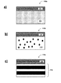
反射層系を備える積層体の形成中に基板に発生するこの機械的張力により、基板の曲率は、コーティング前の状態における元来の曲率から変化する。コーティング前の基板のこの元来の曲率は、ゼロ(すなわち、基板はコーティング前の平らな状態)、又は完成されたミラー素子の所望の意図される曲率に未だ対応していない最終曲率(例えば、凸状曲率)である。図5aによれば、例えば、同じ曲率又は屈折力を有する複数のミラー素子は、初期状態において平らな(ミラー)基板511,512・・・を、同じコーティングパラメータの設定された反射層系を備える積層体521,522・・・によってそれぞれコーティングすることによって製造することができ、このコーティング中、生成される機械的張力及びこの機械的張力によって生じるそれぞれの基板511,522・・・上の曲げ力は、(それぞれの場合において各ミラー素子と同一の)所望される曲率が各々の完成されたミラー素子において設定されるように選択される。図5bによれば、基板513,514・・・はそれぞれ初期状態(コーティング前)において最終曲率を有することもでき、この最終曲率は最終的に所望される曲率には未だ対応しておらず、この基板曲率は、積層体を適用する際に生成される機械的張力又はかけられる曲げ力によって変えられる。具体的には、図5bの例において、コーティング前の初期の状態で存在する基板513,514・・・の凸状曲率はゼロとなる、すなわち、完成したミラー素子の平らな幾何学的形状が最終的に生成される。
Due to this mechanical tension generated in the substrate during the formation of the laminate with the reflective layer system, the curvature of the substrate changes from the original curvature in the pre-coating state. This original curvature of the substrate before coating is zero (ie, the substrate is in a flat state before coating), or the final curvature that does not yet correspond to the desired intended curvature of the finished mirror element (eg, for example. Convex curvature). According to FIG. 5a, for example, a plurality of mirror elements having the same curvature or refractive power include a flat (mirror)
ここで本発明によるミラー素子の実施可能な実施形態を、図1のa)〜e)を参照して以下に説明する。実施形態において、本発明による「バイメタリック効果」の補償、すなわち、積層体によってかけられる、温度変化を伴う曲げ力のミラー素子の曲率への影響に関する変動の補償は、基板の構成を積層体の構成に、特にそれぞれに存在する平均熱膨張係数に関して適切に調整することによって実現される。 Here, a feasible embodiment of the mirror element according to the present invention will be described below with reference to a) to e) of FIG. In an embodiment, the compensation for the "bimetallic effect" according to the present invention, that is, the compensation for the influence of the bending force with temperature change on the curvature of the mirror element, which is applied by the laminate, is to make the structure of the substrate of the laminate. This is achieved by making appropriate adjustments to the configuration, especially with respect to the average coefficient of thermal expansion present in each.
具体的には、図1のa)〜e)によれば、ミラー素子110a〜110eの基板は、基板に使用される材料を考慮して、基板の平均熱膨張係数が、その値に関して、積層体の平均熱膨張係数にほぼ対応するように設計される(好適には、2つの値の内の大きい方に対して±3%以内)。
Specifically, according to a) to e) of FIG. 1, the substrates of the
一方の積層体と他方の基板との間の平均熱膨張係数の、基板の部分に対して求められる調整に関して適用される本発明による手段により、積層体又は反射層系の場合と異なる、材料の選択と設計が基板部分におけるミラー素子の所望される光学効果によって予め定められない状況は、基板部分が比較的大きな設計自由度を有するように利用される。 A material of a material that differs from the case of laminates or reflective layer systems by the means according to the invention applied with respect to the adjustment of the average coefficient of thermal expansion between one laminate and the other substrate for the portion of the substrate. Situations where selection and design are not predetermined by the desired optical effect of the mirror element on the substrate portion are utilized so that the substrate portion has a relatively large degree of design freedom.
図1のa)〜e)の各場合において略的に示すように、上述のような(図1のa)〜e)においてそれぞれ111,112,113,114及び115で示される)基板の(図1のa)〜e)においてそれぞれ121,122,123,124及び125で示される)積層体への適合は、基板(図1のa))の構成が均一の場合、基板材料は積層体の値にほぼ適合する適切な平均熱膨張係数をすでに有している、又は、基板部分のこの適合は、異なる熱膨張係数を有する別の材料のドーピング(図1のb))、若しくは別の材料の層(図1のc))又はカラム(図1のd))によって達成されるという事実によって実行することができる。図1のe)は更なる実施可能な実施形態の略図であり、この場合、基板115部分において、選択された種々の基板材料の混合物が複数の層に分布され、その結果、熱膨張係数の勾配が生じている。
As approximately shown in each of the cases a) to e) of FIG. 1, the substrate (indicated by 111, 112, 113, 114 and 115, respectively) in the above-mentioned (a) to e) of FIG. The compatibility with the laminate (shown by 121, 122, 123, 124 and 125 in a) to e) of FIG. 1 is that the substrate material is the laminate when the composition of the substrate (a in FIG. 1)) is uniform. Already has an appropriate average coefficient of thermal expansion that closely matches the value of, or this adaptation of the substrate portion is doping of another material with a different coefficient of thermal expansion (b in FIG. 1), or another. It can be carried out by the fact that it is achieved by a layer of material (c in FIG. 1)) or a column (d in FIG. 1). E) of FIG. 1 is a schematic representation of a further feasible embodiment, in which case in the
例えば、図1のb)において積層体122が5×10⁻⁶K−1の平均熱膨張係数を有する場合、基板112部分に存在する熱膨張係数の所望される対応は、シリコン(Si)とゲルマニウム(Ge)とで製造された合金として構成される基板によって達成することができる。シリコン(α=2.6×10⁻⁶K−1)とゲルマニウム(α=5.9×10⁻⁶K−1)の対応する熱膨張係数の値を考慮すると、この例示的実施形態に対して理想的なシリコン(Si)含有率は27%となる。第一次近似において、これは図1のc)及び図1のd)による例示的実施形態にも適用される。
For example, in b) of FIG. 1, when the laminate 122 has an average coefficient of thermal expansion of 5 × 10 -6 K- 1 , the desired correspondence of the coefficient of thermal expansion present in the
従って本発明は、上述の態様によれば、積層体の熱膨張係数が所定値の場合、基板の熱膨張係数を(「自由」パラメータとして)適切に選択することにより、結果として所望の補償効果を達成するという概念を含んでいる。 Therefore, according to the above aspect, when the coefficient of thermal expansion of the laminate is a predetermined value, the present invention results in a desired compensation effect by appropriately selecting the coefficient of thermal expansion of the substrate (as a "free" parameter). Includes the concept of achieving.
更に実施可能な実施形態を、図2〜図4を参照して以下に説明する。これらの実施形態において、本発明によるバイメタリック効果の補償は、基板又は基板材料の適切な適用によってのみでなく、一つ又は複数の追加層の使用によって達成される。 Further feasible embodiments will be described below with reference to FIGS. 2-4. In these embodiments, compensation for the bimetallic effect according to the invention is achieved not only by the proper application of the substrate or substrate material, but also by the use of one or more additional layers.
図2のa)〜c)によれば、基板は211,212又は213で示され、積層体(反射層系及び更なる機能層を任意に含む)は221,222又は223で示される。図2のa)〜図2のc)の例示的実施形態に共通していることは、各ミラー素子がそれぞれ補償層231,232又は233を有し、これは、温度変化を伴う、積層体221,222又は223によってかけられる曲げ力の変動を、それぞれのミラー素子210a,210b又は210cの曲率への影響に関して、少なくとも部分的に補償する働きをする。
According to FIGS. 2a)-c), the substrate is represented by 211,212 or 213, and the laminate (optionally including a reflective layer system and additional functional layers) is represented by 221,222 or 223. Common to the exemplary embodiments of FIGS. 2a) to 2c) is that each mirror element has a compensation layer 231,232 or 233, which is a laminate with temperature changes. It serves to at least partially compensate for the variation in bending force applied by 221,222 or 223 with respect to the effect on the curvature of the
図2のa)によれば、補償層231は基板211と積層体221の間に配置されている。この場合、補償層231は、例えば少なくとも10Kの温度間隔内の温度変化を伴う補償層231によってかけられる曲げ力の変動が、この温度変化によって熱的に誘導される積層体221の部分における曲げ力の変化と、強さに関して反対の符合で同等となるように構成される。換言すれば、以下の関係が当てはまる。

例えば、積層体221部分の平均熱膨張係数がα=5×10⁻⁶K−1、積層体221の厚さが500nmであり、基板が熱膨張係数α=2.6×10⁻⁶K−1のシリコン(Si)で製造されている場合、補償層231は熱膨張係数0.55×10⁻⁶K−1の二酸化ケイ素(SiO2)で製造することができ、この場合、補償層231の厚さは理想値585nmである。
For example, the average coefficient of thermal expansion of the
従って本態様によれば、本発明は、基板及び積層体の熱膨張係数α並びに積層体の厚さの所定値に基づき、補償層の対応するパラメータを適切に選択することによって、所望の補償効果を実現させるという概念を含んでいる。換言すれば、補償層の導入により、方程式(1)の所定のパラメータ、すなわちα基板、α積層体及びtf1を維持しつつ、(材料および厚さに関する)補償層の目標とする構成によって、所望の補償効果をより容易に達成することができる。 Therefore, according to the present invention, the present invention has a desired compensation effect by appropriately selecting the corresponding parameters of the compensation layer based on the predetermined values of the coefficient of thermal expansion α of the substrate and the laminate and the thickness of the laminate. Includes the concept of realizing. In other words, with the introduction of the compensating layer, by the target configuration of the compensating layer (with respect to material and thickness), while maintaining the predetermined parameters of equation (1), namely the α substrate , α laminate and t f1. The desired compensation effect can be achieved more easily.
図2のb)によれば、補償層232は積層体222と反対側の基板212の側面に配置することもできる。この場合、特定の温度間隔内で上述の温度変化によって熱的に誘導される補償層232の曲げ力は、好適には、積層体222によってかけられる曲げ力と、強さ及び符合に関して理想的に同等である。すなわち、以下の式が適用される:
図2のb)における基板212及び積層体222の構成の場合、これは、補償層232の理想的な厚さが59nmの場合、補償層232を熱膨張係数23×10−6K−1のアルミニウム(Al)で製造することによって達成することができる。
In the case of the configuration of the
図2のc)によれば、補償層233は更に、基板213の内部(すなわち、基板の上部でも下部でもない)にも配置させることができる。
According to c) of FIG. 2, the
図3のa)〜m)に略的に示す更なる実施形態において、更に張力誘導層を設けることができ、これは、所望の機械的張力又は所望の曲げ力が積層体によって基板にかけられるように構成されている。図3のa)〜m)において、基板はそれぞれ311a,311b・・・で示され、積層体はそれぞれ321a,321b・・・で示され、任意に追加されて存在する補償層はそれぞれ351b,351c・・・で示されている。 In a further embodiment substantially shown in FIGS. 3a) to 3m), a tension induction layer can be further provided so that the desired mechanical tension or desired bending force is applied to the substrate by the laminate. It is configured in. In FIGS. 3A) to 3M), the substrates are indicated by 311a, 311b ..., The laminates are indicated by 321a, 321b ..., respectively, and the compensation layers present by being arbitrarily added are 351b, respectively. It is indicated by 351c ....
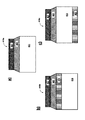
図3のa)、h)及びk)においては、全体に亘る機械的張力、又は積層体321a,321h若しくは321kによってかけられる曲げ力に対する調整は補償層331a,331h又は331kによって行われ、一方で残りの実施形態、すなわち、図3のb)〜g)、図3のi)〜j)及び図3のl)〜m)には追加の張力誘導層351b,351c・・・が設けられると仮定して、図2のa)〜c)に基づいて説明した上述の実施形態から生じる違いについて説明する。
In a), h) and k) of FIG. 3, the overall mechanical tension or the bending force applied by the
図4のa)は本発明の更なる実施形態を示す。本発明によるバイメタリック効果の補償は、均等層441の存在によって達成され、均等層は、(均等層441によって基板411と積層体421の間に機械的分離が生じるように)基板411と積層体421の間の機械的張力の伝達を低減させる。
A) of FIG. 4 shows a further embodiment of the present invention. Compensation for the bimetallic effect according to the present invention is achieved by the presence of the
図4のb)及び図4のc)は更なる例示的実施形態を示しており、これには、図3のa)〜m)と同様に、追加の張力誘導層452又は453が設けられている。
B) in FIG. 4 and c) in FIG. 4 show a further exemplary embodiment, which is provided with an additional
図6は、EUVでの動作用に設計された、本発明を実現させることのできる例示的投影露光装置の略図である。 FIG. 6 is a schematic representation of an exemplary projection exposure apparatus designed for EUV operation that can realize the present invention.
図6によれば、EUV用に設計された投影露光装置600内の照明デバイスは、視野ファセットミラー603及び瞳ファセットミラー604を備えている。プラズマ光源601及び集光ミラー602を備える光源部からの光は視野ファセットミラー603に向けられる。第1望遠鏡ミラー605及び第2望遠鏡ミラー606は瞳ファセットミラー604の下流の光路に配置されている。偏向ミラー607は光路の下流に配置され、これは、偏向ミラーに入射する光を、6つのミラー651〜656を含む投影レンズの物体平面の物体視野に向ける。物体視野にあるマスクステージ620には反射構造を有するマスク621が配置され、このマスクは投影レンズによって像面に結像され、ウエハステージ660上には感光層(フォトレジスト)でコーティングされた基板661がある。
According to FIG. 6, the illumination device in the
本発明はこれに限定されず、本発明による方法は、図6の視野ファセットミラー603又は瞳ファセットミラー604の製造に特に有利に適用することができ、更に、特に視野ファセットミラー603の各々の視野ファセット又は瞳ファセットミラー604の各々の瞳ファセットが各々のミラー素子又はマイクロミラーで構成されている場合、更に特に有利に適用することができる。
The present invention is not limited thereto, and the method according to the present invention can be applied particularly advantageously to the production of the
本発明を特定の実施形態に基づいて説明してきたが、例えば、各々の実施形態の特徴の組合せ及び/又は交換による多くの種々の代替実施形態が当業者には明らかであろう。従って、当業者にとって言うまでもないことだが、このような変形及び代替実施形態は本発明に付随して含まれ、本発明の範囲は、添付する特許請求項及びその同等物の範囲内のみに限定される。 Although the present invention has been described on the basis of specific embodiments, many different alternative embodiments by combining and / or exchanging the features of each embodiment will be apparent to those skilled in the art. Therefore, it goes without saying for those skilled in the art that such modifications and alternative embodiments are included in the invention and the scope of the invention is limited to the appended claims and their equivalents. To.
Claims (12)
‐基板(111,112,113,114,115,211,212,213,311a〜311m,411,412,413)と、
‐前記基板上の、少なくとも1つの反射層系を有する積層体(121,122,123,124,125,221,222,223,321a〜321m,421,422,423)とを備え、
‐前記ミラー素子の曲率は、所定の動作温度に対する所望の意図される曲率に基づいて、前記積層体によってかけられる非消失の曲げ力によって生成され、
‐前記生成された曲率は、少なくとも10Kの温度間隔(ΔT)に亘って10%以下で変動し、
前記ミラー素子は、補償層(231,232,233,331a,331b,・・・)を備え、該補償層は、前記温度間隔(ΔT)内で生じる温度変化を伴う、前記積層体(221,222,223,321a,321b・・・)によってかけられる曲げ力の変動を、該曲げ力の前記ミラー素子の曲率への影響に関して、少なくとも部分的に補償し、
前記ミラー素子は、所望の機械的張力又は所望の曲げ力が前記積層体によって前記基板にかけられるように構成された張力誘導層(351b,351c,・・・;452,453)を更に備え、該張力誘導層は、前記基板により前記補償層から分離されるミラー素子。 A mirror element,
-With the substrate (111,112,113,114,115,211,212,213,311a-311m, 411,421,413),
-With a laminate (121,122,123,124,125,221,222,223,321a to 321m, 421,422,423) having at least one reflective layer system on the substrate.
-The curvature of the mirror element is generated by the non-disappearing bending force applied by the laminate based on the desired intended curvature with respect to a given operating temperature.
-The generated curvature varies by less than 10% over a temperature interval (ΔT) of at least 10K.
The mirror element includes a compensating layer (231,232,233,331a, 331b, ...), The compensating layer includes the laminated body (221,) accompanied by a temperature change occurring within the temperature interval (ΔT). 222,223,321a, 321b ...), The variation of the bending force is compensated at least partially with respect to the influence of the bending force on the curvature of the mirror element .
The mirror element further comprises a tension induction layer (351b, 351c, ...; 452,453) configured such that a desired mechanical tension or a desired bending force is applied to the substrate by the laminate. The tension induction layer is a mirror element separated from the compensation layer by the substrate.
A microlithography projection exposure apparatus including an illumination device and a projection lens, the projection exposure apparatus including the optical system according to claim 11.
Applications Claiming Priority (2)
| Application Number | Priority Date | Filing Date | Title |
|---|---|---|---|
| DE102015225510.7 | 2015-12-16 | ||
| DE102015225510.7A DE102015225510A1 (en) | 2015-12-16 | 2015-12-16 | Mirror element, in particular for a microlithographic projection exposure apparatus |
Publications (3)
| Publication Number | Publication Date |
|---|---|
| JP2017126062A JP2017126062A (en) | 2017-07-20 |
| JP2017126062A5 JP2017126062A5 (en) | 2020-01-30 |
| JP6875846B2 true JP6875846B2 (en) | 2021-05-26 |
Family
ID=57584057
Family Applications (1)
| Application Number | Title | Priority Date | Filing Date |
|---|---|---|---|
| JP2016242654A Active JP6875846B2 (en) | 2015-12-16 | 2016-12-14 | Mirror elements especially for microlithography projection exposure equipment |
Country Status (3)
| Country | Link |
|---|---|
| US (2) | US20170176741A1 (en) |
| JP (1) | JP6875846B2 (en) |
| DE (1) | DE102015225510A1 (en) |
Families Citing this family (1)
| Publication number | Priority date | Publication date | Assignee | Title |
|---|---|---|---|---|
| US20200201027A1 (en) * | 2018-12-21 | 2020-06-25 | Didi Research America, Llc | Micromachined mirror assembly having multiple coating layers |
Family Cites Families (18)
| Publication number | Priority date | Publication date | Assignee | Title |
|---|---|---|---|---|
| DE10314212B4 (en) | 2002-03-29 | 2010-06-02 | Hoya Corp. | Method for producing a mask blank, method for producing a transfer mask |
| US6994444B2 (en) | 2002-06-14 | 2006-02-07 | Asml Holding N.V. | Method and apparatus for managing actinic intensity transients in a lithography mirror |
| US6778315B2 (en) * | 2002-09-25 | 2004-08-17 | Rosemount Aerospace Inc. | Micro mirror structure with flat reflective coating |
| EP1668421A2 (en) | 2003-09-12 | 2006-06-14 | Carl Zeiss SMT AG | Illumination system for a microlithography projection exposure installation |
| JP2007108194A (en) * | 2005-10-11 | 2007-04-26 | Canon Inc | Method for manufacturing multilayer film mirror, method for manufacturing optical system, exposure device, and method for manufacturing device |
| EP1945829A1 (en) | 2005-11-10 | 2008-07-23 | Asahi Glass Company, Limited | Method for depositing reflective multilayer film of reflective mask blank for euv lithography and method for producing reflective mask blank for euv lithography |
| US7261430B1 (en) * | 2006-02-22 | 2007-08-28 | Teledyne Licensing, Llc | Thermal and intrinsic stress compensated micromirror apparatus and method |
| DE102006057567B4 (en) | 2006-11-28 | 2008-09-04 | Micronic Laser Systems Ab | Microoptical element with a substrate on which at least one height level is formed on an optically active surface, process for its preparation and uses |
| DE102006057568A1 (en) * | 2006-11-28 | 2008-05-29 | Micronic Laser Systems Ab | Microoptical element with a substrate and method for its production |
| DE102008009600A1 (en) | 2008-02-15 | 2009-08-20 | Carl Zeiss Smt Ag | Facet mirror e.g. field facet mirror, for use as bundle-guiding optical component in illumination optics of projection exposure apparatus, has single mirror tiltable by actuators, where object field sections are smaller than object field |
| CN103293665B (en) * | 2008-02-15 | 2016-07-06 | 卡尔蔡司Smt有限责任公司 | The facet mirror that the projection exposure apparatus of micro-lithography uses |
| DE102008042212A1 (en) | 2008-09-19 | 2010-04-01 | Carl Zeiss Smt Ag | Reflective optical element and method for its production |
| JP5549222B2 (en) * | 2009-12-28 | 2014-07-16 | 株式会社ニコン | Spatial light modulator, exposure apparatus and manufacturing method thereof |
| DE102010028488A1 (en) | 2010-05-03 | 2011-11-03 | Carl Zeiss Smt Gmbh | Substrates for mirrors for EUV lithography and their preparation |
| DE102010017106A1 (en) * | 2010-05-27 | 2011-12-01 | Carl Zeiss Laser Optics Gmbh | Mirror with dielectric coating |
| DE102011003357A1 (en) | 2011-01-31 | 2012-08-02 | Carl Zeiss Smt Gmbh | Mirror for the EUV wavelength range, production method for such a mirror, projection objective for microlithography with such a mirror and microlithography projection exposure apparatus with such a projection objective |
| DE102014201622A1 (en) | 2014-01-30 | 2015-08-20 | Carl Zeiss Smt Gmbh | Method for producing a mirror element |
| DE102015200328A1 (en) | 2015-01-13 | 2016-07-14 | Carl Zeiss Smt Gmbh | Method for producing an optical element for an optical system, in particular for a coprolithographic projection exposure apparatus |
-
2015
- 2015-12-16 DE DE102015225510.7A patent/DE102015225510A1/en not_active Ceased
-
2016
- 2016-12-14 JP JP2016242654A patent/JP6875846B2/en active Active
- 2016-12-16 US US15/381,910 patent/US20170176741A1/en not_active Abandoned
-
2017
- 2017-12-11 US US15/837,932 patent/US10598921B2/en active Active
Also Published As
| Publication number | Publication date |
|---|---|
| US20180101002A1 (en) | 2018-04-12 |
| DE102015225510A1 (en) | 2017-01-12 |
| US10598921B2 (en) | 2020-03-24 |
| US20170176741A1 (en) | 2017-06-22 |
| JP2017126062A (en) | 2017-07-20 |
Similar Documents
| Publication | Publication Date | Title |
|---|---|---|
| JP6550066B2 (en) | Method of manufacturing a mirror element | |
| US9798254B2 (en) | Arrangement for the thermal actuation of a mirror, in particular in a microlithographic projection exposure apparatus | |
| JP5487110B2 (en) | Microlithography projection exposure apparatus | |
| US9785054B2 (en) | Mirror, more particularly for a microlithographic projection exposure apparatus | |
| KR101288782B1 (en) | Optical element for uv or euv lithography | |
| JP2002520601A (en) | Mirror substrate coated with SiO2 for EUV | |
| TW201022854A (en) | Illumination system of a microlithographic projection exposure apparatus | |
| JP6399889B2 (en) | Reflective optical element | |
| US11187990B2 (en) | Mirror for a microlithographic projection exposure apparatus, and method for operating a deformable mirror | |
| TWI684069B (en) | Optical arrangement of a microlithographic projection exposure apparatus | |
| JP2010533370A (en) | Optical system for microlithographic projection exposure apparatus | |
| US20170315452A1 (en) | Method For Producing An Optical Element For An Optical System, In Particular For A Microlithographic Projection Exposure Apparatus | |
| US10151922B2 (en) | Wavefront correction element for use in an optical system | |
| JP6875846B2 (en) | Mirror elements especially for microlithography projection exposure equipment | |
| TW202328826A (en) | Optical element for the beam guidance of imaging light in projection lithography | |
| CN114072731A (en) | Method and device for producing an adhesive bond between a first component and a second component | |
| KR20210035181A (en) | Method and device for determining the heating state of an optical element in an optical system for microlithography | |
| US7522260B1 (en) | Method for correcting astigmatism in a microlithography projection exposure apparatus, a projection objective of such a projection exposure apparatus, and a fabrication method for micropatterned components | |
| TW202210953A (en) | Mirror, in particular for a microlithographic projection exposure apparatus | |
| JP6862154B2 (en) | Manufacturing methods for optics, exposure equipment, and articles | |
| JP2024507881A (en) | Optical assembly, method for deforming optical elements, and projection exposure system | |
| JP2023530521A (en) | Mirrors, especially in microlithographic projection exposure systems | |
| KR20200106903A (en) | Optical element for beam guidance of imaging light in projection lithography |
Legal Events
| Date | Code | Title | Description |
|---|---|---|---|
| A521 | Request for written amendment filed |
Free format text: JAPANESE INTERMEDIATE CODE: A523 Effective date: 20191212 |
|
| A621 | Written request for application examination |
Free format text: JAPANESE INTERMEDIATE CODE: A621 Effective date: 20191212 |
|
| A977 | Report on retrieval |
Free format text: JAPANESE INTERMEDIATE CODE: A971007 Effective date: 20201009 |
|
| A131 | Notification of reasons for refusal |
Free format text: JAPANESE INTERMEDIATE CODE: A131 Effective date: 20201020 |
|
| A521 | Request for written amendment filed |
Free format text: JAPANESE INTERMEDIATE CODE: A523 Effective date: 20201221 |
|
| TRDD | Decision of grant or rejection written | ||
| A01 | Written decision to grant a patent or to grant a registration (utility model) |
Free format text: JAPANESE INTERMEDIATE CODE: A01 Effective date: 20210413 |
|
| A61 | First payment of annual fees (during grant procedure) |
Free format text: JAPANESE INTERMEDIATE CODE: A61 Effective date: 20210423 |
|
| R150 | Certificate of patent or registration of utility model |
Ref document number: 6875846 Country of ref document: JP Free format text: JAPANESE INTERMEDIATE CODE Ref document number: 6875846 Country of ref document: JP Free format text: JAPANESE INTERMEDIATE CODE: R150 |
|
| R250 | Receipt of annual fees |
Free format text: JAPANESE INTERMEDIATE CODE: R250 |