JP6861602B2 - Holding member, manufacturing method of holding member, holding mechanism and product manufacturing equipment - Google Patents
Holding member, manufacturing method of holding member, holding mechanism and product manufacturing equipment Download PDFInfo
- Publication number
- JP6861602B2 JP6861602B2 JP2017177223A JP2017177223A JP6861602B2 JP 6861602 B2 JP6861602 B2 JP 6861602B2 JP 2017177223 A JP2017177223 A JP 2017177223A JP 2017177223 A JP2017177223 A JP 2017177223A JP 6861602 B2 JP6861602 B2 JP 6861602B2
- Authority
- JP
- Japan
- Prior art keywords
- holding member
- product
- bga
- cured resin
- held
- Prior art date
- Legal status (The legal status is an assumption and is not a legal conclusion. Google has not performed a legal analysis and makes no representation as to the accuracy of the status listed.)
- Active
Links
- 238000004519 manufacturing process Methods 0.000 title claims description 50
- 230000007246 mechanism Effects 0.000 title claims description 17
- 229920005989 resin Polymers 0.000 claims description 184
- 239000011347 resin Substances 0.000 claims description 184
- 238000005520 cutting process Methods 0.000 claims description 102
- 239000000463 material Substances 0.000 claims description 50
- 238000000465 moulding Methods 0.000 claims description 46
- 238000000034 method Methods 0.000 claims description 30
- 230000008569 process Effects 0.000 claims description 18
- 230000000717 retained effect Effects 0.000 claims description 7
- 230000000149 penetrating effect Effects 0.000 claims description 5
- 238000003825 pressing Methods 0.000 claims description 4
- 239000000758 substrate Substances 0.000 description 106
- 239000000047 product Substances 0.000 description 88
- 230000007723 transport mechanism Effects 0.000 description 22
- 238000007689 inspection Methods 0.000 description 20
- 238000003860 storage Methods 0.000 description 20
- 238000007789 sealing Methods 0.000 description 17
- 230000002093 peripheral effect Effects 0.000 description 15
- 230000004048 modification Effects 0.000 description 13
- 238000012986 modification Methods 0.000 description 13
- 229910000679 solder Inorganic materials 0.000 description 11
- 230000003287 optical effect Effects 0.000 description 9
- 238000003754 machining Methods 0.000 description 8
- 230000003014 reinforcing effect Effects 0.000 description 8
- 230000002950 deficient Effects 0.000 description 7
- 230000000694 effects Effects 0.000 description 7
- 239000013067 intermediate product Substances 0.000 description 6
- 229910052751 metal Inorganic materials 0.000 description 6
- 239000002184 metal Substances 0.000 description 6
- 230000032258 transport Effects 0.000 description 6
- 238000012545 processing Methods 0.000 description 5
- 239000004065 semiconductor Substances 0.000 description 5
- 230000009471 action Effects 0.000 description 4
- 230000006837 decompression Effects 0.000 description 4
- XLYOFNOQVPJJNP-UHFFFAOYSA-N water Substances O XLYOFNOQVPJJNP-UHFFFAOYSA-N 0.000 description 4
- XUIMIQQOPSSXEZ-UHFFFAOYSA-N Silicon Chemical compound [Si] XUIMIQQOPSSXEZ-UHFFFAOYSA-N 0.000 description 3
- 238000013459 approach Methods 0.000 description 3
- 239000012467 final product Substances 0.000 description 3
- 239000011521 glass Substances 0.000 description 3
- 238000001746 injection moulding Methods 0.000 description 3
- 229910052710 silicon Inorganic materials 0.000 description 3
- 239000010703 silicon Substances 0.000 description 3
- 239000002131 composite material Substances 0.000 description 2
- 239000000498 cooling water Substances 0.000 description 2
- 238000000280 densification Methods 0.000 description 2
- 239000007788 liquid Substances 0.000 description 2
- 239000012779 reinforcing material Substances 0.000 description 2
- 238000001179 sorption measurement Methods 0.000 description 2
- 238000012546 transfer Methods 0.000 description 2
- RYGMFSIKBFXOCR-UHFFFAOYSA-N Copper Chemical compound [Cu] RYGMFSIKBFXOCR-UHFFFAOYSA-N 0.000 description 1
- 239000004593 Epoxy Substances 0.000 description 1
- NIXOWILDQLNWCW-UHFFFAOYSA-N acrylic acid group Chemical group C(C=C)(=O)O NIXOWILDQLNWCW-UHFFFAOYSA-N 0.000 description 1
- 230000001154 acute effect Effects 0.000 description 1
- 239000000853 adhesive Substances 0.000 description 1
- 230000001070 adhesive effect Effects 0.000 description 1
- 229910052782 aluminium Inorganic materials 0.000 description 1
- XAGFODPZIPBFFR-UHFFFAOYSA-N aluminium Chemical compound [Al] XAGFODPZIPBFFR-UHFFFAOYSA-N 0.000 description 1
- 238000003491 array Methods 0.000 description 1
- 230000008901 benefit Effects 0.000 description 1
- 230000015572 biosynthetic process Effects 0.000 description 1
- 239000000919 ceramic Substances 0.000 description 1
- 238000004140 cleaning Methods 0.000 description 1
- 239000011889 copper foil Substances 0.000 description 1
- 239000002994 raw material Substances 0.000 description 1
- 230000003252 repetitive effect Effects 0.000 description 1
- 229920002050 silicone resin Polymers 0.000 description 1
Images


Classifications
-
- H—ELECTRICITY
- H01—ELECTRIC ELEMENTS
- H01L—SEMICONDUCTOR DEVICES NOT COVERED BY CLASS H10
- H01L21/00—Processes or apparatus adapted for the manufacture or treatment of semiconductor or solid state devices or of parts thereof
- H01L21/02—Manufacture or treatment of semiconductor devices or of parts thereof
- H01L21/04—Manufacture or treatment of semiconductor devices or of parts thereof the devices having at least one potential-jump barrier or surface barrier, e.g. PN junction, depletion layer or carrier concentration layer
- H01L21/50—Assembly of semiconductor devices using processes or apparatus not provided for in a single one of the subgroups H01L21/06 - H01L21/326, e.g. sealing of a cap to a base of a container
- H01L21/56—Encapsulations, e.g. encapsulation layers, coatings
- H01L21/565—Moulds
-
- B—PERFORMING OPERATIONS; TRANSPORTING
- B29—WORKING OF PLASTICS; WORKING OF SUBSTANCES IN A PLASTIC STATE IN GENERAL
- B29C—SHAPING OR JOINING OF PLASTICS; SHAPING OF MATERIAL IN A PLASTIC STATE, NOT OTHERWISE PROVIDED FOR; AFTER-TREATMENT OF THE SHAPED PRODUCTS, e.g. REPAIRING
- B29C43/00—Compression moulding, i.e. applying external pressure to flow the moulding material; Apparatus therefor
- B29C43/02—Compression moulding, i.e. applying external pressure to flow the moulding material; Apparatus therefor of articles of definite length, i.e. discrete articles
- B29C43/021—Compression moulding, i.e. applying external pressure to flow the moulding material; Apparatus therefor of articles of definite length, i.e. discrete articles characterised by the shape of the surface
-
- B—PERFORMING OPERATIONS; TRANSPORTING
- B29—WORKING OF PLASTICS; WORKING OF SUBSTANCES IN A PLASTIC STATE IN GENERAL
- B29C—SHAPING OR JOINING OF PLASTICS; SHAPING OF MATERIAL IN A PLASTIC STATE, NOT OTHERWISE PROVIDED FOR; AFTER-TREATMENT OF THE SHAPED PRODUCTS, e.g. REPAIRING
- B29C33/00—Moulds or cores; Details thereof or accessories therefor
- B29C33/42—Moulds or cores; Details thereof or accessories therefor characterised by the shape of the moulding surface, e.g. ribs or grooves
-
- B—PERFORMING OPERATIONS; TRANSPORTING
- B29—WORKING OF PLASTICS; WORKING OF SUBSTANCES IN A PLASTIC STATE IN GENERAL
- B29C—SHAPING OR JOINING OF PLASTICS; SHAPING OF MATERIAL IN A PLASTIC STATE, NOT OTHERWISE PROVIDED FOR; AFTER-TREATMENT OF THE SHAPED PRODUCTS, e.g. REPAIRING
- B29C43/00—Compression moulding, i.e. applying external pressure to flow the moulding material; Apparatus therefor
- B29C43/32—Component parts, details or accessories; Auxiliary operations
- B29C43/36—Moulds for making articles of definite length, i.e. discrete articles
-
- H—ELECTRICITY
- H01—ELECTRIC ELEMENTS
- H01L—SEMICONDUCTOR DEVICES NOT COVERED BY CLASS H10
- H01L23/00—Details of semiconductor or other solid state devices
- H01L23/02—Containers; Seals
- H01L23/04—Containers; Seals characterised by the shape of the container or parts, e.g. caps, walls
- H01L23/053—Containers; Seals characterised by the shape of the container or parts, e.g. caps, walls the container being a hollow construction and having an insulating or insulated base as a mounting for the semiconductor body
-
- H—ELECTRICITY
- H01—ELECTRIC ELEMENTS
- H01L—SEMICONDUCTOR DEVICES NOT COVERED BY CLASS H10
- H01L23/00—Details of semiconductor or other solid state devices
- H01L23/12—Mountings, e.g. non-detachable insulating substrates
- H01L23/13—Mountings, e.g. non-detachable insulating substrates characterised by the shape
-
- H—ELECTRICITY
- H01—ELECTRIC ELEMENTS
- H01L—SEMICONDUCTOR DEVICES NOT COVERED BY CLASS H10
- H01L33/00—Semiconductor devices with at least one potential-jump barrier or surface barrier specially adapted for light emission; Processes or apparatus specially adapted for the manufacture or treatment thereof or of parts thereof; Details thereof
- H01L33/48—Semiconductor devices with at least one potential-jump barrier or surface barrier specially adapted for light emission; Processes or apparatus specially adapted for the manufacture or treatment thereof or of parts thereof; Details thereof characterised by the semiconductor body packages
- H01L33/52—Encapsulations
- H01L33/54—Encapsulations having a particular shape
-
- H—ELECTRICITY
- H01—ELECTRIC ELEMENTS
- H01L—SEMICONDUCTOR DEVICES NOT COVERED BY CLASS H10
- H01L2933/00—Details relating to devices covered by the group H01L33/00 but not provided for in its subgroups
- H01L2933/0008—Processes
- H01L2933/0033—Processes relating to semiconductor body packages
- H01L2933/005—Processes relating to semiconductor body packages relating to encapsulations
Description
本発明は、製品を保持する保持部材、保持部材の製造方法、保持機構及び製品の製造装置に関する。 The present invention relates to a holding member for holding a product, a method for manufacturing the holding member, a holding mechanism, and a product manufacturing apparatus.
製品である保持対象品を保持する際に使用される保持部材として、トレイ(tray)等が挙げられる。貫通穴からなる吸着穴を経由して保持対象品を吸引することによって、保持部材が有する面に保持対象品を一時的に密着させて固定する(吸着する)場合がある。この場合に使用される吸着穴を有する吸着ジグ等も保持部材に含まれる。保持部材に設けられた吸引孔を使用して保持対象品を吸引することによって、保持対象品が保持部材の面に吸着される。吸着とは、大気圧によって保持対象品が保持部材の面に対して押圧されることによって、保持対象品が保持部材の面に密着することをいう。 Examples of the holding member used when holding the product to be held include a tray and the like. By sucking the product to be held through the suction hole formed of the through hole, the product to be held may be temporarily brought into close contact with the surface of the holding member and fixed (sucked). A suction jig or the like having a suction hole used in this case is also included in the holding member. By sucking the product to be held using the suction holes provided in the holding member, the product to be held is attracted to the surface of the holding member. Adsorption means that the product to be held is pressed against the surface of the holding member by atmospheric pressure, so that the product to be held is brought into close contact with the surface of the holding member.
製品である保持対象品の好適な例として、半導体集積回路(semiconductor integrated circuit;ICと略称する)であるICパッケージが挙げられる。ICパッケージは、回転刃を使用して封止済基板を切断して個片化すること(singulation )によって製造される。ICパッケージは最終製品であり、封止済基板は中間製品である。個片化される直前の封止済基板自体が取り引きされる場合があるので、封止済基板も製品に含まれる。 A suitable example of a product to be retained is an IC package which is a semiconductor integrated circuit (abbreviated as IC). IC packages are manufactured by cutting and singulating a sealed substrate using a rotary blade. The IC package is the final product and the sealed substrate is the intermediate product. Since the sealed substrate itself immediately before being separated into pieces may be traded, the sealed substrate is also included in the product.
封止済基板は、基板と、半導体チップ等を含むチップ(chip)と、硬化樹脂からなる封止樹脂とを含む、複合部材である。基板は、リードフレーム(lead frame)、プリント基板(printed wiring board )、セラミックス基板(ceramics substrate )、半導体基板(semiconductor wafer )等を含む。半導体基板は、シリコン基板(silicon wafer )、SiC 基板(SiC wafer )等を含む。基板は、論理回路、記憶回路、増幅回路等を含む電気回路が形成された回路基板と、チップを支持するための支持用基板とを含む。支持用基板は支持体(carrier )であって、シリコン基板、ガラス基板等を含む。 The sealed substrate is a composite member including the substrate, a chip containing a semiconductor chip and the like, and a sealing resin made of a cured resin. The substrate includes a lead frame, a printed wiring board, a ceramics substrate, a semiconductor wafer, and the like. The semiconductor substrate includes a silicon substrate (silicon wafer), a SiC substrate (SiC wafer), and the like. The substrate includes a circuit board on which an electric circuit including a logic circuit, a storage circuit, an amplifier circuit, and the like is formed, and a support substrate for supporting the chip. The supporting substrate is a carrier and includes a silicon substrate, a glass substrate, and the like.
保持部材の一種として、射出成形法を使用して樹脂成形することによって製造されるIC用トレイが提案されている(特許文献1の第4頁左上欄、第1図を参照)。このIC用トレイは、縦横直交する格子で仕切られている。1つの格子当たりに1つの半導体集積回路装置が積載されるQFP(quad flat package)型IC用トレイが、成形型を使用する射出成形法によって作成される。QFP 型ICはICパッケージに相当する。成形型は、機械加工、放電加工等によって製作される。
As a kind of holding member, an IC tray manufactured by resin molding using an injection molding method has been proposed (see FIG. 1 in the upper left column of
近年、ICパッケージ及び封止済基板を含む製品の形状、構成、1枚の封止済基板から製造されるICパッケージの数(取れ数)等が多様化している。取れ数としては、1枚の封止済基板から1,000 個単位(例えば、3,000〜5,000個)の製品が製造される場合が現れてきた。ICパッケージの一種として、個片化された回路基板においてはんだボールが格子状に形成された、ボールグリッドアレイ(ball grid array:BGA)パッケージ(以下「BGA パッケージ」という。)と呼ばれるタイプが存在する。 In recent years, the shapes and configurations of products including IC packages and sealed substrates have been diversified, such as the number of IC packages manufactured from one sealed substrate. As for the number of products to be taken, there have been cases where 1,000 pieces (for example, 3,000 to 5,000 pieces) of products are manufactured from one sealed substrate. As a type of IC package, there is a type called a ball grid array (BGA) package (hereinafter referred to as "BGA package") in which solder balls are formed in a grid pattern on an individualized circuit board. ..
BGA が有するはんだボールは、例えば、0.1〜1.0mm程度の直径を有する凸部である。BGA を製造する際の封止済基板(以下「BGA 用封止済基板」という。)は、回路基板に形成された多数のはんだボールを有する。BGA 用封止済基板が個片化されることによって製造された個々のBGA も、回路基板に形成された多数のはんだボールを有する。BGA 用封止済基板及びBGA を吸着する場合には、多数の凸部である多数のはんだボールの頂部と、回路基板の面(凸部である多数のはんだボールに対する凹部の底面)との間において、隙間が生じやすい。その隙間を通って空気が流動するので、BGA 用封止済基板及びBGA 自体を吸着する吸着力が弱くなる。したがって、個片化工程、搬送工程等において、BGA 用封止済基板及びBGA 自体が、吸着機能を有する保持部材において意図に反して移動するという不具合が発生するおそれがある。 The solder ball of the BGA is, for example, a convex portion having a diameter of about 0.1 to 1.0 mm. A sealed substrate for manufacturing a BGA (hereinafter referred to as "sealed substrate for BGA") has a large number of solder balls formed on a circuit board. Each BGA manufactured by disassembling the sealed substrate for BGA also has a large number of solder balls formed on the circuit board. When the sealed substrate for BGA and BGA are adsorbed, between the tops of many solder balls, which are many protrusions, and the surface of the circuit board (the bottom surface of the recesses for many solder balls, which are convex parts). In, a gap is likely to occur. Since air flows through the gap, the adsorption force for adsorbing the sealed substrate for BGA and the BGA itself is weakened. Therefore, in the individualization process, the transfer process, etc., there is a possibility that the sealed substrate for BGA and the BGA itself may move unintentionally in the holding member having a suction function.
BGA 用封止済基板及びBGA を、吸着機能を有する保持部材に十分に吸着させるため構成として、1個の製品が有する複数のはんだボールがすべて収容される凹部を、取れ数に等しい数だけ有する保持部材を形成するという構成が挙げられる。この場合においては、射出成形用の成形型における保持対象品の配置面に対応する面に、取れ数に等しい数の凹部に対応する凸部を形成する必要がある。機械加工、放電加工等によって1,000 個単位の凸部を成形型に形成することは、成形型の製造コストを増大させるという問題を生む。同様に、吸着機能を有さない保持部材(例えば、トレイ)を成形型を使用して製造する場合においても、成形型の製造コストを増大させるという問題が生じる。 As a configuration for sufficiently adsorbing the sealed substrate for BGA and the BGA to the holding member having a suction function, there are as many recesses as the number of recesses in which a plurality of solder balls of one product are accommodated. An example is a configuration in which a holding member is formed. In this case, it is necessary to form convex portions corresponding to the number of concave portions equal to the number of taken parts on the surface corresponding to the arrangement surface of the product to be held in the molding mold for injection molding. Forming 1,000 convex parts in a molding die by machining, electric discharge machining, etc. causes a problem of increasing the manufacturing cost of the molding die. Similarly, when a holding member (for example, a tray) having no suction function is manufactured by using a molding die, there arises a problem of increasing the manufacturing cost of the molding die.
本発明は、上述した問題を解決するためになされた。本発明は、凹凸を有する保持対象品を保持する際に使用される保持部材を安価に製造することを目的とする。 The present invention has been made to solve the above-mentioned problems. An object of the present invention is to inexpensively manufacture a holding member used for holding a holding object having irregularities.
上記の課題を解決するために、本発明に係る保持部材の製造方法は、保持対象品が保持される保持部材を製造する保持部材の製造方法であって、第1の幅を有する複数の溝部を主面に有する成形型を準備する工程と、成形型を樹脂材料に対向して配置する工程と、成形型の主面を樹脂材料に押し付ける工程と、樹脂材料を硬化させて硬化樹脂を形成することによって硬化樹脂を含む成形品を成形する工程と、成形型から成形品を取り外す工程とを備え、成形品は、複数の溝部が硬化樹脂に転写されることによって形成された複数の壁部と、複数の壁部に取り囲まれた凹部とを備えた保持部材であり、硬化樹脂の外底面から硬化樹脂の内底面を見た場合に保持対象品が凹部を包含するようにして保持対象品が保持される。 In order to solve the above problems, the method for manufacturing a holding member according to the present invention is a method for manufacturing a holding member for manufacturing a holding member for holding an object to be held, and is a method for manufacturing a holding member having a first width. A step of preparing a molding die having a main surface, a step of arranging the molding die facing the resin material, a step of pressing the main surface of the molding die against the resin material, and a step of curing the resin material to form a cured resin. The molded product includes a step of molding a molded product containing a cured resin and a step of removing the molded product from the molding mold, and the molded product has a plurality of wall portions formed by transferring a plurality of grooves to the cured resin. It is a holding member provided with a recess surrounded by a plurality of wall portions, and when the inner bottom surface of the cured resin is viewed from the outer bottom surface of the cured resin, the retained object product includes the recessed portion. Is retained.
上記の課題を解決するために、本発明に係る保持部材は、保持対象品が保持される保持部材であって、樹脂材料が硬化して形成され、保持対象品に接する接触面を有する硬化樹脂と、硬化樹脂に含まれ、第1の方向に沿って伸びる複数の第1の壁部と、硬化樹脂に含まれ、第1の方向と交わる第2の方向に沿って伸びる複数の第2の壁部と、複数の第1の壁部と複数の第2の壁部とによって取り囲まれた凹部とを備え、硬化樹脂の外底面から硬化樹脂の内底面を見た場合に保持対象品が凹部を包含するようにして保持対象品が保持され、複数の第1の壁部が有する形状は、成形型の主面において形成され第1の幅を有する複数の第1の溝部の形状が硬化樹脂に転写された形状であり、複数の第2の壁部が有する形状は、成形型の主面において形成され第1の幅を有する複数の第2の溝部の形状が硬化樹脂に転写された形状である。 In order to solve the above problems, the holding member according to the present invention is a holding member for holding the holding target product, and is a cured resin formed by curing the resin material and having a contact surface in contact with the holding target product. And a plurality of first wall portions contained in the cured resin and extending along the first direction, and a plurality of second walls contained in the cured resin and extending along the second direction intersecting the first direction. It is provided with a wall portion and a recess surrounded by a plurality of first wall portions and a plurality of second wall portions, and when the inner bottom surface of the cured resin is viewed from the outer bottom surface of the cured resin, the product to be held is recessed. The object to be held is held so as to include the above, and the shape of the plurality of first wall portions is such that the shape of the plurality of first grooves having the first width formed on the main surface of the molding mold is a cured resin. The shape of the plurality of second wall portions is the shape transferred to the cured resin, and the shape of the plurality of second groove portions having the first width formed on the main surface of the molding die is transferred to the cured resin. Is.
上記の課題を解決するために、本発明に係る保持機構は、上述した保持部材を有する。 In order to solve the above problems, the holding mechanism according to the present invention has the above-mentioned holding member.
上記の課題を解決するために、本発明に係る製品の製造装置は、上述した保持部材を有する。 In order to solve the above problems, the product manufacturing apparatus according to the present invention has the above-mentioned holding member.
本発明によれば、製造コストを増大させることなく保持部材を製造することができる。 According to the present invention, the holding member can be manufactured without increasing the manufacturing cost.
以下、本発明に係る実施形態について、図面を参照して説明する。本出願書類におけるいずれの図についても、わかりやすくするために、適宜省略し又は誇張して模式的に描かれている。同一の構成要素については、同一の符号を付して説明を適宜省略する。 Hereinafter, embodiments according to the present invention will be described with reference to the drawings. All figures in the application documents are schematically drawn with omission or exaggeration for the sake of clarity. The same components are designated by the same reference numerals and the description thereof will be omitted as appropriate.
〔実施形態1〕
(BGA 用封止済基板の構成)
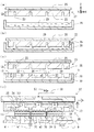
図1を参照して、BGA 用封止済基板の構成を説明する。BGA 用封止済基板を切断することによって、最終製品であるBGA パッケージが製造される。したがって、BGA 用封止済基板は、BGA パッケージを製造する際の中間製品に相当する。最終製品に相当するBGA パッケージは、保持部材に保持される保持対象品である。
[Embodiment 1]
(Structure of sealed substrate for BGA)
The configuration of the sealed substrate for BGA will be described with reference to FIG. The final product, the BGA package, is manufactured by cutting the sealed substrate for BGA. Therefore, the sealed substrate for BGA corresponds to an intermediate product in manufacturing a BGA package. The BGA package, which corresponds to the final product, is the product to be held that is held by the holding member.
図1(b)に示されるように、BGA 用封止済基板1が備える基板2は、複数の領域3を有する。基板2の一方の面2aにおいて、各領域3にはチップ4がそれぞれ装着される。基板2の一方の面2aには、複数の領域3におけるチップ4が覆われるようにして、封止樹脂5が成形される。各チップ4は、封止樹脂5によって一括して樹脂封止される。BGA 用封止済基板1は、基板2とチップ4と封止樹脂5とを備える。
As shown in FIG. 1 (b), the
図1に示されるように、BGA 用封止済基板1の他方の面2bには多数の突起状電極6が設けられる。突起状電極6は、BGA 用封止済基板1の他方の面2bから突出する凸部である。突起状電極6が他方の面2bから突出する長さである突出量は、距離Laである。突起状電極6は、BGA パッケージとBGA パッケージの外部とを電気的に接続する外部端子として機能する。図1には、突起状電極6としてはんだボールが示される。図1は、BGA 用封止済基板1が有する1個の領域3全体に突起状電極6が設けられる場合を示す。BGA 用封止済基板1の他方の面2bにおいて、突起状電極6は凸部であり、突起状電極6以外の部分(言い換えると、他方の面2bにおける突起状電極6以外の部分)は凹部である。
As shown in FIG. 1, a large number of
図1(a)に示されるように、BGA 用封止済基板1には、X方向に沿って伸びる複数の第1切断線7とY方向に沿って伸びる複数の第2切断線8とが、それぞれ仮想的に設定される。複数の第1切断線7と複数の第2切断線8とによって囲まれる複数の領域3が、それぞれ保持対象品であるBGA パッケージに相当する。図1(a)に示される領域3の平面形状(Z方向に沿って見た形状。以下同じ。)は、一辺の長さaである4つの辺を有する正方形である。
As shown in FIG. 1A, the sealed
図1(a)においては、X方向に沿って3個の領域3が形成され、Y方向に沿って4個の領域3が形成される。したがって、BGA 用封止済基板1に12個の領域3が格子状に形成される。複数の第1切断線7と複数の第2切断線8とに沿ってBGA 用封止済基板1が切断されることによって、それぞれの領域3に相当する12個のBGA パッケージが製造される。BGA 用封止済基板1の大きさは、個片化されるBGA パッケージのサイズや取れ数に応じて任意に設定される。
In FIG. 1A, three
(BGA パッケージの製造方法)
図2(a)を参照して、BGA 用封止済基板1からBGA パッケージを製造する方法を説明する。まず、切断テーブル9を準備する。切断テーブル9には、切断用ジグ10が取り付けられる。切断用ジグ10は、金属プレート11と金属プレート11の上に取り付けられた樹脂シート12とを有する。切断テーブル9の上面に金属プレート11が取り付けられる。樹脂シート12の上面には、BGA 用封止済基板1が有する複数の第1切断線7(図1参照)と複数の第2切断線8とに重なるようにして、切断溝13が形成される。
(Manufacturing method of BGA package)
A method of manufacturing a BGA package from the sealed
切断用ジグ10は、金属プレート11と樹脂シート12とを貫通する貫通穴14を有する。貫通穴14は、BGA 用封止済基板1が有する領域3にそれぞれ対応して形成される。各貫通穴14は、切断テーブル9に形成された空間15と配管16と弁17とを順次経由して、減圧源(図示なし)に接続される。減圧源として、例えば、減圧ポンプ、減圧タンク等が使用される。
The cutting
次に、図2(a)に示されるように、BGA 用封止済基板1を切断用ジグ10の上に配置する。弁17を操作することによって、配管16と空間15と各貫通穴14とを経由してBGA 用封止済基板1を吸引する。線分によって示された幅広の矢印は、BGA 用封止済基板1を吸引するための吸気VTを示す。BGA 用封止済基板1は、大気圧によって押圧されることによって、切断用ジグ10の上面に密着する。言い換えれば、BGA 用封止済基板1は切断用ジグ10の上面に吸着される。これにより、BGA 用封止済基板1は、切断テーブル9の切断用ジグ10に一時的に固定される。
Next, as shown in FIG. 2A, the sealed
次に、図2(a)に示されるように、円板状の回転刃18を準備する。回転刃18は、幅(厚さ)w1を有する切断用の回転刃である。回転刃18を直径方向に沿って切断した場合における回転刃18の外縁の断面形状はV字状である。高速で回転する回転刃18を使用して、複数の第1切断線7(図1参照)と複数の第2切断線8とに沿って、BGA 用封止済基板1を切断する。これにより、BGA 用封止済基板1が各領域3を単位にして個片化されたBGA パッケージ19が製造される。図2(a)は、第2切断線8に沿ってBGA 用封止済基板1を切断する場合を示す。隣り合うBGA パッケージ19同士の間には、幅w1を有するすき間20が形成される。
Next, as shown in FIG. 2A, a disc-shaped
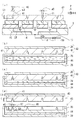
(BGA パッケージ用の保持部材の製造方法)
本発明の実施形態1に係る保持部材の製造方法について図2〜3を参照して説明する。まず、図2(b)に示されるように、硬質板からなる板状部材21を準備する。板状部材21は、保持部材を製造するため使用される成形型の原材料である。板状部材21の平面形状は、BGA 用封止済基板1の平面形状を含むことが好ましい。板状部材21としては、ガラスエポキシ基板等の複合材料板、アクリル板、フッ素樹脂板等の硬質樹脂板、アルミニウム板等の金属板、ガラス板等が使用される。
(Manufacturing method of holding member for BGA package)
A method for manufacturing the holding member according to the first embodiment of the present invention will be described with reference to FIGS. First, as shown in FIG. 2B, a plate-shaped
次に、図2(b)に示されるように、切断テーブル9の切断用ジグ10に板状部材21を一時的に固定する。図2(b)には、切断用ジグ10の上面に板状部材21が吸着によって一時的に固定される例が示される。以降の工程においては、BGA 用封止済基板1を切断する際に使用される切断テーブル9を使用できる。
Next, as shown in FIG. 2B, the plate-shaped
次に、円板状の回転刃22を準備する。回転刃22は、幅(厚さ)w2を有する溝形成用の回転刃である。溝形成用の回転刃22の幅(厚さ)w2は、切断用の回転刃18の幅(厚さ)w1よりも大きい。図2(c)に示されるように、回転刃22を直径方向に沿って切断した場合における回転刃22の外縁の断面形状は長方形状である。
Next, the disk-shaped rotary blade 22 is prepared. The rotary blade 22 is a rotary blade for forming a groove having a width (thickness) w2. The width (thickness) w2 of the rotary blade 22 for forming a groove is larger than the width (thickness) w1 of the
次に、図2(c)に示されるように、高速で回転する回転刃22を使用して板状部材21に溝部23を形成する。形成された溝部23は幅w2を有する。具体的には、BGA 用封止済基板1に仮想的に設定された複数の第1切断線7と複数の第2切断線8とに相当する(図1(a)参照)切断線24に沿って、板状部材21に溝部23を形成する。溝部23の深さは距離Lbである。距離Lbは、突起状電極6がBGA 用封止済基板1の他方の面2bから突出する突出量である距離Laよりも大きい。ここまでの工程により、保持部材を製造するため使用される成形型の一部分を構成する溝付板25が完成する。板状部材21に溝部23を形成する工程においては、BGA 用封止済基板1を切断する際に使用される切断装置が転用されてもよい。この場合には、切断装置の回転刃を交換するだけでよい。したがって、新たな加工装置を準備する必要がないので好都合である。
Next, as shown in FIG. 2C, the
次に、図3(a)に示されるように、溝付板25における溝部23が形成された面の反対面(図3(a)では上面)に、補強板26を固定する。溝付板25と補強板26とは、保持部材を製造するため使用される成形型27を構成する。補強板26の材料は、板状部材21に使用された材料から選べばよい。溝付板25に補強板26を固定する場合には、接着剤等を使用できる。
Next, as shown in FIG. 3A, the reinforcing
次に、図3(a)に示されるように、箱状部材28を準備する。箱状部材28に樹脂材料29を供給する。樹脂材料29は、常温で流動性を有する樹脂(以下「液状樹脂」という。)であって、粘度の程度を問わない。樹脂材料29は常温硬化型樹脂であることが好ましい。樹脂材料29としては、シリコーン樹脂、フッ素樹脂などが使用される。求められる保持部材の硬度や形状などに対応して、最適な樹脂材料を選択できる。樹脂材料29の内部には気泡が含まれている可能性があるので、予め脱泡して気泡を除去することが好ましい。
Next, as shown in FIG. 3A, the box-shaped
次に、図3(b)に示されるように、箱状部材28に供給された樹脂材料29に、成形型27が有する溝付板25における溝部23が形成された面の側を浸ける。溝付板25が樹脂材料29に浸けられる長さを、溝付板25における溝部23が樹脂材料29によって満たされる長さ以上に設定する。
Next, as shown in FIG. 3B, the
次に、樹脂材料29を硬化させて硬化樹脂30を成形する。図3(c)に示されるように、成形型27から硬化樹脂30を引き離す。樹脂材料29は常温硬化型樹脂であることから、硬化樹脂30が成形される過程において硬化樹脂30の収縮は発生しない。したがって、良好な寸法精度を有する硬化樹脂30が得られる。
Next, the
ここまでの工程により、箱状部材28と硬化樹脂30とを含む成形品31が完成する。成形品31は、図1に示された複数の領域3にそれぞれ対応する複数の凹部32と、複数の領域3の境界である複数の第1切断線7と複数の第2切断線8とに対応する壁部33とを、有する。凹部32は、壁部33によって囲まれた空間である。成形品31の壁部33は、成形型27の溝部23の形状が転写されることによって形成される。成形品31の凹部32は、成形型27における溝部23によって囲まれた部分(言い換えれば溝部23によって囲まれた凸部)の形状が転写されることによって形成される。
By the steps up to this point, the molded
次に、成形品31に貫通穴34(図3(d)参照)を形成する。ドリル、レーザ等を使用して、各凹部32の中央部において箱状部材28と硬化樹脂30とを貫通する貫通穴34を形成する。貫通穴34は、保持対象品を吸引する吸引穴として機能する。成形品31に貫通穴34を形成する工程によって、図3(d)に示されるように、箱状部材28と硬化樹脂30と貫通穴34とを含む保持部材35が完成する。
Next, a through hole 34 (see FIG. 3D) is formed in the molded
保持部材35が有する壁部33の幅は溝形成用の回転刃22の幅(厚さ)に等しい幅w2である。図3(c)、(d)に示される壁部33の端面36(図3(d)では下面)は水平面である。成形型27が有する溝付板25の溝部23の深さである距離Lbは、壁部33の高さに等しい。
The width of the
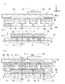
(保持部材を使用してBGA パッケージを保持する態様)
図3(d)を参照して、保持部材35を使用してBGA パッケージ19を保持する態様を説明する。保持部材35は、例えば、アンローダ等の搬送機構37に取り付けられて使用される。まず、図3(d)に示されるように、保持部材35が取り付けられた搬送機構37を準備する。
(Aspect for holding the BGA package using a holding member)
A mode of holding the
次に、切断テーブル9に吸着されたBGA パッケージ19の上方に保持部材35を移動させた後に、保持部材35を下降させる。この工程においては、切断テーブル9と搬送機構37とを相対的に昇降すればよい。この過程において、隣り合うBGA パッケージ19同士の間におけるすき間20の中心と壁部33の中心とを位置合わせする。位置合わせ後の状態でZ方向に沿って見る(以下「平面視する」という。)場合において、壁部33とBGA パッケージ19とが重なる長さ(図3(d)においてはX方向に沿って重なる長さとして示される)は、距離L1である。
Next, after moving the holding
次に、図3(d)に示されるように、配管38と弁(図示なし)とを順次経由して、吸気VJによって各BGA パッケージ19を吸引する。これにより、壁部33の端面36において各BGA パッケージ19の外周部が吸着される。
Next, as shown in FIG. 3D, each
次に、切断テーブル9における吸引(図2に示された吸気VT参照)を停止した後に、搬送機構37を上昇させて各BGA パッケージ19を次の工程を行う機構まで搬送する。次の工程を行う機構としては、例えば、検査機構、洗浄機構等が挙げられる。
Next, after stopping the suction on the cutting table 9 (see the intake VT shown in FIG. 2), the
以下、保持部材35の特徴を説明する。第1に、図3(d)に示される壁部33の端面36(図3(d)では下面。以下同じ。)は水平面である。
Hereinafter, the features of the holding
第2に、壁部33は幅w2を有する。壁部33の幅w2と、BGA パッケージ19同士の間のすき間20の幅w1(=切断用の回転刃の幅w1)との関係は、幅w2>幅w1である。
Second, the
第3に、隣り合うBGA パッケージ19同士の対向する外周部(以下適宜「対向する外周部」という。)に壁部33の端部39(図3(d)では下部であって、破線によって囲まれた部分。以下同じ。)における端面36が押し当てられる。このことによって、対向する外周部と壁部33の端面36とが密着する。これにより、壁部33の端部39が圧縮されてX方向及びY方向に広がるようにして変形する。したがって、各BGA パッケージ19の外周部が吸着された状態において、壁部47とBGA パッケージ19とが重なる長さは、図3(d)に示された距離L1よりも大きい。硬化樹脂30の硬度は、BGA パッケージ19の対向する外周部に壁部33の端部39が押し当てられることによって壁部33の端部39が押しつぶされるように変形する程度の硬度に、設定される。
Thirdly, the
上述した3つの特徴によって、壁部33の端面36がBGA パッケージ19同士の間のすき間20を塞ぐ。この状態において、硬化樹脂30の外底面(図3(d)では上側の面)から硬化樹脂30の内底面(図3(d)では凹部32における上側の面)を見る場合において、言い換えれば平面視する場合において、各BGA パッケージ19が各凹部32を完全に包含する。吸気VJを使用して各BGA パッケージ19が吸引されることによって、保持部材35が有する各壁部33の端面36に各BGA パッケージ19の外周部が吸着される。保持部材35は吸着ジグとして機能する。
Due to the above three features, the
加えて、保持部材35が有する凹部32の深さである距離Lbは、突起状電極6がBGA 用封止済基板1の他方の面2bから突出する突出量である距離Laよりも大きい。距離Lbは、壁部33の端部39が押しつぶされるように変形した場合においても、保持部材35が有する凹部32の内底面が突起状電極6の頂部に接触しない程度に大きいことが好ましい。これにより、第1に、保持部材35が有する凹部32の内底面が突起状電極6の頂部に接触することによってBGA パッケージ19の対向する外周部と壁部33の端部39とが離れる事態が、回避される。したがって、吸気VJが漏れることに起因してBGA パッケージ19が吸着されなくなる事態が、回避される。
In addition, the distance Lb, which is the depth of the
第2に、距離Lbを適切な大きさに設定することによって、BGA パッケージ19の対向する外周部と壁部33の端面36とが密着した状態で、各BGA パッケージ19の突起状電極6は、保持部材35が有する各凹部32に完全に収容される。したがって、各BGA パッケージ19の外周部は、保持部材35が有する各凹部32を取り巻く壁部33の端面36に吸着される。
Secondly, by setting the distance Lb to an appropriate size, the protruding
保持部材35が有する各凹部32の内底面が突起状電極6の頂部に接触した場合においては、BGA パッケージ19の対向する外周部と壁部33の端面36とが密着する状態が保たれればよい。この場合には、各BGA パッケージ19が有する他方の面2bにおいて突起状電極6以外の部分の空間が連通する。したがって、BGA パッケージ19の対向する外周部と壁部33の端面36とが密着した状態で、各BGA パッケージ19は、保持部材35が有する各凹部32を取り巻く壁部33の端面36に吸着される。
When the inner bottom surface of each
(作用効果)
本実施形態によれば、保持部材35において複数のBGA パッケージ19が吸着されて保持される壁部33と、壁部33に取り巻かれた複数の凹部32を、一括して形成できる。したがって、複数の凹部32を有する保持部材35を安価に製造できる。
(Action effect)
According to the present embodiment, the
本実施形態によれば、樹脂材料29として常温硬化型樹脂を使用して、保持部材35に含まれる硬化樹脂30を成形する。これにより、硬化樹脂30が成形される過程において硬化樹脂30の収縮は発生しない。したがって、良好な寸法精度を有する保持部材35を製造できる。
According to this embodiment, a room temperature curable resin is used as the
本実施形態によれば、箱状部材28と硬化樹脂30とを含む保持部材35が一括して製造できる。箱状部材28は、保持部材35の補強材として機能する。箱状部材28は、必要に応じて保持部材35を他の部材(例えば、製造装置が有する搬送機構37(図3(d)参照)を構成する部材)に固定するための固定板としても機能する。したがって、補強材及び固定板として機能する部材を備えた保持部材35を安価に製造できる。
According to this embodiment, the holding
(変形例)
以下の変形例を採用してもよい。これらの変形例は、他の実施形態においても適宜に採用されることができる。
(Modification example)
The following modification may be adopted. These modifications can be appropriately adopted in other embodiments as well.
第1に、硬化樹脂30からなる成形品が成形された後に、箱状部材28から硬化樹脂30を取り外してもよい。この場合には、箱状部材28を繰り返し成形用ジグとして使用できるという利点が生じる。硬化樹脂30の硬度を適当に大きく設定することによって、硬化樹脂30単体を保持部材35として使用できる。必要に応じて硬化樹脂30を他の部材(例えば、製造装置が有する搬送機構37(図3(d)参照)を構成する部材)に固定して、その部材に固定された硬化樹脂30を保持部材として機能させてもよい。
First, the cured
第2に、箱状部材28を使用せずに、板状部材の上に大きな粘度を有する樹脂材料29を供給してもよい。この場合には、樹脂材料29の粘度は、板状部材の上に樹脂材料29が供給された状態で板状部材を傾けても樹脂材料29が静止した状態を保つ程度に大きいことが、好ましい。成形型27が有する溝付板25における溝部23が形成された面の側を、大きな粘度を有する樹脂材料29に浸ける。大きな粘度を有する樹脂材料29を硬化させて硬化樹脂30を成形する工程以降は、これまで説明した工程に同じである。
Secondly, the
この変形例においては、まず、大きい平面形状を有する板状部材を使用して、硬化樹脂30を成形する。次に、板状部材と硬化樹脂30とを含む成形品に対して保持部材として必要な範囲を設定して、必要な範囲と不要な外周部との境界を切断する。これにより、保持部材として必要な範囲に相当する、板状部材と硬化樹脂30とを含む保持部材35が完成する。
In this modification, first, the cured
第3に、樹脂材料29として、常温で流動性を有する樹脂に代えて、次のような樹脂材料を使用してもよい。その樹脂材料は、成形型27が有する溝付板25における溝部23の形状が転写される程度に変形できる特性と、溝部23の形状が転写された状態で常温において硬化する特性とを有する樹脂材料である。例えば、樹脂材料29としてゼリー状の樹脂材料を使用できる。
Thirdly, as the
第4に、壁部33の端面36を、大きい曲率半径(言い換えれば、小さい曲率)を有する曲面にしてもよい。この場合においても、BGA パッケージ19の対向する外周部に壁部33の端部39が押し当てられることによって壁部33の端部39が押しつぶされるように変形する。したがって、壁部33の端面36がBGA パッケージ19同士の間のすき間20を塞ぐことができる。
Fourth, the
第5に、硬化樹脂30を2層構造にしてもよい。図3(a)に示された箱状部材28に第1の樹脂材料を供給して第1の硬化樹脂を成形した後に、第1の硬化樹脂の上に第2の樹脂材料を供給して第2の硬化樹脂を成形する。第2の硬化樹脂の硬度は第1の硬化樹脂の硬度よりも小さい。この変形例によれば、軟らかく変形しやすい第2の硬化樹脂が硬い第1の硬化樹脂によって支持され、かつ、第2の硬化樹脂によって壁部33の端部39が構成される。
Fifth, the cured
この変形例によれば、壁部33の端部39が軟らかく変形しやすいことによって、壁部33の端面36がBGA パッケージ19同士の間のすき間20をいっそう確実に塞ぐことができる。大きい硬度を有する第1の硬化樹脂は、保持部材35における補強板として機能し、かつ、必要に応じて保持部材35を他の部材に固定するための固定板としても機能する。第1の樹脂材料を硬化させて第1の硬化樹脂を成形することに代えて、第2の硬化樹脂よりも大きい硬度を有する硬質樹脂からなる樹脂板を、予め箱状部材28の内底面に供給してもよい。
According to this modification, the
〔実施形態2〕
(BGA パッケージ用の保持部材の製造方法)
本発明の実施形態2に係る保持部材の製造方法を、図4を参照して説明する。これまで説明した実施形態における内容と同じ内容の説明を適宜省略する。
[Embodiment 2]
(Manufacturing method of holding member for BGA package)
A method for manufacturing the holding member according to the second embodiment of the present invention will be described with reference to FIG. The description of the same contents as those in the embodiments described above will be omitted as appropriate.
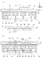
まず、板状部材21(図2(b)参照)を準備する。図4(a)に示された円板状の回転刃40を準備する。回転刃40は、幅(厚さ)w3を有する溝形成用の回転刃である。図4(a)に示されるように、回転刃40を直径方向に沿って切断した場合における回転刃40の外縁の断面形状はV字状である。溝形成用の回転刃40の幅(厚さ)w3は、図2(a)に示された切断用の回転刃18の幅(厚さ)w1よりも大きい。回転刃40の幅w3は、図2(c)に示された溝形成用の回転刃22の幅(厚さ)w2よりも小さいことが好ましい。
First, the plate-shaped member 21 (see FIG. 2B) is prepared. The disk-shaped
次に、回転刃40を使用して板状部材に溝部41を形成する。形成された溝部41は幅w3を有する。溝部41の底付近の断面形状はV字状である。溝部41の深さは距離Lbである。距離Lbは、図2(a)に示された突起状電極6がBGA 用封止済基板1の他方の面2bから突出する突出量である距離Laよりも大きい。ここまでの工程により、保持部材を製造するため使用される成形型の一部分を構成する溝付板42が完成する。
Next, the
次に、図4(b)に示されるように、溝付板42における溝部41が形成された面の反対面(図4(b)では上面)に、補強板26を固定する。溝付板42と補強板26とは、保持部材を製造するため使用される成形型43を構成する。
Next, as shown in FIG. 4B, the reinforcing
次に、図4(b)に示されるように、箱状部材28を準備する。箱状部材28には、内底面に樹脂板44が予め供給される。樹脂板44は、硬質樹脂からなる樹脂材料である。樹脂板44の上に、液状樹脂からなる樹脂材料29を供給する。箱状部材28に供給された樹脂材料29の上に、溝付板42を下側にして成形型43を配置する。
Next, as shown in FIG. 4B, the box-shaped
次に、図4(c)に示されるように、箱状部材28に供給された樹脂材料29に、成形型43が有する溝付板42における溝部41が形成された面の側を浸ける。溝付板42が樹脂材料29に浸けられる長さを、溝付板42における溝部41が樹脂材料29によって満たされる長さ以上に設定する。
Next, as shown in FIG. 4C, the
次に、樹脂材料29を硬化させて硬化樹脂30を成形する。この過程において、硬質樹脂からなる樹脂板44と硬化樹脂30とが接着される。硬化樹脂30の硬度は樹脂板44の硬度よりも小さい。
Next, the
次に、図4(d)に示されるように、成形型43から硬化樹脂30を引き離す。樹脂材料29は常温硬化型樹脂であるので、硬化樹脂30が成形される過程において硬化樹脂30の収縮は発生しない。したがって、良好な寸法精度を有する硬化樹脂30が得られる。
Next, as shown in FIG. 4D, the cured
ここまでの工程によって、箱状部材28と、硬質樹脂からなる樹脂板44と、硬化樹脂30とを含む成形品45が完成する。樹脂板44は土台であって、第1の層に相当する。硬化樹脂30は、樹脂板44を覆うようにして成形され、第2の層に相当する。成形品45は、図1に示された複数の領域3にそれぞれ対応する複数の凹部46と、複数の領域3の境界である複数の第1切断線7と複数の第2切断線8(図1(a)参照)とに対応する壁部47とを、有する。凹部46は、壁部47によって囲まれた空間である。
By the steps up to this point, the molded
次に、図5(a)に示されるように、成形品45に貫通穴48を形成する。ドリル、レーザ等を使用して、各凹部46の中央部において箱状部材28と樹脂板44と硬化樹脂30とを貫通する貫通穴48を形成する。貫通穴48は、保持対象品を吸引する吸引穴として機能する。成形品45に貫通穴48を形成する工程によって、箱状部材28と硬化樹脂30と樹脂板44と貫通穴48とを含む保持部材49が完成する。
Next, as shown in FIG. 5A, a through
図5を参照して、保持部材49が有する壁部47の寸法形状を以下に説明する。壁部47の幅は、溝形成用の回転刃40の幅(厚さ)に等しい幅w3である。壁部47の端部50(図5では下部。以下同じ。)は、先端51(図5では下端。以下同じ。)に近づくほど幅が狭い。言い換えれば、壁部47の端部50の断面形状(図5のX軸に沿って切断した場合の断面形状)は、図5に示された状態で(端部50を下にした状態で)V字状である。壁部47の先端51は、図5のY軸に沿って伸びる稜線である。溝付板42における溝部41の深さである距離Lbは、保持部材49においては壁部47の高さに等しい。壁部47の側面を曲面にしてもよい。小さい曲率半径(言い換えれば、大きい曲率)を有する曲面を先端51に設けてもよい。
With reference to FIG. 5, the dimensions and shape of the
(保持部材を使用してBGA パッケージを保持する態様)
図5を参照して、保持部材49を使用してBGA パッケージ19を保持する工程を説明する。まず、図5(a)に示されるように、保持部材49が取り付けられた搬送機構37を準備する。
(Aspect for holding the BGA package using a holding member)
The process of holding the
次に、図5(a)に示されるように、切断テーブル9に吸着されたBGA パッケージ19の上方に保持部材49を移動させる。この過程において、隣り合うBGA パッケージ19同士の間におけるすき間20の中心と壁部47の中心とを、位置合わせする。
Next, as shown in FIG. 5A, the holding
次に、図5(a)に示される状態から、搬送機構37を下降させる。この工程においては、切断テーブル9と搬送機構37とを相対的に昇降すればよい。これにより、隣り合うBGA パッケージ19同士の間におけるすき間20に、壁部47の端部50が挿入される。壁部47の端部50は、図5に示された状態でV字状の断面形状を有する。壁部47の先端51を含む端部50の一部分がすき間20の内部(図5ではすき間20の最上端よりも下側の部分)に入り込み、壁部47における変形した両側面がすき間20の最上端に密着する。したがって、壁部47によってすき間20を塞ぐことができる。この状態で平面視する場合において、各BGA パッケージ19が各凹部46を完全に包含する。壁部47の先端51を含む一部分がすき間20の内部に入り込んだ状態において凹部46の内底面(図5(b)では凹部46における上側の面)と突起状電極6の頂部とが接触しないように、距離Lbが定められることが好ましい。
Next, the
次に、図5(b)に示されるように、吸気VJによって各BGA パッケージ19を吸引する。これにより、壁部47の端部50における両側面において各BGA パッケージ19が吸着される。保持部材49は吸着ジグとして機能する。
Next, as shown in FIG. 5 (b), each
次に、切断テーブル9における吸引を停止した後に、搬送機構37を上昇させて各BGA パッケージ19を次の工程を行う機構まで搬送する。
Next, after stopping the suction on the cutting table 9, the
(作用効果)
本実施形態によれば、実施形態1と同様の効果が得られる。加えて、本実施形態によれば次の効果が得られる。軟らかく変形しやすい壁部47の端部50が、先端51に近づくほど幅が狭い断面形状を有する。壁部47の先端51がすき間20の内部に入り込むことによって、壁部47における変形した両側面がすき間20を塞ぐ。一方、図3(d)に示されるように、実施形態1によれば、壁部33の端部39が押しつぶされるように変形してすき間20を塞ぐ。したがって、本実施形態によれば、平面視して壁部47とBGA パッケージ19とが重なる長さ(図5(b)においてはX方向に沿って重なる長さL2として示される)が実施形態1における重なる長さL1(図3(d)参照)よりも小さい。実施形態1に比較して本実施形態によれば、隣り合うBGA パッケージ19同士における外縁のいっそう近くまで突起状電極6を配置できる。したがって、本実施形態は、BGA パッケージ19における突起状電極6の配置の更なる高密度化を可能にする。
(Action effect)
According to the present embodiment, the same effect as that of the first embodiment can be obtained. In addition, according to this embodiment, the following effects can be obtained. The
本実施形態がBGA パッケージ19における突起状電極6の配置の更なる高密度化を可能にすることは、図3(d)と図5(b)とを比較すれば明らかである。実施形態1を示す図3(d)においては、1個のBGA パッケージ19においてX方向に沿って4個の突起状電極6が配置される。一方、本実施形態を示す図5(b)においては、1個のBGA パッケージ19においてX方向に沿って5個の突起状電極6が配置される。
It is clear by comparing FIGS. 3 (d) and 5 (b) that this embodiment enables further densification of the arrangement of the protruding
加えて、本実施形態によれば、BGA パッケージ19の外縁と最も外側のはんだボールの最も外側の縁との間の距離が小さい場合においても、各BGA パッケージ19が保持部材49に吸着される。このことは、第1に、BGA パッケージ19の小型化を可能にする。第2に、同じ平面積を有するBGA 用封止済基板1(図1参照)から製造されるBGA パッケージ19の数、言い換えれば、BGA パッケージ19の取れ数の増大を可能にする。
In addition, according to the present embodiment, each
(変形例)
変形例として、図4(b)に示された箱状部材28に第1の樹脂材料を供給して第1の硬化樹脂を成形した後に、第1の硬化樹脂の上に第2の樹脂材料を供給して第2の硬化樹脂を成形してもよい。第2の硬化樹脂の硬度は第1の硬化樹脂の硬度よりも小さい。壁部47における端部50付近を第2の硬化樹脂によって形成し、端部50の付近よりも箱状部材28に近い部分を第1の硬化樹脂によって形成してもよい。これらの構成により、軟らかく変形しやすい第2の硬化樹脂が硬い第1の硬化樹脂によって支持され、かつ、第2の硬化樹脂によって壁部47の端部50が構成される。したがって、壁部47における端部50が軟らかく変形しやすいことによって、端部50がBGA パッケージ19同士の間のすき間20をいっそう確実に塞ぐことができる。
(Modification example)
As a modification, after supplying the first resin material to the box-shaped
先端51の角度を鋭角にすることが好ましく、先端51の角度を15°以上で45°以下にすることが更に好ましい。先端51の角度を15°以上で45°以下にすることが更に好ましい理由は次の通りである。先端51の角度を15°未満にした場合には、壁部47がすき間20の内部に深く入り込むことによって、保持部材49が有する凹部46の内底面が突起状電極6の頂部に接触する可能性がある。この場合は、BGA パッケージ19の対向する外周部と壁部47の端部50とが離れてBGA パッケージ19の吸着を不可能にするおそれがあるので、好ましくない。先端51の角度を45°よりも大きくした場合は、突起状電極6の配置の高密度化及びBGA パッケージ19の小型化を妨げるので、好ましくない。
The angle of the
壁部47に関して以下の変形例を採用してもよい。端部50の断面形状を、先端51に近づくほど幅が狭くなっている非対称の形状にしてもよい。例えば、端部50の断面形状を、角記号∠を反時計回りに90°回転させた形状にしてもよい。
The following modification may be adopted for the
〔実施形態3〕
(保持部材を使用してLED パッケージを保持する態様)
本発明の実施形態3に係る保持部材が光素子を保持する態様を、図6を参照して説明する。図6には、保持対象品として、光学製品に相当するLED (Light emitting diode )パッケージ52が示される。LED パッケージ52は、プリント基板、リードフレーム等からなる基板53と、LED チップ54と、凸部に相当する封止樹脂55とを有する。透光性樹脂から構成される封止樹脂55は、凸レンズとして機能する。基板53が有する一方の面(図6(a)においては下面)には外部端子(図示なし)が形成される。基板53が有する他方の面56(図6(a)においては上面)がチップ装着面である。基板53の他方の面56から突出する封止樹脂55の頂部までの高さは(言い換えれば封止樹脂55の突出量は)、距離Laである。LED パッケージ52は、LED 用封止済基板(図示なし。図1に示されたBGA 用封止済基板1に相当する。)が個片化されることによって製造される。1個のLED パッケージ52が有する封止樹脂55は、保持部材49に成形された複数の凹部46のうちの1個の凹部46に収容される。
[Embodiment 3]
(Aspect for holding the LED package using a holding member)
A mode in which the holding member according to the third embodiment of the present invention holds the optical element will be described with reference to FIG. FIG. 6 shows an LED (Light emitting diode)
図6に示されたLED パッケージ52は、X方向に沿って2個、Y方向に沿って2個、合計4個のLED チップ54を有する。1個のLED パッケージ52に1個のLED チップ54が設けられてもよい。光素子として、LED チップ54に代えてレーザダイオードチップが設けられてもよい。1個のパッケージに、1個の発光素子と1個の受光素子とが設けられてもよい。この場合には、その1個のパッケージが光学センサとして機能する。
The
図6に示された保持部材49は、図5に示された保持部材49と同じ態様でLED パッケージ52を保持する。図6(b)に示された状態で平面視する場合において、各LED パッケージが各凹部46を完全に包含する。この場合においては、封止樹脂55の突出量である距離Laと、壁部47の先端51を含む一部分がすき間20の内部に入り込む量とを考慮して、凹部46の深さである距離Lbが定められる。具体的には、壁部47の先端51を含む一部分がすき間20の内部に入り込んだ状態で凹部46の内底面(図6(b)では凹部46における上側の面)と封止樹脂55の頂部とが接触しないように、距離Lbが定められる。
The holding
(作用効果)
本実施形態によれば、基板53における他方の面56において基板53の外縁と封止樹脂55の外縁との間の距離が小さい場合においても、各LED パッケージ52が保持部材49に吸着される。このことは、第1に、LED パッケージ52の小型化を可能にする。第2に、同じ平面積を有するLED 用封止済基板から製造されるLED パッケージ52の数、言い換えれば、LED パッケージ52の取れ数の増大を可能にする。
(Action effect)
According to this embodiment, each
〔実施形態4〕
(切断装置の構成)
図7を参照して、図1に示したBGA 用封止済基板1を切断する切断装置の構成について説明する。図7に示された切断装置57は、図3(d)に示された保持部材35を使用して製品であるBGA パッケージ19を製造する、製品の製造装置の1つの形態である。
[Embodiment 4]
(Configuration of cutting device)
A configuration of a cutting device for cutting the sealed
図7に示されるように、切断装置57は、BGA 用封止済基板1を供給する供給モジュールAと、BGA 用封止済基板1を切断する切断モジュールBと、切断されたBGA パッケージ19を検査して保管する検査・保管モジュールCとを、それぞれ構成要素として備える。各構成要素(各モジュールA〜C)は、それぞれ他の構成要素に対して着脱可能かつ交換可能である。
As shown in FIG. 7, the cutting
供給モジュールAには、BGA 用封止済基板1を供給する封止済基板供給部58が設けられる。BGA 用封止済基板1は、搬送機構(図示なし)によって、BGA 用封止済基板1における他方の面2b(突起状電極6が形成された面;図1参照)を上向き(+Z方向の向き)にして、供給モジュールAから切断モジュールBに搬送される。
The supply module A is provided with a sealed
切断モジュールBには、BGA 用封止済基板1を載置して切断するための切断テーブル9(図2参照)が設けられる。切断テーブル9の上には切断用ジグ10(図2参照)が取り付けられる。切断テーブル9は、移動機構59によって図のY方向に移動可能である。かつ、切断テーブル9は、回転機構60によってθ方向に回転可能である。切断テーブル9の上に取り付けられた切断用ジグ10の上にBGA 用封止済基板1が載置される。
The cutting module B is provided with a cutting table 9 (see FIG. 2) for placing and cutting the sealed
切断モジュールBには、切断機構としてスピンドル61が設けられる。スピンドル61は、独立してX方向及びZ方向に移動可能である。スピンドル61にはBGA 用封止済基板1を切断する回転刃18が装着される。図2(a)にも示されるように、回転刃18は幅(厚さ)w1を有する。
The cutting module B is provided with a
スピンドル61には、高速回転する回転刃18に向かって切削水を噴射する切削水用ノズル、冷却水を噴射する冷却水用ノズル(どちらも図示なし)等がそれぞれ設けられる。切断テーブル9とスピンドル61とを相対的に移動させることによってBGA 用封止済基板1が切断される。回転刃18は、Y−Z平面の面内において回転することによってBGA 用封止済基板1を切断する。
The
切断装置57は、1個のスピンドル61が設けられるシングルスピンドル構成の切断装置である。これに限らず、切断モジュールBに2個のスピンドルが設けられるツインスピンドル構成を有する切断装置にしてもよい。更に、切断テーブルを2個設けて、それぞれの切断テーブルにおいてBGA 用封止済基板1を切断するツインカットテーブル構成にしてもよい。ツインスピンドル構成及びツインカットテーブル構成を採用することによって、切断装置の生産性を向上させることができる。
The cutting
検査・保管モジュールCには、BGA 用封止済基板1を切断して個片化された複数のBGA パッケージ19を吸着して搬送する搬送機構37(図3(d)参照)が設けられる。搬送機構37は、X方向及びZ方向に移動可能である。搬送機構37には、図3(d)に示された保持部材35が取り付けられる。搬送機構37は、保持部材35を使用して、個片化された複数のBGA パッケージ19を保持部材35に一括して吸着して搬送する。
The inspection / storage module C is provided with a transport mechanism 37 (see FIG. 3 (d)) for sucking and transporting a plurality of BGA packages 19 which are separated from the sealed
検査・保管モジュールCには、個片化された複数のBGA パッケージ19を載置して検査するための検査テーブル62が設けられる。検査テーブル62の上には検査用ジグ63が取り付けられる。検査テーブル62はY軸を軸にして回転することができ、X方向及びZ方向に移動可能である。搬送機構37によって、複数のBGA パッケージ19は検査用ジグ63の上に一括して載置される。複数のBGA パッケージ19は、検査用カメラ64によって、図5(a)に示された封止樹脂5の表面(図5(a)では下面)及び突起状電極6の側の面である他方の面2bが、それぞれ検査される。
The inspection / storage module C is provided with an inspection table 62 for mounting and inspecting a plurality of individualized BGA packages 19. An
検査・保管モジュールCには、検査された複数のBGA パッケージ19を一時的に保管するための保管テーブル65が設けられる。保管テーブル65はY方向に移動可能である。保管テーブル65には、実施形態2に示されたBGA パッケージ用の保持部材35が取り付けられる。保管テーブル65は保持機構に相当する。検査されたBGA パッケージ19は検査テーブル62から一括して保管テーブル65に取り付けられた保持部材35に移載される。保管テーブル65に保管されたBGA パッケージ19は良品と不良品とに区別され、移送機構(図示なし)によって良品は良品用トレイ66に、不良品は不良品用トレイ67にそれぞれ移送されて収納される。
The inspection / storage module C is provided with a storage table 65 for temporarily storing a plurality of inspected BGA packages 19. The storage table 65 is movable in the Y direction. The holding
供給モジュールAには制御部CTLが設けられる。制御部CTLは、切断装置57の動作、BGA 用封止済基板1の搬送、BGA 用封止済基板1の切断、個片化されたBGA パッケージ19の搬送、BGA パッケージ19の検査、BGA パッケージ19の収納等を制御する。本実施形態においては、制御部CTLを供給モジュールAに設けた。これに限らず、制御部CTLを他のモジュールに設けても良い。また、制御部CTLを複数の部分に分割して、供給モジュールA、切断モジュールB及び検査・保管モジュールCのうちの少なくとも2つのモジュールに、分割された部分をそれぞれ設けても良い。
The supply module A is provided with a control unit CTL. The control unit CTL operates the cutting
図6に示されたLED パッケージ52を製造する場合には、保持部材49が取り付けられた搬送機構37を使用する。光学製品を製造する場合、例えば、マイクロレンズアレイを製造する場合には、保持部材が保持する保持対象品がマイクロレンズアレイになる。この場合には、マイクロレンズアレイの寸法形状に対応する保持部材を準備する。準備された保持部材を搬送機構に取り付けて、その保持部材にマイクロレンズアレイを吸着させる。その後に、搬送機構を使用してマイクロレンズアレイを搬送する。
When manufacturing the
本実施形態においては、保持部材35(図3(d)、図7参照)及び保持部材49(図5、6参照)は、代表的には次の工程において使用される。それは、切断されることによって個片化されたBGA パッケージ19及びLED パッケージ52とが、切断テーブルから検査テーブルに搬送される工程である。この以外の工程として、BGA パッケージ19及びLED パッケージ52とがそれぞれ有する凹凸のうち凸部(突起状電極6及び封止樹脂55)を上方に向けて、BGA パッケージ19及びLED パッケージ52とが吸着される工程において、保持部材35、49が使用される。
In the present embodiment, the holding member 35 (see FIGS. 3D and 7) and the holding member 49 (see FIGS. 5 and 6) are typically used in the following steps. It is a process in which the
(作用効果)
本実施形態によれば、切断装置57において、搬送機構37及び保管テーブル65に、実施形態2に示されたBGA パッケージ用の保持部材35を適用する。1個のBGA パッケージ19の複数の突起状電極6は、保持部材35に成形された複数の凹部32のうちの1個の凹部32に収容される。したがって、複数のBGA パッケージ19において、図5(a)に示された突起状電極6の側の面である他方の面2bを安定して搬送機構37及び保管テーブル65に吸着することができる。この保持部材35を搬送機構37及び保管テーブル65に適用することによって、切断装置57の製造コストを抑制することができる。
(Action effect)
According to the present embodiment, in the
ここまで説明した実施形態において、本発明に係る保持部材が保持する保持対象品として、BGA パッケージ19とLED パッケージ52とを例示して説明した。これらに限らず、吸着される面に凹凸を有する保持対象品に対して本発明が適用される。第1に、吸着される面において、銅箔からなる端子と、絶縁性樹脂からなるソルダーレジストとが形成された、LGA (Land grid array )用封止済基板が挙げられる。端子の厚さとソルダーレジストの厚さとは通常異なるので、LGA (Land grid array )用封止済基板における吸着される面には、凹凸(言い換えれば段差)が形成される。第2に、吸着される面においてレンズが形成された光学製品が挙げられる。凸部の例として凸レンズが、凹部の例として凹レンズが、凹凸の例としてフレネルレンズが、それぞれ挙げられる。光学製品には、マイクロレンズアレイが含まれる。
In the embodiments described so far, the
ここまで説明した実施形態においては、保持部材を製造する際に、図3(a)〜(c)に示された成形型27及び図4(b)〜(d)に示された成形型43を使用した。成形型27は溝付板25(図3(a)〜(c)参照)を有する。成形型43は、溝付板42(図4参照)を有する。溝付板25、42を製作する際に、幅(厚さ)w2を有する円板状の回転刃22を使用して、硬質樹脂板等からなる板状部材21に溝を形成した。板状部材21に代えて、個片化される直前の中間製品に対して回転刃22、40を使用して溝部を形成してもよい。個片化される直前の中間製品としては、第1に、BGA 用封止済基板1自体(図1参照)が挙げられる。第2に、LED パッケージ52(図6参照)に個片化される直前のLED パッケージ用封止済基板自体(図示なし)が挙げられる。第3に、マイクロレンズアレイ等の光学製品を製造する過程における、マイクロレンズアレイ等に個片化される直前の中間製品である、成形品が挙げられる。
In the embodiments described so far, when the holding member is manufactured, the molding dies 27 shown in FIGS. 3 (a) to 3 (c) and the molding dies 43 shown in FIGS. 4 (b) to 4 (d) are formed. It was used. The
上述した封止済基板と同じ寸法形状を有する代替品に、回転刃22、40を使用して溝部を形成してもよい。代替品として、例えば、図1に示されたBGA 用封止済基板1の代替品になる成形品が挙げられる。この成形品を製造するために、BGA 用封止済基板1に使用される基板2と同じ基板を使用して、例えば、チップ4を装着することなく、封止樹脂5と同じ寸法形状を有するダミー樹脂を成形する。回転刃22、40を使用してこのダミー樹脂を含む成形品に溝部を形成することによって、溝付板25、42に代わる溝付成形品を製作する。図3(a)〜(c)に示された成形型27及び図4(b)〜(d)に示された成形型43の代わりとして、溝付成形品を使用することができる。
Grooves may be formed by using
ここまで説明した実施形態において、回転刃22、40を使用して溝部23、41を形成した。溝部23、41を形成する工程において、回転刃22、40に代えて、ワイヤソー、バンドソー等を使用して加工してもよい。更に、溝部23、41を形成する工程において、レーザ加工、ブラスト加工、ウォータージェット加工等を使用してもよい。ワイヤソーによる加工、レーザ加工、ブラスト加工、ウォータージェット加工を使用する場合には、平面形状に曲線又は折れ線が含まれる製品を製造することができる。平面形状に曲線又は折れ線が含まれる製品の例として、メモリーカードが挙げられる。
In the embodiments described so far, the
ここまで説明した実施形態において、保持部材49を吸着ジグとして使用した。変形例として、吸引穴48が形成されない部材である成形品45(図4(d)参照)を、トレイとして使用できる。言い換えれば、成形品45は、吸引穴を必要としない保持部材として使用され得る。図4(d)に示された成形品45がトレイとして使用される態様を説明する。図4(d)に示された状態(凹部46の開口が上を向いた状態)で、成形品45を使用する。図5(b)が上下反転された状態を参照して説明する。この状態において、凹部46を囲む壁部47の端部50における内側面にBGA パッケージ19が有する外縁が接触するようにして、BGA パッケージ19が凹部46に収容される。BGA パッケージ19が有する突起状電極6が凹部46の内底面に接触しない。これにより、突起状電極6に汚れが付着することが防止される。したがって、突起状電極6が関与する電気的接続が安定して行われる。加えて、BGA パッケージ19を搬送する際のがたつきが抑制される。
In the embodiments described so far, the holding
別の変形例として、図6(b)が上下反転された状態を参照して説明する。この場合には、LED パッケージ52が有する封止樹脂55が凹部46の内底面に接触しない。これにより、凸レンズとして機能する封止樹脂55に汚れが付着することが防止される。したがって、LED パッケージ52の光学的特性の低下が生じない。加えて、LED パッケージ52を搬送する際のがたつきが抑制される。
As another modification, FIG. 6B will be described with reference to the upside-down state. In this case, the sealing
更に別の変形例として、図3(c)に示された成形品31の変形例がトレイとして使用され得る。図3(a)に示された溝部23の中心に、幅(厚さ)w4を有する溝形成用の回転刃を使用して浅い溝部を形成する。回転刃の幅w4は、切断用の回転刃18の幅w1(図2(a)参照)よりも小さい。図3(a)〜(c)に示された工程によって、図3(c)に示された成形品31に代わる成形品が製造される。この成形品は、図3(c)に示された壁33の上部における両側の角部に形成された段差を有する。この段差における水平面に、BGA パッケージ19、LED パッケージ52等の保持対象品の外縁が置かれる。この変形例においても、これまで説明した2つの変形例と同様の効果が得られる。
As yet another modification, the modification of the molded
これまで説明した3つの変形例において、成形品31の変形例である成形品及び成形品45に吸引穴を形成してもよい。これらの場合には、保持部材35の変形例である保持部材及び保持部材49が、保持対象品を吸着する機能を有するトレイに相当する。
In the three modified examples described so far, suction holes may be formed in the molded product and the molded
各実施形態においては、製品の製造装置の1つの形態として、切断装置について説明した。これに限らず、それぞれ製品の製造装置において使用される、製品を搬送する搬送装置、製品を収納する収納装置、製品を検査する検査装置などにおいても、本発明の保持部材を適用することができる。 In each embodiment, the cutting device has been described as one embodiment of the product manufacturing device. Not limited to this, the holding member of the present invention can also be applied to a transport device for transporting a product, a storage device for storing the product, an inspection device for inspecting the product, and the like, which are used in the manufacturing apparatus for each product. ..
本発明は、上述した各実施形態に限定されるものではなく、本発明の趣旨を逸脱しない範囲内で、必要に応じて、任意にかつ適宜に組み合わせ、変更し、又は選択して採用できるものである。 The present invention is not limited to the above-described embodiments, and can be arbitrarily and appropriately combined, modified, or selected and adopted as necessary without departing from the spirit of the present invention. Is.
1 BGA 用封止済基板(中間製品)
2、53 基板
2a 一方の面
2b 他方の面(第1の面)
3 領域
4 チップ
5、55 封止樹脂
6 突起状電極
7 第1切断線
8 第2切断線
9 切断テーブル
10 切断用ジグ
11 金属プレート
12 樹脂シート
13 切断溝
14、34、48 貫通穴
15 空間
16、38 配管
17 弁
18、22、40 回転刃
19 BGA パッケージ(製品、保持対象品、電子デバイス)
20 すき間
21 板状部材(硬質板)
23、41 溝部
24 切断線
25、42 溝付板
26 補強板
27、43 成形型
28 箱状部材
29 樹脂材料
30 硬化樹脂
31、45 成形品
32、46 凹部
33、47 壁部
35、49 保持部材
36 端面
37 搬送機構
39、50 端部
44 樹脂板(第1の層)
51 先端
52 LED パッケージ(製品、保持対象品、電子デバイス)
54 LED チップ
56 他方の面(第1の面)
57 切断装置
58 封止済基板供給部
59 移動機構
60 回転機構
61 スピンドル
62 検査テーブル
63 検査用ジグ
64 検査用カメラ
65 保管テーブル
66 良品用トレイ
67 不良品用トレイ
a 一辺の長さ
A 供給モジュール
B 切断モジュール
C 検査・保管モジュール
CTL 制御部
L1、L2 重なる長さ
La、Lb 距離
VJ、VT 吸気
w1 幅(第2の幅)
w2、w3 幅(第1の幅)
1 BGA sealed substrate (intermediate product)
2,53
3
20
23, 41 Grooves 24 Cutting
51
54
57
w2, w3 width (first width)
Claims (9)
前記切断刃の厚みより大きな第1の幅を有し、前記個片化された後の隣接する前記保持対象品同士の隙間を塞ぐように配置される壁部に対応して形成されている複数の溝部を主面に有する成形型を準備する工程と、
前記成形型を樹脂材料に対向して配置する工程と、
前記成形型の前記主面を前記樹脂材料に押し付ける工程と、
前記樹脂材料を硬化させて硬化樹脂を形成することによって前記硬化樹脂を含む成形品を成形する工程と、
前記成形型から前記成形品を取り外す工程とを備え、
前記成形品は、前記複数の溝部が前記硬化樹脂に転写されることによって形成された複数の前記壁部に取り囲まれた凹部を複数備えた保持部材であり、
前記凹部が、前記保持対象品の前記複数の突起状電極を収容し、前記凹部を取り囲む前記壁部と前記保持対象品とによって密閉された状態で、前記保持対象品が保持される、保持部材の製造方法。 A method for manufacturing a holding member for manufacturing a holding member in which a plurality of holding target products having a plurality of protruding electrodes are held after being cut by a cutting blade and separated into pieces.
A plurality of the large first width than the thickness of the cutting blade have a, are formed corresponding to the wall portion arranged to block the clearance of the holding goods for the adjacent after the being diced The process of preparing a molding mold having a groove on the main surface of
The step of arranging the molding die facing the resin material and
The step of pressing the main surface of the molding die against the resin material and
A step of molding a molded product containing the cured resin by curing the resin material to form a cured resin.
A step of removing the molded product from the molding mold is provided.
The molded article is a holding member having a plurality of recesses surrounded by a plurality of the wall portion formed by said plurality of grooves is transferred to the cured resin,
A holding member in which the recessed product accommodates the plurality of protruding electrodes of the product to be held, and the product to be held is held in a state of being sealed by the wall portion surrounding the recess and the product to be held. Manufacturing method.
前記箱状部材に前記樹脂材料を供給する工程とを更に備え、
前記樹脂材料に押し付ける工程では、前記箱状部材に供給された前記樹脂材料に前記成形型の前記主面を押し付ける、請求項1に記載された保持部材の製造方法。 The process of preparing the box-shaped member and
Further provided with a step of supplying the resin material to the box-shaped member,
The method for manufacturing a holding member according to claim 1, wherein in the step of pressing against the resin material, the main surface of the molding die is pressed against the resin material supplied to the box-shaped member.
前記複数の溝部は、第1の方向に沿って伸びる複数の第1の溝部と、前記第1の方向と交わる第2の方向に沿って伸びる複数の第2の溝部とを含む、請求項1〜3のいずれか1項に記載された保持部材の製造方法。 The molding die includes a hard plate and the plurality of grooves formed on the main surface of the hard plate.
1. The plurality of grooves include a plurality of first grooves extending along a first direction and a plurality of second grooves extending along a second direction intersecting the first direction. The method for manufacturing a holding member according to any one of Items to 3.
前記第2の層は前記第1の層よりも軟らかい、請求項1〜4のいずれか1項に記載された保持部材の製造方法。 The steps of molding the molded product include a step of providing a first layer as a base and a step of molding a second layer formed so as to cover the first layer and capable of contacting the product to be held. Including and
The method for manufacturing a holding member according to any one of claims 1 to 4, wherein the second layer is softer than the first layer.
前記貫通穴は前記保持対象品を吸着するための吸引穴である、請求項1〜5のいずれか1項に記載された保持部材の製造方法。 A step of forming a through hole provided in the recess and penetrating at least the cured resin is further provided.
The method for manufacturing a holding member according to any one of claims 1 to 5, wherein the through hole is a suction hole for sucking the holding target product.
樹脂材料が硬化して形成され、前記保持対象品に接する接触面を有する硬化樹脂と、
前記硬化樹脂に含まれ、第1の方向に沿って伸びる複数の第1の壁部と、
前記硬化樹脂に含まれ、前記第1の方向と交わる第2の方向に沿って伸びる複数の第2の壁部と、
前記複数の第1の壁部と前記複数の第2の壁部とによって取り囲まれた凹部とを備え、
前記凹部が、前記個片化された後の隣接する前記保持対象品同士の隙間を塞ぎ、前記保持対象品の前記複数の突起状電極を収容し、前記凹部を取り囲む前記壁部と前記保持対象品とによって密閉された状態で、前記保持対象品が保持され、
前記複数の第1の壁部が有する形状は、成形型の主面において形成され、前記切断刃の厚みより大きな第1の幅を有する複数の第1の溝部の形状が前記硬化樹脂に転写された形状であり、
前記複数の第2の壁部が有する形状は、前記成形型の主面において形成され、前記切断刃の厚みより大きな前記第1の幅を有する複数の第2の溝部の形状が前記硬化樹脂に転写された形状である、保持部材。 A holding member that holds a plurality of holding objects having a plurality of protruding electrodes after being cut by a cutting blade and separated into pieces.
A cured resin formed by curing the resin material and having a contact surface in contact with the object to be retained,
A plurality of first wall portions contained in the cured resin and extending along the first direction,
A plurality of second wall portions contained in the cured resin and extending along a second direction intersecting with the first direction.
It is provided with a recess surrounded by the plurality of first wall portions and the plurality of second wall portions.
The recess closes a gap between adjacent products to be held after being individualized , accommodates the plurality of protruding electrodes of the product to be held, and surrounds the recess with the wall and the target to be held. The product to be held is held in a state of being sealed by the product, and the product to be held is held.
The shape of the plurality of first wall portions is formed on the main surface of the molding die, and the shape of the plurality of first groove portions having a first width larger than the thickness of the cutting blade is transferred to the cured resin. Shape
The shape of the plurality of second wall portions is formed on the main surface of the molding die, and the shape of the plurality of second groove portions having the first width larger than the thickness of the cutting blade is formed on the cured resin. A holding member that has a transferred shape.
A product manufacturing apparatus having the holding member according to claim 7.
Priority Applications (4)
| Application Number | Priority Date | Filing Date | Title |
|---|---|---|---|
| JP2017177223A JP6861602B2 (en) | 2017-09-15 | 2017-09-15 | Holding member, manufacturing method of holding member, holding mechanism and product manufacturing equipment |
| KR1020180080962A KR102157533B1 (en) | 2017-09-15 | 2018-07-12 | Holding member, manufacturing method of holding member, holding mechanism and manufacturing apparatus of product |
| CN201810889280.4A CN109509708B (en) | 2017-09-15 | 2018-08-07 | Holding member, method for manufacturing same, holding mechanism, and apparatus for manufacturing product |
| TW107128275A TWI726230B (en) | 2017-09-15 | 2018-08-14 | Holding member, method of manufacturing holding member, holding mechanism, and product manufacturing device |
Applications Claiming Priority (1)
| Application Number | Priority Date | Filing Date | Title |
|---|---|---|---|
| JP2017177223A JP6861602B2 (en) | 2017-09-15 | 2017-09-15 | Holding member, manufacturing method of holding member, holding mechanism and product manufacturing equipment |
Publications (3)
| Publication Number | Publication Date |
|---|---|
| JP2019051645A JP2019051645A (en) | 2019-04-04 |
| JP2019051645A5 JP2019051645A5 (en) | 2019-10-24 |
| JP6861602B2 true JP6861602B2 (en) | 2021-04-21 |
Family
ID=65745574
Family Applications (1)
| Application Number | Title | Priority Date | Filing Date |
|---|---|---|---|
| JP2017177223A Active JP6861602B2 (en) | 2017-09-15 | 2017-09-15 | Holding member, manufacturing method of holding member, holding mechanism and product manufacturing equipment |
Country Status (4)
| Country | Link |
|---|---|
| JP (1) | JP6861602B2 (en) |
| KR (1) | KR102157533B1 (en) |
| CN (1) | CN109509708B (en) |
| TW (1) | TWI726230B (en) |
Families Citing this family (4)
| Publication number | Priority date | Publication date | Assignee | Title |
|---|---|---|---|---|
| JP6952737B2 (en) * | 2019-05-24 | 2021-10-20 | Towa株式会社 | Holding member, inspection mechanism, cutting device, manufacturing method of holding object and manufacturing method of holding member |
| CN111276048B (en) * | 2019-06-14 | 2022-10-28 | 荣耀终端有限公司 | Display screen and electronic equipment |
| WO2022195931A1 (en) * | 2021-03-18 | 2022-09-22 | Towa株式会社 | Processing apparatus and processed article manufacturing method |
| JP7464575B2 (en) * | 2021-12-14 | 2024-04-09 | Towa株式会社 | Cutting device and method for manufacturing cut products |
Family Cites Families (12)
| Publication number | Priority date | Publication date | Assignee | Title |
|---|---|---|---|---|
| JP2801655B2 (en) | 1989-07-03 | 1998-09-21 | 電気化学工業株式会社 | Method of manufacturing tray for transporting semiconductor integrated circuit device |
| JPH10209260A (en) * | 1997-01-20 | 1998-08-07 | Kyokuto Shokai:Kk | Semiconductor carrying tray using syndiotactic polystyrene |
| JP3771084B2 (en) * | 1999-04-30 | 2006-04-26 | Necエレクトロニクス株式会社 | Tray for semiconductor integrated circuit device |
| JP2001139089A (en) * | 1999-11-17 | 2001-05-22 | Nec Corp | Storage tray for semiconductor package |
| JP5366452B2 (en) * | 2008-06-23 | 2013-12-11 | 東芝機械株式会社 | Molding method and molding apparatus for molded product |
| JP5250868B2 (en) * | 2008-08-04 | 2013-07-31 | セイコーNpc株式会社 | Chip storage tray |
| CN102405129B (en) * | 2009-04-03 | 2014-06-18 | 乙太精密有限公司 | Methods and devices for manufacturing an array of lenses |
| KR20130066234A (en) * | 2011-12-12 | 2013-06-20 | 삼성전자주식회사 | Fabricating method of semiconductor device and appratus for pick-up of semiconductor device used thereof |
| JP5627618B2 (en) * | 2012-02-23 | 2014-11-19 | Towa株式会社 | Fixing jig manufacturing method and fixing jig |
| JP5918003B2 (en) * | 2012-04-27 | 2016-05-18 | Towa株式会社 | Vacuum suction sheet for singulation device and method for manufacturing fixing jig using the same |
| JP6000902B2 (en) * | 2013-06-24 | 2016-10-05 | Towa株式会社 | Housing jig for electronic parts, manufacturing method thereof, and singulation apparatus |
| JP6333648B2 (en) * | 2014-07-16 | 2018-05-30 | Towa株式会社 | Transfer method, manufacturing method, and manufacturing apparatus for individualized articles |
-
2017
- 2017-09-15 JP JP2017177223A patent/JP6861602B2/en active Active
-
2018
- 2018-07-12 KR KR1020180080962A patent/KR102157533B1/en active IP Right Grant
- 2018-08-07 CN CN201810889280.4A patent/CN109509708B/en active Active
- 2018-08-14 TW TW107128275A patent/TWI726230B/en active
Also Published As
| Publication number | Publication date |
|---|---|
| KR102157533B1 (en) | 2020-09-18 |
| TW201914797A (en) | 2019-04-16 |
| CN109509708B (en) | 2022-07-12 |
| CN109509708A (en) | 2019-03-22 |
| KR20190031130A (en) | 2019-03-25 |
| TWI726230B (en) | 2021-05-01 |
| JP2019051645A (en) | 2019-04-04 |
Similar Documents
| Publication | Publication Date | Title |
|---|---|---|
| JP6861602B2 (en) | Holding member, manufacturing method of holding member, holding mechanism and product manufacturing equipment | |
| KR102157530B1 (en) | Method of manufacturing holding member | |
| CN107533965B (en) | Adsorption mechanism, adsorption method, manufacturing device and manufacturing method | |
| KR101739199B1 (en) | Work suction plate, work cutting device, work cutting method and method of manufacturing work suction plate | |
| US6653731B2 (en) | Semiconductor device and method for fabricating same | |
| JP4299721B2 (en) | Method for transporting semiconductor device and method for manufacturing semiconductor device | |
| JP6000902B2 (en) | Housing jig for electronic parts, manufacturing method thereof, and singulation apparatus | |
| JP2015211091A (en) | Method of manufacturing resin sealed electronic component, planar member with bump electrode, and resin sealed electronic component | |
| KR20040019173A (en) | Wafer table, apparatus for sawing wafer and attaching semiconductor device and apparaus for sawing wafer and sorting semiconductor device using the same | |
| JP6785735B2 (en) | Cutting device and semiconductor package transport method | |
| KR100571512B1 (en) | Transfering method of semiconductor package and system thereof | |
| JP2019186462A (en) | Mold, resin molding apparatus, resin molding method, and conveying tool | |
| JP7303635B2 (en) | Work holding method and work processing method | |
| JP2011181936A (en) | Method for manufacturing semiconductor device | |
| TW201742231A (en) | Semiconductor device carrier and device handler having the same | |
| TWI718447B (en) | Molding mold, resin molding device, and manufacturing method of resin molded product | |
| JP5507725B2 (en) | Manufacturing method of semiconductor device | |
| JP4769839B2 (en) | Manufacturing method of semiconductor device | |
| JP7068409B2 (en) | Cutting equipment and manufacturing method of cut products | |
| CN112440166A (en) | Flange end face correction device and method, cutting device and cutting method | |
| KR101712075B1 (en) | Turn-table apparatus for sawing and sorting system | |
| KR102493451B1 (en) | Loading unit for providing a substrate | |
| KR100930838B1 (en) | Suction pad molding method of semiconductor package transfer device and suction pad of semiconductor package transfer device manufactured thereby | |
| JP2009094538A (en) | Method of transporting semiconductor device and method of manufacturing semiconductor device | |
| KR101279348B1 (en) | Appatratus for trimming light-emitting diode package |
Legal Events
| Date | Code | Title | Description |
|---|---|---|---|
| A521 | Request for written amendment filed |
Free format text: JAPANESE INTERMEDIATE CODE: A523 Effective date: 20190910 |
|
| A621 | Written request for application examination |
Free format text: JAPANESE INTERMEDIATE CODE: A621 Effective date: 20190910 |
|
| A977 | Report on retrieval |
Free format text: JAPANESE INTERMEDIATE CODE: A971007 Effective date: 20200630 |
|
| A131 | Notification of reasons for refusal |
Free format text: JAPANESE INTERMEDIATE CODE: A131 Effective date: 20200908 |
|
| A521 | Request for written amendment filed |
Free format text: JAPANESE INTERMEDIATE CODE: A523 Effective date: 20201008 |
|
| TRDD | Decision of grant or rejection written | ||
| A01 | Written decision to grant a patent or to grant a registration (utility model) |
Free format text: JAPANESE INTERMEDIATE CODE: A01 Effective date: 20210316 |
|
| A61 | First payment of annual fees (during grant procedure) |
Free format text: JAPANESE INTERMEDIATE CODE: A61 Effective date: 20210330 |
|
| R150 | Certificate of patent or registration of utility model |
Ref document number: 6861602 Country of ref document: JP Free format text: JAPANESE INTERMEDIATE CODE: R150 |
|
| R250 | Receipt of annual fees |
Free format text: JAPANESE INTERMEDIATE CODE: R250 |