JP6853441B2 - Magnetic sensor element, magnetic detector, motor with magnetic sensor element and device with magnetic detector - Google Patents

Magnetic sensor element, magnetic detector, motor with magnetic sensor element and device with magnetic detector Download PDF

Info

Publication number
JP6853441B2
JP6853441B2 JP2019094846A JP2019094846A JP6853441B2 JP 6853441 B2 JP6853441 B2 JP 6853441B2 JP 2019094846 A JP2019094846 A JP 2019094846A JP 2019094846 A JP2019094846 A JP 2019094846A JP 6853441 B2 JP6853441 B2 JP 6853441B2
Authority
JP
Japan
Prior art keywords
coil
magnetic
signal
conductor
excitation
Prior art date
Legal status (The legal status is an assumption and is not a legal conclusion. Google has not performed a legal analysis and makes no representation as to the accuracy of the status listed.)
Active
Application number
JP2019094846A
Other languages
Japanese (ja)
Other versions
JP2020180959A (en
Inventor
健二 飯島
健二 飯島
Original Assignee
健二 飯島
健二 飯島
Priority date (The priority date is an assumption and is not a legal conclusion. Google has not performed a legal analysis and makes no representation as to the accuracy of the date listed.)
Filing date
Publication date
Application filed by 健二 飯島, 健二 飯島 filed Critical 健二 飯島
Priority to JP2019094846A priority Critical patent/JP6853441B2/en
Priority to PCT/JP2020/016650 priority patent/WO2020218132A1/en
Publication of JP2020180959A publication Critical patent/JP2020180959A/en
Application granted granted Critical
Publication of JP6853441B2 publication Critical patent/JP6853441B2/en
Active legal-status Critical Current
Anticipated expiration legal-status Critical

Links

Images

Classifications

    • GPHYSICS
    • G01MEASURING; TESTING
    • G01NINVESTIGATING OR ANALYSING MATERIALS BY DETERMINING THEIR CHEMICAL OR PHYSICAL PROPERTIES
    • G01N27/00Investigating or analysing materials by the use of electric, electrochemical, or magnetic means
    • G01N27/72Investigating or analysing materials by the use of electric, electrochemical, or magnetic means by investigating magnetic variables
    • G01N27/82Investigating or analysing materials by the use of electric, electrochemical, or magnetic means by investigating magnetic variables for investigating the presence of flaws
    • G01N27/83Investigating or analysing materials by the use of electric, electrochemical, or magnetic means by investigating magnetic variables for investigating the presence of flaws by investigating stray magnetic fields
    • GPHYSICS
    • G01MEASURING; TESTING
    • G01NINVESTIGATING OR ANALYSING MATERIALS BY DETERMINING THEIR CHEMICAL OR PHYSICAL PROPERTIES
    • G01N27/00Investigating or analysing materials by the use of electric, electrochemical, or magnetic means
    • G01N27/72Investigating or analysing materials by the use of electric, electrochemical, or magnetic means by investigating magnetic variables
    • G01N27/82Investigating or analysing materials by the use of electric, electrochemical, or magnetic means by investigating magnetic variables for investigating the presence of flaws
    • G01N27/90Investigating or analysing materials by the use of electric, electrochemical, or magnetic means by investigating magnetic variables for investigating the presence of flaws using eddy currents
    • GPHYSICS
    • G01MEASURING; TESTING
    • G01RMEASURING ELECTRIC VARIABLES; MEASURING MAGNETIC VARIABLES
    • G01R33/00Arrangements or instruments for measuring magnetic variables
    • G01R33/02Measuring direction or magnitude of magnetic fields or magnetic flux

Description

本発明は、励振コイルと信号コイルを備えた磁気センサ素子及びそれを有する磁気検出器に関する。 The present invention relates to a magnetic sensor element including an excitation coil and a signal coil, and a magnetic detector having the same.

構成に励振コイルと差動コイル(信号コイル2個を差動接続したもの)を備えた磁気センサ素子は、回転測定、変位測定、磁気探傷、渦電流探傷、硬貨識別、近接検出、地磁気計測、ワイヤロープ検査、食品異物検出など、様々な分野で使用されている。ワイヤロープ検査分野においては、ワイヤロープの側面からワイヤロープに磁気検出器を密着させ、永久磁石あるいは電磁石によりワイヤロープを磁化し損傷が発生する磁界を磁気センサ素子により検出する方式が一般的に用いられている(例えば国際公開番号WO2008/093410参照)。 A magnetic sensor element equipped with an excitation coil and a differential coil (two signal coils connected differentially) is a rotation measurement, displacement measurement, magnetic flaw detection, eddy current flaw detection, coin identification, proximity detection, geomagnetic measurement, etc. It is used in various fields such as wire rope inspection and food foreign matter detection. In the field of wire rope inspection, a method is generally used in which a magnetic detector is brought into close contact with the wire rope from the side surface of the wire rope, and the wire rope is magnetized by a permanent magnet or an electromagnet to detect a magnetic field in which damage occurs by a magnetic sensor element. (See, for example, international publication number WO2008 / 093410).

国際公開番号WO2008/093410International Publication No. WO2008 / 093410

しかしながら、ワイヤロープを永久磁石あるいは電磁石により磁化する方式は、永久磁石あるいは電磁石を有するために磁気検出器が重くなる。さらに、検査は、ワイヤロープに磁気検出器を密着させる必要があることから取り扱いに注意を要する。このため、ワイヤロープに非接触で使用できるワイヤロープ検査用の軽量な磁気検出器が求められている。 However, in the method of magnetizing the wire rope with a permanent magnet or an electromagnet, the magnetic detector becomes heavy because the wire rope has the permanent magnet or the electromagnet. Furthermore, the inspection requires careful handling because the magnetic detector needs to be brought into close contact with the wire rope. Therefore, there is a demand for a lightweight magnetic detector for wire rope inspection that can be used without contact with the wire rope.

この発明は、上記のような課題を解決するためになされたものであり、この発明の1つの目的は、ワイヤロープ検査用の磁気検出器に関わる課題を解決できる磁気センサ素子を提供することである。 The present invention has been made to solve the above-mentioned problems, and one object of the present invention is to provide a magnetic sensor element capable of solving the problems related to a magnetic detector for wire rope inspection. is there.

課題を解決する手段Means to solve problems

上記目的を達成するために、本発明に係る磁気センサ素子である磁気センサ素子4は、非磁性絶縁体からなる少なくとも1つの基板10と、非磁性導体からなる少なくとも1つの平巻きの励振コイル1と、非磁性導体からなる少なくとも1つの信号コイル2(第1の信号コイルに相当する)と、を備え、基板10と励振コイル1と信号コイル2とは、積層を形成し、励振コイル1は、励振コイル1の面に対し平行な方向の励振磁界51を発生させる区画1wを有し、信号コイル2は、区画1wの面に直交する方向から見て区画1w内に形成されたことを特徴とする。
これにより、磁気センサ素子4は、ワイヤロープWの側面からワイヤロープWの軸方向へワイヤロープWに励振磁界51を印加できる。さらに、磁気センサ素子4は、励振コイル1の区画1wと、信号コイル2と、ワイヤロープWと、が互いに接近するため、ワイヤロープWの損傷から発生している誘導磁界52を感度よく検出できる。
In order to achieve the above object, the magnetic sensor element 4 which is the magnetic sensor element according to the present invention has at least one substrate 10 made of a non-magnetic insulator and at least one flat-wound excitation coil 1 made of a non-magnetic conductor. And at least one signal coil 2 (corresponding to the first signal coil) made of a non-magnetic conductor, the substrate 10, the excitation coil 1 and the signal coil 2 form a stack, and the excitation coil 1 is formed. It has a compartment 1w that generates an excitation magnetic field 51 in a direction parallel to the surface of the excitation coil 1, and the signal coil 2 is formed in the compartment 1w when viewed from a direction orthogonal to the plane of the compartment 1w. And.
As a result, the magnetic sensor element 4 can apply the exciting magnetic field 51 to the wire rope W in the axial direction of the wire rope W from the side surface of the wire rope W. Further, since the magnetic sensor element 4 brings the compartment 1w of the excitation coil 1, the signal coil 2, and the wire rope W close to each other, the induced magnetic field 52 generated from the damage of the wire rope W can be detected with high sensitivity. ..

さらに加えて、磁気センサ素子4を構成する励振コイル1と信号コイル2は、基板10上の同一の層に形成が可能である。これにより、磁気センサ素子4は、励振コイル1及び信号コイル2を形成する工程が簡素化され、種々の成膜技術も活用できるようになるため、様々な分野において広く利用できる。 Furthermore, the excitation coil 1 and the signal coil 2 constituting the magnetic sensor element 4 can be formed in the same layer on the substrate 10. As a result, the magnetic sensor element 4 can be widely used in various fields because the process of forming the excitation coil 1 and the signal coil 2 is simplified and various film forming techniques can be utilized.

さらに加えて、磁気センサ素子4を構成する信号コイル2は、そのコイル面が基板10の面と平行になる方向のみならず基板10の面と直交する方向にも形成が可能である。これにより、磁気センサ素子4は、ワイヤロープWの損傷から発生される誘導磁界52に対し、ワイヤロープWの軸に直交する方向のみならずワイヤロープWの軸方向も検出でき、ワイヤロープWの素線断線54の他に、摩耗、内部断線、さびなどによるワイヤロープWの径の減少、さらには、緩み、異常振動などについても検出が可能である。 Furthermore, the signal coil 2 constituting the magnetic sensor element 4 can be formed not only in a direction in which the coil surface is parallel to the surface of the substrate 10 but also in a direction orthogonal to the surface of the substrate 10. As a result, the magnetic sensor element 4 can detect not only the direction orthogonal to the axis of the wire rope W but also the axial direction of the wire rope W with respect to the induced magnetic field 52 generated from the damage of the wire rope W. In addition to the wire disconnection 54, it is possible to detect a decrease in the diameter of the wire rope W due to wear, internal disconnection, rust, etc., as well as loosening, abnormal vibration, and the like.

さらに加えて、磁気センサ素子4は、交流の励振磁界51を使って、ワイヤロープWを励振して信号を得ることが可能である。このため、磁気センサ素子4用の制御器40には、様々な分野で利用されている同期整流方式を使用することができる。そして、磁気センサ素子4と、同期整流方式の制御器40と、を備える磁気検出器100は微小な信号の検出が可能であるため、ワイヤロープWに非接触でワイヤロープWの損傷の検査が可能となる。したがって、本発明に係る磁気センサ素子を用いた磁気検出器は、磁石あるいは電磁石を構成に必要としないため軽量とできる。 Furthermore, the magnetic sensor element 4 can use the alternating current excitation magnetic field 51 to excite the wire rope W to obtain a signal. Therefore, the synchronous rectification method used in various fields can be used for the controller 40 for the magnetic sensor element 4. Since the magnetic detector 100 including the magnetic sensor element 4 and the synchronous rectification type controller 40 can detect a minute signal, the wire rope W can be inspected for damage without contacting the wire rope W. It will be possible. Therefore, the magnetic detector using the magnetic sensor element according to the present invention can be made lightweight because it does not require a magnet or an electromagnet in its configuration.

発明の効果Effect of the invention

ワイヤロープに非接触で使用できるワイヤロープ検査用の軽量な磁気検出器を実現する磁気センサ素子の提供が可能となる。
さらに加えて、本発明に係る磁気センサ素子を利用すれば、モータ、エンコーダなど回転軸を有する装置において、小型化、簡素化などの利点を付加することが可能である。
さらに加えて、本発明に係る磁気センサ素子を有する磁気検出器を利用すれば、回転測定、変位測定、磁気探傷、渦電流探傷、硬貨識別、近接検出、地磁気計測、ワイヤロープ検査、食品異物検出、応力検出、ゲームなどの分野においても、軽量、小型、薄型、簡素、高性能、省電力、新しい機能が得られる、非接触、生産性に優れる、安価などの利点を付加することが可能となる。
さらに加えて、本発明に係る磁気検出器を利用すれば、モータ、エンコーダ、乗り物、エレベータ、エスカレータ、クレーン、ロボット、ゲーム機などの装置においても、小型、高性能、新しい機能が得られる、安全、安心などの利点を付加することが可能となる。
It is possible to provide a magnetic sensor element that realizes a lightweight magnetic detector for wire rope inspection that can be used in a non-contact manner with a wire rope.
Furthermore, by using the magnetic sensor element according to the present invention, it is possible to add advantages such as miniaturization and simplification to a device having a rotating shaft such as a motor and an encoder.
Furthermore, if a magnetic detector having a magnetic sensor element according to the present invention is used, rotation measurement, displacement measurement, magnetic flaw detection, eddy current flaw detection, coin identification, proximity detection, geomagnetic measurement, wire rope inspection, food foreign matter detection In fields such as stress detection and games, it is possible to add advantages such as light weight, small size, thinness, simplicity, high performance, power saving, new functions, non-contact, excellent productivity, and low cost. Become.
Furthermore, if the magnetic detector according to the present invention is used, even in devices such as motors, encoders, vehicles, elevators, escalators, cranes, robots, and game machines, small size, high performance, and new functions can be obtained and safety. , It is possible to add advantages such as peace of mind.

本発明の磁気センサ素子の実施の形態1を説明する図である。It is a figure explaining Embodiment 1 of the magnetic sensor element of this invention. 本発明の磁気センサ素子の実施の形態2を説明する図である。It is a figure explaining Embodiment 2 of the magnetic sensor element of this invention. 本発明の磁気センサ素子の実施の形態3を説明する図である。It is a figure explaining Embodiment 3 of the magnetic sensor element of this invention. 本発明の磁気センサ素子の実施の形態4を説明する図である。It is a figure explaining Embodiment 4 of the magnetic sensor element of this invention. 励振コイル1の2回巻きを説明する正面図及び側面図である。It is a front view and the side view explaining the double winding of the excitation coil 1. 第1の平巻き信号コイルの2回巻きを説明する正面図及び側面図である。It is a front view and the side view explaining the double winding of the 1st flat winding signal coil. 迂回配線6を説明する斜視図である。It is a perspective view explaining the detour wiring 6. 第1の縦巻き信号コイルの2回巻きを説明する図である。It is a figure explaining the double winding of the 1st vertical winding signal coil. 本発明に係る磁気センサ素子用の制御器40のブロック図である。It is a block diagram of the controller 40 for the magnetic sensor element which concerns on this invention. 本発明に係る磁気センサ素子用の制御器40の別のブロック図である。It is another block diagram of the controller 40 for the magnetic sensor element which concerns on this invention. 励振コイル1が発生する励振磁界51の方向を説明する概念図である。It is a conceptual diagram explaining the direction of the excitation magnetic field 51 generated by the excitation coil 1. 誘導磁界52の検出原理の概念図である。It is a conceptual diagram of the detection principle of an induced magnetic field 52. 誘導磁界52を検知して得られる信号波形図である。It is a signal waveform diagram obtained by detecting an induced magnetic field 52. 誘導磁界52の検出原理の別の概念図である。It is another conceptual diagram of the detection principle of an induced magnetic field 52. 誘導磁界52を検知して得られる別の信号波形図である。It is another signal waveform figure obtained by detecting an induced magnetic field 52. 1本のワイヤロープWの検査方法を説明する概念図である。It is a conceptual diagram explaining the inspection method of one wire rope W. 本発明の磁気検出器の実施の形態1を説明する斜視図である。It is a perspective view explaining Embodiment 1 of the magnetic detector of this invention. ワイヤロープWの素線断線54の検出原理の概念図である。It is a conceptual diagram of the detection principle of the wire disconnection 54 of the wire rope W. ワイヤロープWの素線断線54から得られる信号波形図である。It is a signal waveform diagram obtained from the wire disconnection 54 of the wire rope W. 本発明の磁気センサ素子の実施の形態5を説明する斜視図である。It is a perspective view explaining Embodiment 5 of the magnetic sensor element of this invention. 本発明の磁気センサ素子の実施の形態6を説明する斜視図である。It is a perspective view explaining Embodiment 6 of the magnetic sensor element of this invention. 本発明の磁気センサ素子の実施の形態7を説明する図である。It is a figure explaining Embodiment 7 of the magnetic sensor element of this invention. 3本のワイヤロープWの検査方法を説明する斜視図である。It is a perspective view explaining the inspection method of three wire ropes W. 渦電流磁界62の検出原理を説明する概念図である。It is a conceptual diagram explaining the detection principle of an eddy current magnetic field 62. 渦電流磁界62を検知して得られる信号波形図である。It is a signal waveform diagram obtained by detecting an eddy current magnetic field 62. 磁気検出器を有する装置の実施の形態1を説明する斜視図である。It is a perspective view explaining Embodiment 1 of the apparatus which has a magnetic detector. 磁気検出器を有する装置の実施の形態2を説明する斜視図である。It is a perspective view explaining Embodiment 2 of the apparatus which has a magnetic detector. 磁気検出器を有する装置の実施の形態3を説明する斜視図である。It is a perspective view explaining Embodiment 3 of the apparatus which has a magnetic detector. 本発明の磁気検出器の実施の形態2を説明する斜視図である。It is a perspective view explaining Embodiment 2 of the magnetic detector of this invention. 本発明の磁気センサ素子の実施の形態8を説明する斜視図である。It is a perspective view explaining Embodiment 8 of the magnetic sensor element of this invention. 磁気検出器を有する装置の実施の形態4を説明する斜視図である。It is a perspective view explaining Embodiment 4 of the apparatus which has a magnetic detector. 本発明の磁気センサ素子の実施の形態10を説明する図である。It is a figure explaining embodiment 10 of the magnetic sensor element of this invention. 本発明の磁気センサ素子の実施の形態11を説明する図である。It is a figure explaining embodiment 11 of the magnetic sensor element of this invention. ワイヤロープWの素線断線54の検出原理の別の概念図である。It is another conceptual diagram of the detection principle of the wire disconnection 54 of the wire rope W. ワイヤロープWの素線断線54から得られる別の信号波形図である。It is another signal waveform diagram obtained from the wire disconnection 54 of the wire rope W. 本発明の磁気センサ素子の実施の形態12を説明する図である。It is a figure explaining embodiment 12 of the magnetic sensor element of this invention. 本発明の磁気センサ素子の実施の形態13を説明する斜視図である。It is a perspective view explaining Embodiment 13 of the magnetic sensor element of this invention. 本発明の回転軸を有する装置の実施の形態1を説明する斜視図である。It is a perspective view explaining Embodiment 1 of the apparatus which has a rotating shaft of this invention.

以下、本発明を具体化した実施の形態、本発明の実施の形態の作用と効果及び本発明の各種の分野における利用方法を図面に基づいて説明する。 Hereinafter, embodiments embodying the present invention, the actions and effects of the embodiments of the present invention, and methods of using the present invention in various fields will be described with reference to the drawings.

なお、本発明に係る磁気センサ素子を構成する基板10は、基板10を非磁性絶縁体とする場合、プリント配線板、フレキシブルプリント配線板、ガラス基板、セラミック基板、などを使用することが可能である。例えば、プリント配線板であれば、JIS C 5010:1994 プリント配線板通則、JIS C 6480:1994プリント配線板用銅張積層板通則、JIS C 5013:1996 片面及び両面プリント配線板、JIS C 5014:1994 多層プリント配線板、JIS5017:1994フレキシブルプリント配線板などに定められたプリント配線板あるいはフレキシブルプリント配線板を使用することができる。また、基板10を非磁性絶縁体以外とする場合は、鉄合金、パーマロイ、リン青銅など種々なものが使用可能である。
そして、励振配線路8は、図36で示す本発明の磁気センサ素子の実施の形態12を除いては、コイル状のもの、つまり励振コイル1とした実施の形態により例を示す。
As the substrate 10 constituting the magnetic sensor element according to the present invention, when the substrate 10 is a non-magnetic insulator, a printed wiring board, a flexible printed wiring board, a glass substrate, a ceramic substrate, or the like can be used. is there. For example, in the case of printed wiring boards, JIS C 5010: 1994 printed wiring board general rules, JIS C 6480: 1994 copper-clad laminated board general rules for printed wiring boards, JIS C 5013: 1996 single-sided and double-sided printed wiring boards, JIS C 5014: A printed wiring board or a flexible printed wiring board specified in 1994 multilayer printed wiring board, JIS5017: 1994 flexible printed wiring board, etc. can be used. When the substrate 10 is made of a non-magnetic insulator, various materials such as iron alloy, permalloy, and phosphor bronze can be used.
An example of the excitation wiring path 8 is shown by a coil-shaped one, that is, an embodiment in which the excitation coil 1 is used, except for the embodiment 12 of the magnetic sensor element of the present invention shown in FIG.

(本発明の磁気センサ素子の実施の形態1)
図1(a)〜図1(e)は本発明の磁気センサ素子の実施の形態1を説明する図である。ここで、図1(a)は磁気センサ素子4の斜視図、図1(b)は励振コイル1と信号コイル2の斜視図、図1(c)は励振コイル1と信号コイル2の正面図と側面図、図1(d)は励振コイル1の正面図と側面図そして図1(e)は信号コイル2の正面図と側面図である。
図1(a)〜図1(e)に示すように、磁気センサ素子4は、ガラス布基材エポキシ樹脂から形成された基板10と、基板10の上面側で銅箔から形成された励振コイル1と、基板10の上面側で銅箔から形成された信号コイル2(第1の信号コイルに相当する)とを備える。励振コイル1は、励振コイル1に印加される励振電流50の流れる方向に直交する方向において幅の広い銅箔からなる区画1wを含んで形成される。信号コイル2は、励振コイル1と同じ層において、区画1wの面に直交する方向から見て区画1wの中央付近において区画1w内に形成される。
そして、励振コイル1は、図1(d)に示すとおり、巻始め1s、コイル本体1b及び巻終り1eという構成により1回平巻きコイルとして形成される。信号コイル2は、図1(e)に示すとおり、巻始め2s、本体2b及び巻終り2eという構成により1回平巻きコイルとして形成される。
なお、ここで説明を行った信号コイル2を、第1の平巻き信号コイルと称する。
(Embodiment 1 of the magnetic sensor element of the present invention)
1 (a) to 1 (e) are views for explaining the first embodiment of the magnetic sensor element of the present invention. Here, FIG. 1A is a perspective view of the magnetic sensor element 4, FIG. 1B is a perspective view of the excitation coil 1 and the signal coil 2, and FIG. 1C is a front view of the excitation coil 1 and the signal coil 2. 1 (d) is a front view and a side view of the excitation coil 1, and FIG. 1 (e) is a front view and a side view of the signal coil 2.
As shown in FIGS. 1A to 1E, the magnetic sensor element 4 is a substrate 10 formed of a glass cloth base material epoxy resin and an excitation coil formed of a copper foil on the upper surface side of the substrate 10. 1 and a signal coil 2 (corresponding to the first signal coil) formed of copper foil on the upper surface side of the substrate 10 are provided. The excitation coil 1 is formed including a compartment 1w made of a copper foil having a wide width in a direction orthogonal to the flow direction of the excitation current 50 applied to the excitation coil 1. The signal coil 2 is formed in the compartment 1w in the same layer as the excitation coil 1 near the center of the compartment 1w when viewed from a direction orthogonal to the plane of the compartment 1w.
Then, as shown in FIG. 1D, the excitation coil 1 is formed as a one-time flat-winding coil by a configuration of a winding start 1s, a coil body 1b, and a winding end 1e. As shown in FIG. 1 (e), the signal coil 2 is formed as a one-time flat winding coil by a configuration of a winding start 2s, a main body 2b, and a winding end 2e.
The signal coil 2 described here is referred to as a first flat-wound signal coil.

(本発明の磁気センサ素子の実施の形態2)
図2(a)〜図2(e)は本発明の磁気センサ素子の実施の形態2を説明する図である。ここで、図2(a)は磁気センサ素子4の斜視図、図2(b)は励振コイル1と信号コイル2の斜視図、図2(c)は励振コイル1と信号コイル2の正面図と側面図、図2(d)は励振コイル1の正面図と側面図そして図2(e)は信号コイル2の正面図と側面図である。
図2(a)〜図2(e)に示すように、磁気センサ素子4は、ガラス布基材エポキシ樹脂から形成された基板10と、基板10の下面側において銅箔から形成された励振コイル1と、基板10の上面側において銅箔から形成された信号コイル2(第1の信号コイルに相当する)とを備える。励振コイル1は、励振コイル1に印加される励振電流50の流れる方向に直交する方向において幅の広い銅箔からなる区画1wを含んで形成される。信号コイル2は、区画1wの面に直交する方向から見て区画1wの中央付近において区画1w内に形成される。
そして、励振コイル1は、図2(d)に示すとおり、巻始め1s、コイル本体1b及び巻終り1eという構成により1回平巻きコイルとして形成される。信号コイル2は、図2(e)に示すとおり、巻始め2s、本体2b及び巻終り2eという構成により1回平巻きコイルとして形成される。
なお、ここで説明を行った信号コイル2についても第1の平巻き信号コイルと称する。
(Embodiment 2 of the magnetic sensor element of the present invention)
2 (a) to 2 (e) are views for explaining the second embodiment of the magnetic sensor element of the present invention. Here, FIG. 2A is a perspective view of the magnetic sensor element 4, FIG. 2B is a perspective view of the excitation coil 1 and the signal coil 2, and FIG. 2C is a front view of the excitation coil 1 and the signal coil 2. 2 (d) is a front view and a side view of the excitation coil 1, and FIG. 2 (e) is a front view and a side view of the signal coil 2.
As shown in FIGS. 2A to 2E, the magnetic sensor element 4 is a substrate 10 formed of a glass cloth base material epoxy resin and an excitation coil formed of a copper foil on the lower surface side of the substrate 10. 1 and a signal coil 2 (corresponding to the first signal coil) formed of copper foil on the upper surface side of the substrate 10 are provided. The excitation coil 1 is formed including a compartment 1w made of a copper foil having a wide width in a direction orthogonal to the flow direction of the excitation current 50 applied to the excitation coil 1. The signal coil 2 is formed in the compartment 1w near the center of the compartment 1w when viewed from a direction orthogonal to the plane of the compartment 1w.
Then, as shown in FIG. 2D, the excitation coil 1 is formed as a one-time flat-winding coil with a configuration of a winding start 1s, a coil body 1b, and a winding end 1e. As shown in FIG. 2E, the signal coil 2 is formed as a one-time flat winding coil by the configuration of winding start 2s, main body 2b and winding end 2e.
The signal coil 2 described here is also referred to as a first flat-wound signal coil.

(本発明の磁気センサ素子の実施の形態3)
図3(a)〜図3(e)は本発明の磁気センサ素子の実施の形態3を説明する図である。ここで、図3(a)は磁気センサ素子4の斜視図、図3(b)は励振コイル1と信号コイル2の斜視図、図3(c)は励振コイル1と信号コイル2の正面図と側面図、図3(d)は励振コイル1の正面図と側面図そして図3(e)は信号コイル2の正面図と側面図である。
図3(a)〜図3(e)に示すように磁気センサ素子4は、ガラス布基材エポキシ樹脂から形成された基板10と、基板10の下面側において銅箔から形成された励振コイル1と、励振コイル1が形成された層と同じ層の銅箔を含んで形成された信号コイル2(第1の信号コイルに相当する)とを備える。励振コイル1は、励振コイル1に印加される励振電流50の流れる方向に直交する方向において幅の広い銅箔からなる区画1wを含んで形成される。信号コイル2は、区画1wの面に直交する方向から見て区画1wの中央付近において区画1w内に形成される。
そして、励振コイル1は、図3(d)に示すとおり、巻始め1s、コイル本体1b及び巻終り1eという構成により1回平巻きコイルとして形成される。信号コイル2は、図3(e)に示すとおり、巻始め2s、コイル本体2b及び巻終り2eという構成により1回巻きコイルとして形成される。
そして、信号コイル2は、図3(e)に示すとおり、励振コイル1が形成された層と同じ層における銅箔2_L1(第1の層に形成された第1の非磁性導体に相当する)と、基板10の上面側の銅箔2_L2(第2の層に形成された第2の非磁性導体に相当する)と、銅箔2_L1と銅箔2_L2とを電気的に接続するめっきスルーホールの銅箔2_sh(前記第1の非磁性導体と前記第2の非磁性導体とを電気的に接続する第3の非磁性導体に相当する)と、から形成されている。
なお、ここで説明を行った信号コイル2を、第1の縦巻き信号コイルと称する。
(Embodiment 3 of the magnetic sensor element of the present invention)
3 (a) to 3 (e) are views for explaining the third embodiment of the magnetic sensor element of the present invention. Here, FIG. 3A is a perspective view of the magnetic sensor element 4, FIG. 3B is a perspective view of the excitation coil 1 and the signal coil 2, and FIG. 3C is a front view of the excitation coil 1 and the signal coil 2. 3 (d) is a front view and a side view of the excitation coil 1, and FIG. 3 (e) is a front view and a side view of the signal coil 2.
As shown in FIGS. 3A to 3E, the magnetic sensor element 4 includes a substrate 10 formed of a glass cloth base material epoxy resin and an excitation coil 1 formed of a copper foil on the lower surface side of the substrate 10. And a signal coil 2 (corresponding to the first signal coil) formed by including a copper foil of the same layer as the layer on which the excitation coil 1 is formed. The excitation coil 1 is formed including a compartment 1w made of a copper foil having a wide width in a direction orthogonal to the flow direction of the excitation current 50 applied to the excitation coil 1. The signal coil 2 is formed in the compartment 1w near the center of the compartment 1w when viewed from a direction orthogonal to the plane of the compartment 1w.
Then, as shown in FIG. 3D, the excitation coil 1 is formed as a one-time flat-winding coil with a configuration of a winding start 1s, a coil body 1b, and a winding end 1e. As shown in FIG. 3E, the signal coil 2 is formed as a one-turn coil having a configuration of a winding start 2s, a coil body 2b, and a winding end 2e.
Then, as shown in FIG. 3E, the signal coil 2 is a copper foil 2_L1 in the same layer as the layer on which the excitation coil 1 is formed (corresponding to the first non-magnetic conductor formed in the first layer). And the plated through hole that electrically connects the copper foil 2_L2 (corresponding to the second non-magnetic conductor formed in the second layer) on the upper surface side of the substrate 10 and the copper foil 2_L1 and the copper foil 2_L2. It is formed of copper foil 2_sh (corresponding to a third non-magnetic conductor that electrically connects the first non-magnetic conductor and the second non-magnetic conductor).
The signal coil 2 described here is referred to as a first vertically wound signal coil.

(本発明の磁気センサ素子の実施の形態4)
図4(a)〜図4(e)は本発明の磁気センサ素子の実施の形態4を説明する図である。ここで、図4(a)は磁気センサ素子4の斜視図、図4(b)は励振コイル1と信号コイル2の斜視図、図4(c)は励振コイル1と信号コイル2の正面図と側面図、図4(d)は励振コイル1の正面図と側面図そして図4(e)は信号コイル2の正面図と側面図である。
図4(a)〜図4(e)に示すように、磁気センサ素子4は、ガラス布基材エポキシ樹脂から形成された基板10と、基板10の下面において銅箔から形成された励振コイル1と、励振コイル1が形成された層とは別の層における銅箔で形成された信号コイル2(第1の信号コイルに相当する)と、を備える。励振コイル1は、励振コイル1に印加される励振電流50の流れる方向に直交する方向において幅の広い銅箔からなる区画1wを含んで形成される。信号コイル2は、区画1wの面に直交する方向から見て区画1wの中央付近において区画1w内に形成される。
そして、励振コイル1は、図4(d)に示すとおり、巻始め1s、コイル本体1b及び巻終り1eという構成により1回平巻きコイルとして形成される。信号コイル2は、図4(e)に示すとおり、巻始め2s、コイル本体2b及び巻終り2eという構成により1回巻きコイルとして形成される。
そして、信号コイル2は、図4(e)に示すとおり、励振コイル1が形成された層とは別の層における銅箔2_L1(第1の層に形成された第1の非磁性導体に相当する)と、さらに別の層の銅箔2_L2(第2の層に形成された第2の非磁性導体に相当する)と、銅箔2_L1と銅箔2_L2とを電気的に接続するめっきスルーホールの銅箔2_sh(前記第1の非磁性導体と前記第2の非磁性導体とを電気的に接続する第3の非磁性導体に相当する)と、から形成されている。
なお、ここで説明を行った信号コイル2についても第1の縦巻き信号コイルと称する。
(Embodiment 4 of the magnetic sensor element of the present invention)
4 (a) to 4 (e) are views for explaining the fourth embodiment of the magnetic sensor element of the present invention. Here, FIG. 4A is a perspective view of the magnetic sensor element 4, FIG. 4B is a perspective view of the excitation coil 1 and the signal coil 2, and FIG. 4C is a front view of the excitation coil 1 and the signal coil 2. 4 (d) is a front view and a side view of the excitation coil 1, and FIG. 4 (e) is a front view and a side view of the signal coil 2.
As shown in FIGS. 4A to 4E, the magnetic sensor element 4 includes a substrate 10 formed of a glass cloth base material epoxy resin and an excitation coil 1 formed of a copper foil on the lower surface of the substrate 10. And a signal coil 2 (corresponding to the first signal coil) formed of copper foil in a layer different from the layer on which the excitation coil 1 is formed. The excitation coil 1 is formed including a compartment 1w made of a copper foil having a wide width in a direction orthogonal to the flow direction of the excitation current 50 applied to the excitation coil 1. The signal coil 2 is formed in the compartment 1w near the center of the compartment 1w when viewed from a direction orthogonal to the plane of the compartment 1w.
Then, as shown in FIG. 4D, the excitation coil 1 is formed as a one-time flat-winding coil with a configuration of a winding start 1s, a coil body 1b, and a winding end 1e. As shown in FIG. 4E, the signal coil 2 is formed as a one-turn coil having a configuration of a winding start 2s, a coil body 2b, and a winding end 2e.
Then, as shown in FIG. 4E, the signal coil 2 corresponds to the copper foil 2_L1 (corresponding to the first non-magnetic conductor formed in the first layer) in a layer different from the layer in which the excitation coil 1 is formed. , And another layer of copper foil 2_L2 (corresponding to the second non-magnetic conductor formed in the second layer), and a plating through hole that electrically connects the copper foil 2_L1 and the copper foil 2_L2. Copper foil 2_sh (corresponding to a third non-magnetic conductor that electrically connects the first non-magnetic conductor and the second non-magnetic conductor).
The signal coil 2 described here is also referred to as a first vertically wound signal coil.

(励振コイル1の2回巻きなどについて)
図5は励振コイル1の2回巻きを説明する正面図及び側面図である。図5に示すとおり、励振コイル1は、巻始め1s、2回平巻きされたコイル本体1b及び巻終り1eという構成により形成される。さらに、コイル本体1bの中に、励振電流50の流れる方向に直交する方向に幅の広い銅箔を使用して、幅の広い区画1wが形成されている。
上記の例では2回であるが、励振コイル1は、3回以上複数回平巻きにより区画1wを形成しても良い。
なお、励振コイル1は、四角形を除く多角形、円形、楕円形、星形などでも良く、必ずしも四角形である必要はない。必要とする機能性能から形状を定めれば良い。
(About two windings of excitation coil 1)
FIG. 5 is a front view and a side view for explaining the double winding of the excitation coil 1. As shown in FIG. 5, the excitation coil 1 is formed by a configuration of a coil body 1b that is flat-wound twice at the beginning of winding 1s and 1e at the end of winding. Further, in the coil main body 1b, a wide section 1w is formed by using a copper foil having a wide width in a direction orthogonal to the direction in which the excitation current 50 flows.
Although it is twice in the above example, the excitation coil 1 may form the compartment 1w by flat winding three times or more a plurality of times.
The excitation coil 1 may be a polygon other than a quadrangle, a circle, an ellipse, a star, or the like, and does not necessarily have to be a quadrangle. The shape may be determined based on the required functional performance.

(第1の平巻き信号コイルの2回巻きなどについて)
図6は第1の平巻き信号コイルの2回巻きを説明する正面図及び側面図である。
図6に示すとおり、信号コイル2は、巻始め2s、2回平巻きされたコイル本体2b及び巻終り2eという構成により形成される。
なお、上記の例では2回であるが、信号コイル2は、3回以上複数回平巻きにより形成されても良い。信号コイル2は、複数回巻くことでより大きな信号を出力することができる。
図7は迂回配線6を説明する斜視図である。2回巻きの第1の平巻き信号コイルの巻終りから信号を取り出す手段の1つである。
図7に示すとおり、迂回配線6は、信号コイル2の内側に形成された巻終り2e、めっきスルーホール、巻終り2eが形成されたのとは別な層の銅箔、めっきスルーホールそして信号コイル2の巻始め2sの近傍に形成された銅箔の順に接続することにより形成される。
なお、同様の方法により、複数回平巻きされた励振コイル1においても、励振コイル1の内側に形成された巻終り1eから、励振コイル1の巻始め1sの近傍に配線を取り出すことができる。
なお、信号コイル2は、四角形を除く多角形、円形、楕円形、星形などでも良く、必ずしも四角形である必要はない。必要とする機能性能から形状を定めれば良い。
(About double winding of the first flat winding signal coil, etc.)
FIG. 6 is a front view and a side view illustrating two windings of the first flat winding signal coil.
As shown in FIG. 6, the signal coil 2 is formed by a configuration of a coil body 2b that is flat-wound twice at the beginning of winding 2s and a coil body 2e that is wound at the end of winding 2e.
Although it is twice in the above example, the signal coil 2 may be formed by flat winding three times or more a plurality of times. The signal coil 2 can output a larger signal by winding it a plurality of times.
FIG. 7 is a perspective view illustrating the detour wiring 6. It is one of the means for extracting a signal from the end of winding of the first flat winding signal coil of two turns.
As shown in FIG. 7, the detour wiring 6 includes a winding end 2e, a plating through hole, a copper foil in a layer different from the winding end 2e formed inside the signal coil 2, a plating through hole, and a signal. It is formed by connecting the copper foils formed in the vicinity of the winding start 2s of the coil 2 in this order.
By the same method, even in the excitation coil 1 which is flat-wound a plurality of times, the wiring can be taken out from the winding end 1e formed inside the excitation coil 1 in the vicinity of the winding start 1s of the excitation coil 1.
The signal coil 2 may be a polygon other than a quadrangle, a circle, an ellipse, a star, or the like, and does not necessarily have to be a quadrangle. The shape may be determined based on the required functional performance.

(第1の縦巻き信号コイルの2回巻きの例)
図8(a)及び図8(b)は第1の縦巻き信号コイルの2回巻きを説明する図である。ここで、図8(a)は信号コイル2の三面図、図8(b)は信号コイル2の斜視図である。
図8(a)に示すとおり、信号コイル2は、巻始め2s、コイル本体2b及び巻終り2eという構成により形成される。
そして、図8(b)に示すとおり、信号コイル2は、巻始め2s、銅箔2_L2、めっきスルーホール2_sh、銅箔2_L1、めっきスルーホール2_sh,銅箔2_L2、めっきスルーホール2_sh、銅箔2_L1、めっきスルーホール2_sh、銅箔2_L2そして巻終り2e、の順につながり2回巻きコイルとして形成される。
なお、上記の例では2回巻きであるが、3回以上複数回巻いて形成しても良い。
(Example of double winding of the first vertical winding signal coil)
8 (a) and 8 (b) are views for explaining the double winding of the first vertical winding signal coil. Here, FIG. 8A is a three-view view of the signal coil 2, and FIG. 8B is a perspective view of the signal coil 2.
As shown in FIG. 8A, the signal coil 2 is formed by a configuration of a winding start 2s, a coil body 2b, and a winding end 2e.
Then, as shown in FIG. 8B, the signal coil 2 has a winding start 2s, a copper foil 2_L2, a plating through hole 2_sh, a copper foil 2_L1, a plating through hole 2_sh, a copper foil 2_L2, a plating through hole 2_sh, and a copper foil 2_L1. , Plated through hole 2_sh, copper foil 2_L2, and winding end 2e, which are connected in this order to form a double-wound coil.
In the above example, it is wound twice, but it may be wound three times or more a plurality of times.

(非磁性導体について)
非磁性導体は、銅の他にアルミニウム、銅合金、アルミニウム合金など、工業的に一般的に使用されているものを用いることができる。
(About non-magnetic conductors)
As the non-magnetic conductor, in addition to copper, aluminum, a copper alloy, an aluminum alloy, or the like that is generally used in industry can be used.

(磁気センサ素子4用の制御器)
図9は本発明に係る磁気センサ素子用の制御器40のブロック図である。
図9に示すとおり、制御器40は、交流増幅部40a、マイコン部40b、励振部40c、電源部40d及び入出力部40eから構成される。
励振部40cは、励振コイル1の巻始め1sと巻終り1eに配線により電気的に接続される。励振部40cはマイコン部40bからの指示を受けて、励振コイル1に交流電流を印加する。
交流増幅部40aは、信号コイル2の巻始め2sと巻終り2eに配線により電気的に接続され、信号コイル2から出力された交流信号を増幅し、マイコン部40bへ出力する。
マイコン部40bは、交流増幅器40aから送られてきた信号をAD変換し、同期整流処理を行い、処理結果を入出力部40eへ送る。
入出力部40eは、マイコン部40bから送られてきた処理結果を外部の装置と送受信できるように電気的に信号変換して、デジタルデータとして外部の装置へ出力する。
電源部40dは、外部の電源からの電力供給を受けて、制御器40の各部へ必要な電圧電流に変換して各部へ供給する。
なお、マイコン部40bでの信号処理としては、フィルタ処理、平均処理、同期検波処理あるいは信号コイル2から出力された信号がある決められたレベルを超えたかを判定して判定結果を出力する処理などを行っても良い。
また、入出力部40eでは、上記の他に、マイコン部40bでの判定結果をもとに、接点信号を出力しても良い。また、発光素子を備え、発光素子を点灯あるいは点滅させても良い。あるいは、波形表示器を備え、信号波形を表示しても良い。その際、信号波形を表示する際の縦軸は信号強度とし、横軸は時間の経過の他に、別な手段により磁気センサ4と測定対象物間の位置関係を測定し、その相対的な位置関係を使用しても良い。
(Control for magnetic sensor element 4)
FIG. 9 is a block diagram of the controller 40 for the magnetic sensor element according to the present invention.
As shown in FIG. 9, the controller 40 is composed of an AC amplification unit 40a, a microcomputer unit 40b, an excitation unit 40c, a power supply unit 40d, and an input / output unit 40e.
The excitation unit 40c is electrically connected to the winding start 1s and the winding end 1e of the excitation coil 1 by wiring. The excitation unit 40c receives an instruction from the microcomputer unit 40b and applies an alternating current to the excitation coil 1.
The AC amplification unit 40a is electrically connected to the winding start 2s and the winding end 2e of the signal coil 2 by wiring, amplifies the AC signal output from the signal coil 2, and outputs the AC signal to the microcomputer unit 40b.
The microcomputer unit 40b AD-converts the signal sent from the AC amplifier 40a, performs synchronous rectification processing, and sends the processing result to the input / output unit 40e.
The input / output unit 40e electrically converts the processing result sent from the microcomputer unit 40b into an external device so that it can be transmitted and received to and from the external device, and outputs the digital data to the external device.
The power supply unit 40d receives power from an external power source, converts it into necessary voltage and current for each part of the controller 40, and supplies the power to each part.
The signal processing in the microcomputer unit 40b includes filter processing, averaging processing, synchronous detection processing, or processing for determining whether the signal output from the signal coil 2 exceeds a predetermined level and outputting the determination result. May be done.
In addition to the above, the input / output unit 40e may output a contact signal based on the determination result of the microcomputer unit 40b. Further, a light emitting element may be provided, and the light emitting element may be turned on or blinked. Alternatively, a waveform display may be provided to display a signal waveform. At that time, the vertical axis when displaying the signal waveform is the signal strength, and the horizontal axis is the relative relationship between the magnetic sensor 4 and the object to be measured by measuring the positional relationship between the magnetic sensor 4 and the measurement object by another means in addition to the passage of time. Positional relationships may be used.

(磁気センサ素子4用の別の制御器)
図10は本発明に係る磁気センサ素子用の制御器40の別のブロック図である。図10に示すとおり、制御器40は、交流増幅部40a、同期整流部40b、励振部40c、電源部40d、出力部40e及び発振部40fから構成される。
交流増幅部40aは、信号コイル2の巻始め2sと巻終り2eに配線で電気的に接続される。
発振部40fは、同期整流部40bへの同期信号及び励振部40cへの起動信号の発生を行う。
励振部40cは、励振コイル1の巻始め1sと巻終り1eに配線で電気的に接続される。励振部40cは、発振部40fからの起動信号を受けて、励振コイル1に交流の励振電流50を印加する。
交流増幅部40aは、信号コイル2から出力された信号を増幅し、同期整流部40bへ出力する。
同期整流部40bは、発振部40fから送られてくる同期信号を用いて増幅部40aから送られてきた信号を同期整流し、結果を出力部40eへ出力する。
出力部40eは、同期整流部40bから送られてきた処理結果を外部の装置が受信できるように電気的に信号変換して、アナログ信号として外部へ出力する。
電源部40dは、外部の電源からの電力供給を受けて、制御器40の各部へ必要な電圧電流に変換して各部へ供給する。
なお、出力部40eでは、上記の他に、異常を通知する出力として使用しても良い。具体的には、アナログ信号があるレベルを超えたことを検出し、接点信号を外部に出力しても良い。外部の装置はこの接点信号を受けて、危険を回避するための制御を行う。
(Another controller for magnetic sensor element 4)
FIG. 10 is another block diagram of the controller 40 for the magnetic sensor element according to the present invention. As shown in FIG. 10, the controller 40 includes an AC amplification unit 40a, a synchronous rectification unit 40b, an excitation unit 40c, a power supply unit 40d, an output unit 40e, and an oscillation unit 40f.
The AC amplification unit 40a is electrically connected to the winding start 2s and the winding end 2e of the signal coil 2 by wiring.
The oscillating unit 40f generates a synchronous signal to the synchronous rectifying unit 40b and an activation signal to the exciting unit 40c.
The excitation unit 40c is electrically connected to the winding start 1s and the winding end 1e of the excitation coil 1 by wiring. The excitation unit 40c receives an activation signal from the oscillation unit 40f and applies an alternating current excitation current 50 to the excitation coil 1.
The AC amplification unit 40a amplifies the signal output from the signal coil 2 and outputs it to the synchronous rectification unit 40b.
The synchronous rectification unit 40b synchronously rectifies the signal sent from the amplification unit 40a using the synchronization signal sent from the oscillation unit 40f, and outputs the result to the output unit 40e.
The output unit 40e electrically converts the processing result sent from the synchronous rectification unit 40b so that an external device can receive it, and outputs it as an analog signal to the outside.
The power supply unit 40d receives power from an external power source, converts it into necessary voltage and current for each part of the controller 40, and supplies the power to each part.
In addition to the above, the output unit 40e may be used as an output for notifying an abnormality. Specifically, it may detect that the analog signal exceeds a certain level and output the contact signal to the outside. The external device receives this contact signal and controls to avoid danger.

(磁気センサ素子4の制御について)
なお、励振コイル1に印加される励振電流50の波形は、正弦波、矩形波、三角波、パルス波など、いずれも使用可能である。そして、励振電流50は、直流成分を含んでも良い。さらに加えて、励振電流50は、必ずしも、磁性体53を飽和させるまで大きくする必要はない。例えば、測定対象物がワイヤロープWの場合、ワイヤロープWの損傷信号は、ワイヤロープWの持つ実効的な透磁率が高い程ワイヤロープ内を伝わりやすくなる。このため、ワイヤロープWを磁気的に飽和させないでワイヤロープWの測定を行うと、ワイヤロープW内部の損傷についても検出が容易となる。
励振電流50に関しては、磁気検出器100として必要となる機能性能を定めた後に、決定すると良い。例えば、測定対象物の大きさ、設置する場所の寸法形状、磁気検出器100を固定して使用するのか、あるいは磁気検出器100を移動させながら使用するのかなどの諸条件をもとに、磁気センサ素子4の構造形状寸法を定めた後に、最適な励振電流50及び励振周波数を決定すると良い。
なお、信号コイル2の区画1wに直交する方向における位置は、測定対象物から必要な信号が得られる範囲内とし、励振コイル1に接近させて形成すると、磁気センサ素子4として薄型化できる。
また、省電力が必要な場合は、必要な大きさの励振磁界51を確保しつつ、励振電流50を下げるため、励振コイル1の巻き数を多くすると良い。高感度が必要な場合は、得られる信号を大きくするために、信号コイル2の巻き数を多くすると良い。必要により、AD変換は、マイコン部40bに内蔵されているものではなく、マイコン部40bの外で、高分解能のAD変換用の電子部品を使用すると良い。
(Regarding the control of the magnetic sensor element 4)
The waveform of the excitation current 50 applied to the excitation coil 1 can be a sine wave, a square wave, a triangular wave, a pulse wave, or the like. The excitation current 50 may include a DC component. Furthermore, the excitation current 50 does not necessarily have to be increased until the magnetic material 53 is saturated. For example, when the object to be measured is a wire rope W, the damage signal of the wire rope W is more likely to be transmitted in the wire rope as the effective magnetic permeability of the wire rope W is higher. Therefore, if the wire rope W is measured without magnetically saturating the wire rope W, it becomes easy to detect damage inside the wire rope W.
The excitation current 50 may be determined after determining the functional performance required for the magnetic detector 100. For example, magnetism is based on various conditions such as the size of the object to be measured, the size and shape of the place where it is installed, whether the magnetic detector 100 is fixed and used, or whether the magnetic detector 100 is used while being moved. After determining the structural shape dimensions of the sensor element 4, the optimum excitation current 50 and excitation frequency may be determined.
The position of the signal coil 2 in the direction orthogonal to the compartment 1w is within a range in which a necessary signal can be obtained from the object to be measured, and if the signal coil 2 is formed close to the excitation coil 1, the magnetic sensor element 4 can be made thinner.
When power saving is required, it is preferable to increase the number of turns of the excitation coil 1 in order to reduce the excitation current 50 while securing the excitation magnetic field 51 of the required size. When high sensitivity is required, it is advisable to increase the number of turns of the signal coil 2 in order to increase the obtained signal. If necessary, the AD conversion is not built in the microcomputer unit 40b, but it is preferable to use a high-resolution AD conversion electronic component outside the microcomputer unit 40b.

(磁気センサ素子4の構成の効果と作用)
図11は励振コイル1が発生する励振磁界51の方向を説明する概念図である。
図11に示すとおり、本発明に係る磁気センサ素子を構成する励振コイル1の区画1wを流れる励振電流50が発生する励振磁界51の方向は、区画1wが銅箔の厚みに比べ幅広く形成され励振電流50が幅を持って流れるため、区画1wの近傍において区画1wの面に対して平行になる。そして、励振電流50を紙面の手前から向こう側とした場合、右ねじの法則により、発生する励振磁界51の向きは、紙面を紙面の手前から見ると右回りとなる。
(Effects and actions of the configuration of the magnetic sensor element 4)
FIG. 11 is a conceptual diagram illustrating the direction of the exciting magnetic field 51 generated by the exciting coil 1.
As shown in FIG. 11, in the direction of the excitation magnetic field 51 in which the excitation current 50 flowing through the compartment 1w of the excitation coil 1 constituting the magnetic sensor element according to the present invention is generated, the compartment 1w is formed wider than the thickness of the copper foil and is excited. Since the current 50 flows with a width, it becomes parallel to the surface of the compartment 1w in the vicinity of the compartment 1w. When the excitation current 50 is set from the front side of the paper surface to the other side, the direction of the generated exciting magnetic field 51 is clockwise when the paper surface is viewed from the front side of the paper surface according to the right-handed screw rule.

図12は誘導磁界52の検出原理の概念図である。なお、図12は、励振電流50、励振磁界51及び誘導磁界52の向きはある瞬間におけるものとし、さらに磁気センサ素子4は固定されており、円柱状の磁性体53がその底面を移動方向に向けて移動するものとして示している。
図12に示すとおり、本発明の磁気センサ素子の実施の形態1を備えた磁気センサ素子4を構成する励振コイル1の区画1wを流れる励振電流50は、励振電流50に直交する方向に励振磁界51を発生し、発生された励振磁界51は励振コイル1近傍に位置している磁性体53に印加される。磁性体53は、励振磁界51によって誘導磁界52を発生し、発生された誘導磁界52が信号コイル2に入力される。信号コイル2は、入力された誘導磁界52の内、コイル面に直交する方向成分の大きさ及び変化の速さに応じて電圧を発生させる。
FIG. 12 is a conceptual diagram of the detection principle of the induced magnetic field 52. In FIG. 12, the directions of the exciting current 50, the exciting magnetic field 51, and the induced magnetic field 52 are assumed to be at a certain moment, and the magnetic sensor element 4 is fixed, and the columnar magnetic body 53 moves on the bottom surface in the moving direction. It is shown as moving toward.
As shown in FIG. 12, the excitation current 50 flowing through the compartment 1w of the excitation coil 1 constituting the magnetic sensor element 4 provided with the first embodiment of the magnetic sensor element of the present invention is an excitation magnetic field in a direction orthogonal to the excitation current 50. 51 is generated, and the generated exciting magnetic field 51 is applied to the magnetic body 53 located in the vicinity of the exciting coil 1. The magnetic body 53 generates an induced magnetic field 52 by the exciting magnetic field 51, and the generated induced magnetic field 52 is input to the signal coil 2. The signal coil 2 generates a voltage in the input induced magnetic field 52 according to the magnitude of the directional component orthogonal to the coil surface and the speed of change.

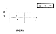
図13は誘導磁界52を検知して得られる信号波形図である。なお、この場合、磁気センサ素子4は図9を示し説明を行った同期整流方式の制御器40で制御された場合として説明を行う。そして、励振磁界51は交流であるが、同期整流方式であるため、向きを固定して説明を行うことができる。また、信号コイル2は、コイル面に直交する方向成分に反応する。そして、制御器40は、信号コイル2へ、下向きに磁界が入力すると負側に、上向きに磁界が入力すると正側に出力するように設定されているものとする。
図13及び上記の図12に示すとおり、磁性体53の通過に伴う制御器40から出力される信号波形は、ピーク点が、負側が現れてから正側が現れる単発の正弦波状となる。これは、信号コイル2で検出される信号強度は、信号コイル2に対する誘導磁界52の向きと大きさ、そして信号コイル2と磁性体53間の距離で決まることによる。信号コイル2に磁性体53が近づくに従い、信号コイル2に対して誘導磁界52は、下向き成分が次第に大きくなり、そして直上直前で下向き成分が最大となり、直上で水平となり、直上通過後に急激に上向き成分が大きくなり、ピークに至り、そして、遠ざかるに従い減衰してゆくことによる。
なお、この場合、移動の向きは、紙面を手前から見て左から右とした場合の誘導磁界52の変化を記載している。移動方向が反対の場合は、磁性体53の移動に伴う信号コイル2に入力される誘導磁界52の向きの変化が逆転するため、正弦波状の信号波形のピーク点は、正側が現れてから負側が現れる。
磁気センサ素子4を、図9を示し説明を行った制御器40で制御する場合、交流の励振磁界51を磁性体53に印加して同期整流方式で信号を処理するため、制御器40の高周波側の応答性能の範囲内であれば、信号波形の振幅は磁性体53の移動速度によらず一定となる。零速度を含みゆっくりとした移動であっても信号波形の振幅は変化しない。
FIG. 13 is a signal waveform diagram obtained by detecting the induced magnetic field 52. In this case, the magnetic sensor element 4 will be described as being controlled by the synchronous rectification type controller 40 described with reference to FIG. 9. The exciting magnetic field 51 is an alternating current, but since it is a synchronous rectification method, the direction can be fixed and the explanation can be given. Further, the signal coil 2 reacts to a directional component orthogonal to the coil surface. Then, it is assumed that the controller 40 is set to output to the negative side when a magnetic field is input downward and to the positive side when a magnetic field is input upward to the signal coil 2.
As shown in FIG. 13 and FIG. 12 above, the signal waveform output from the controller 40 accompanying the passage of the magnetic body 53 has a single sinusoidal shape in which the peak point appears on the negative side and then on the positive side. This is because the signal strength detected by the signal coil 2 is determined by the direction and magnitude of the induced magnetic field 52 with respect to the signal coil 2 and the distance between the signal coil 2 and the magnetic body 53. As the magnetic body 53 approaches the signal coil 2, the downward component of the induced magnetic field 52 gradually increases with respect to the signal coil 2, and the downward component becomes maximum immediately before the signal coil 2, becomes horizontal immediately above, and suddenly upwards after passing directly above. This is because the component grows, reaches its peak, and decays as it goes away.
In this case, the direction of movement describes the change in the induced magnetic field 52 when the paper surface is viewed from the front and is changed from left to right. When the moving directions are opposite, the change in the direction of the induced magnetic field 52 input to the signal coil 2 due to the movement of the magnetic body 53 is reversed, so that the peak point of the sinusoidal signal waveform becomes negative after the positive side appears. The side appears.
When the magnetic sensor element 4 is controlled by the controller 40 described with reference to FIG. 9, an alternating current excitation magnetic field 51 is applied to the magnetic body 53 to process a signal by a synchronous rectification method, so that the high frequency of the controller 40 is high. Within the range of the response performance on the side, the amplitude of the signal waveform is constant regardless of the moving speed of the magnetic material 53. The amplitude of the signal waveform does not change even if the movement is slow, including zero velocity.

図14は誘導磁界52の検出原理の別の概念図である。なお、図14は、励振電流50、励振磁界51及び誘導磁界52の向きはある瞬間におけるものとし、さらに磁気センサ素子4は固定されおり、円柱状の磁性体53がその底面を移動方向に向けて移動するものとして示している。
図14に示すとおり、本発明の磁気センサ素子の実施の形態3を備えた磁気センサ素子4を構成する励振コイル1の区画1wを流れる励振電流50は、励振電流50の流れる方向と直交する方向に励振磁界51を発生し、発生された励振磁界51は励振コイル1近傍に位置している磁性体53に印加される。磁性体53は、励振磁界51によって誘導磁界52を発生し、発生された誘導磁界52が信号コイル2に入力される。信号コイル2は、入力された誘導磁界52の内、コイル面に直交する方向成分の大きさ及び変化の速さに応じて電圧を発生させる。
FIG. 14 is another conceptual diagram of the detection principle of the induced magnetic field 52. In FIG. 14, the directions of the exciting current 50, the exciting magnetic field 51, and the induced magnetic field 52 are assumed to be at a certain moment, and the magnetic sensor element 4 is fixed, and the columnar magnetic body 53 directs the bottom surface in the moving direction. It is shown as moving.
As shown in FIG. 14, the excitation current 50 flowing through the compartment 1w of the excitation coil 1 constituting the magnetic sensor element 4 provided with the third embodiment of the magnetic sensor element of the present invention is in a direction orthogonal to the flow direction of the excitation current 50. The exciting magnetic field 51 is generated in the magnet, and the generated exciting magnetic field 51 is applied to the magnetic body 53 located near the excitation coil 1. The magnetic body 53 generates an induced magnetic field 52 by the exciting magnetic field 51, and the generated induced magnetic field 52 is input to the signal coil 2. The signal coil 2 generates a voltage in the input induced magnetic field 52 according to the magnitude of the directional component orthogonal to the coil surface and the speed of change.

図15は誘導磁界52を検知して得られる別の信号波形図である。なお、この場合、磁気センサ素子4は図9を示し説明を行った制御器40で制御された場合として説明を行う。そして、励振磁界51は交流であるが、同期整流方式であるため、向きを固定して説明を行うことができる。また、信号コイル2は、コイル面に直交する方向成分に反応する。そして、制御器40は、信号コイル2へ、紙面を手前から見て、右向きに磁界が入力すると負側に、左向きに磁界が入力すると正側に出力するように設定されているものとする。
図15及び上記の14に示すとおり、磁性体53の通過に伴う制御器40から出力される信号波形は山形で山の両脇に小さな窪みを持つ形となる。これは、信号コイル2で検出される信号強度は、信号コイル2に対する誘導磁界52の向きと大きさ、そして信号コイル2と磁性体53間の距離で決まることによる。信号コイル2に磁性体53が近づくに従い、信号コイル2に対しては、誘導磁界52は右向きに入り、次に、誘導磁界52は時計周りに回転し、左向きとなり、直上で、それが最大強度となり、直上通過後に、再び時計周りに回転することで、右向きに変わり、遠ざかるに従い減衰してゆくことによる。
磁気センサ素子4を、図9を示し説明を行った制御器40で制御する場合、交流の励振磁界51を磁性体53に印加して同期整流方式で信号を処理するため、制御器40の高周波側の応答性能の範囲内であれば、信号波形の振幅は磁性体53の移動速度によらず一定となる。零速度を含みゆっくりとした移動であっても信号波形の振幅は変化しない。
FIG. 15 is another signal waveform diagram obtained by detecting the induced magnetic field 52. In this case, the magnetic sensor element 4 will be described as if it were controlled by the controller 40 described in FIG. 9. The exciting magnetic field 51 is an alternating current, but since it is a synchronous rectification method, the direction can be fixed and the explanation can be given. Further, the signal coil 2 reacts to a directional component orthogonal to the coil surface. Then, it is assumed that the controller 40 is set to output to the signal coil 2 on the negative side when a magnetic field is input to the right and to the positive side when a magnetic field is input to the left when the paper surface is viewed from the front.
As shown in FIGS. 15 and 14 above, the signal waveform output from the controller 40 accompanying the passage of the magnetic body 53 is mountain-shaped and has small depressions on both sides of the mountain. This is because the signal strength detected by the signal coil 2 is determined by the direction and magnitude of the induced magnetic field 52 with respect to the signal coil 2 and the distance between the signal coil 2 and the magnetic body 53. As the magnetic material 53 approaches the signal coil 2, the induced magnetic field 52 enters the signal coil 2 to the right, then the induced magnetic field 52 rotates clockwise and turns to the left, which is directly above and has the maximum strength. By rotating clockwise again after passing directly above, it changes to the right and attenuates as it goes away.
When the magnetic sensor element 4 is controlled by the controller 40 described with reference to FIG. 9, an alternating current excitation magnetic field 51 is applied to the magnetic body 53 to process a signal by a synchronous rectification method, so that the high frequency of the controller 40 is high. Within the range of the response performance on the side, the amplitude of the signal waveform is constant regardless of the moving speed of the magnetic material 53. The amplitude of the signal waveform does not change even if the movement is slow, including zero velocity.

(本発明の磁気検出器の実施の形態1:1本のワイヤロープ検査用)
図16は1本のワイヤロープWの検査方法を説明する概念図である。
図16に示すとおり、この目的で使用する磁気検出器100は、ワイヤロープWの近傍において、ワイヤロープWに非接触状態として、壁などの構造物500に両面テープなどにより一時的に取り付けて使用される。ワイヤロープWはその軸方向において移動する。
(Embodiment 1: 1 for wire rope inspection of the magnetic detector of the present invention)
FIG. 16 is a conceptual diagram illustrating a method of inspecting one wire rope W.
As shown in FIG. 16, the magnetic detector 100 used for this purpose is used by temporarily attaching it to a structure 500 such as a wall with double-sided tape or the like in a non-contact state with the wire rope W in the vicinity of the wire rope W. Will be done. The wire rope W moves in its axial direction.

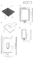
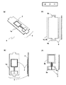
そして、図17(a)及び図17(b)は本発明の磁気検出器の実施の形態1を説明する斜視図である。これは図16で説明を行った磁気検出器100の実施の形態例として示す。ここで図17(a)は磁気検出器100の外観の斜視図、そして図17(b)は磁気検出器100の内部の斜視図である。図17(a)及び図17(b)に示すとおり、磁気検出器100は、ケース100c、電源供給及び信号の入出力を行う電線100d、本発明の磁気センサ素子の実施の形態1を備えた磁気センサ素子4及び図9を示し説明を行った制御器40を備える。ただし、磁気センサ素子4及び制御器40は、ガラス布基材エポキシ樹脂の基板10を共有して形成されている。制御器40を構成する基板10の上面側に取り付けられた電子部品は、基板10の上面側に形成された配線に半田付けすることで電気的に接続されている。
そして、磁気センサ素子4の励振コイル1の巻始め1sと巻終り1eと制御器40の励振部40cの間の電気的な接続は、基板10の上面側に形成された配線を介して行われている。さらに、信号コイル2の巻始め2sと巻終り2eと制御器40の交流増幅部40aの間の電気的な接続は、基板10の上面側に形成された信号コイル2の巻始め2sと巻終り2eに接続された配線、基板10の上面側の配線と下面側の配線を接続するめっきスルーホール、基板10の下面側の配線、基板10の下面側の配線と上面側の配線を接続するめっきスルーホール及び基板10の上面側の励振部40cに接続された配線によって行われている。
17 (a) and 17 (b) are perspective views illustrating the first embodiment of the magnetic detector of the present invention. This is shown as an example of the embodiment of the magnetic detector 100 described with reference to FIG. Here, FIG. 17A is a perspective view of the appearance of the magnetic detector 100, and FIG. 17B is a perspective view of the inside of the magnetic detector 100. As shown in FIGS. 17 (a) and 17 (b), the magnetic detector 100 includes a case 100c, an electric wire 100d for supplying power and inputting / outputting signals, and embodiment 1 of the magnetic sensor element of the present invention. The magnetic sensor element 4 and the controller 40 described with reference to FIG. 9 are provided. However, the magnetic sensor element 4 and the controller 40 are formed by sharing the substrate 10 of the glass cloth base material epoxy resin. The electronic components attached to the upper surface side of the substrate 10 constituting the controller 40 are electrically connected by soldering to the wiring formed on the upper surface side of the substrate 10.
Then, the electrical connection between the winding start 1s and winding end 1e of the excitation coil 1 of the magnetic sensor element 4 and the excitation portion 40c of the controller 40 is made via the wiring formed on the upper surface side of the substrate 10. ing. Further, the electrical connection between the winding start 2s and the winding end 2e of the signal coil 2 and the AC amplification unit 40a of the controller 40 is such that the winding start 2s and the winding end of the signal coil 2 formed on the upper surface side of the substrate 10 are connected. The wiring connected to 2e, the plating through hole that connects the wiring on the upper surface side and the wiring on the lower surface side of the substrate 10, the wiring on the lower surface side of the substrate 10, and the plating that connects the wiring on the lower surface side and the wiring on the upper surface side of the substrate 10. This is done by wiring connected to the through hole and the excitation portion 40c on the upper surface side of the substrate 10.

図18はワイヤロープWの素線断線54の検出原理の概念図である。なお、図18は、励振電流50、励振磁界51及び誘導磁界52の向きはある瞬間におけるものとし、さらに磁気検出器100は固定されており、ワイヤロープWが移動するものとして示している。
図18に示すとおり、本発明の磁気センサ素子の実施の形態1を備えた磁気センサ素子4を構成する励振コイル1の区画1wを流れる励振電流50は、励振電流50の流れる方向に直交する方向に励振磁界51を発生し、発生された励振磁界51は、励振コイル1近傍に位置しているワイヤロープWの側方からワイヤロープWの軸方向へワイヤロープWに対して印加される。ワイヤロープWの素線断線54箇所は励振磁界51によって誘導磁界52を発生し、発生した誘導磁界52が信号コイル2に入力される。信号コイル2は、入力された誘導磁界52の内、コイル面に直交する方向成分の大きさ及び変化の速さに応じた電圧を発生させる。
FIG. 18 is a conceptual diagram of the detection principle of the wire breakage 54 of the wire rope W. Note that FIG. 18 shows that the directions of the exciting current 50, the exciting magnetic field 51, and the induced magnetic field 52 are at a certain moment, the magnetic detector 100 is fixed, and the wire rope W moves.
As shown in FIG. 18, the excitation current 50 flowing through the compartment 1w of the excitation coil 1 constituting the magnetic sensor element 4 provided with the first embodiment of the magnetic sensor element of the present invention is in a direction orthogonal to the flow direction of the excitation current 50. The exciting magnetic field 51 is generated in the above direction, and the generated exciting magnetic field 51 is applied to the wire rope W from the side of the wire rope W located in the vicinity of the excitation coil 1 in the axial direction of the wire rope W. An induced magnetic field 52 is generated by the exciting magnetic field 51 at 54 locations where the wire rope W is disconnected, and the generated induced magnetic field 52 is input to the signal coil 2. The signal coil 2 generates a voltage in the input induced magnetic field 52 according to the magnitude of the directional component orthogonal to the coil surface and the speed of change.

図19はワイヤロープWの素線断線54から得られる信号波形図である。なお、この場合、磁気センサ素子4は図9を示し説明を行った制御器40で制御された場合として説明を行う。そして、励振磁界51は交流であるが、同期整流方式であるため、向きを固定して説明を行うことができる。また、信号コイル2は、コイル面に直交する方向成分に反応する。そして、制御器40は、この信号コイルへ、下向きに磁界が入力すると負側に、上向きに磁界が入力すると正側に出力するように設定されているものとする。
図19及び上記の図18に示すとおり、ワイヤロープWの素線断線54の通過に伴う制御器40から出力される信号波形は、ピーク点が、正側が現れてから負側が現れる単発の正弦波状となる。これは、信号コイル2で検出される信号強度は、信号コイル2に対する誘導磁界52の向きと大きさ、そして信号コイル2とワイヤロープWの素線断線54間の距離で決まることによる。信号コイル2にワイヤロープWの素線断線54が近づくに従い、信号コイル2に対して誘導磁界52は、上向き成分が次第に大きくなり、そして直上直前で、上向き成分が最大となり、直上で水平となり、直上通過後に急激に下向き成分が大きくなり、ピークに至り、そして、遠ざかるに従い減衰してゆくことによる。
なお、この場合、移動の向きは、紙面を手前から見て左から右とした場合の誘導磁界52の変化を記載している。移動方向が反対の場合は、ワイヤロープWの素線断線54の移動に伴う信号コイル2に入力される誘導磁界52の向きの変化が逆転するため、正弦波状の信号波形のピーク点は、負側が現れてから正側が現れる。
FIG. 19 is a signal waveform diagram obtained from the wire disconnection 54 of the wire rope W. In this case, the magnetic sensor element 4 will be described as if it were controlled by the controller 40 described in FIG. 9. The exciting magnetic field 51 is an alternating current, but since it is a synchronous rectification method, the direction can be fixed and the explanation can be given. Further, the signal coil 2 reacts to a directional component orthogonal to the coil surface. Then, it is assumed that the controller 40 is set to output to the negative side when a magnetic field is input downward and to the positive side when a magnetic field is input upward to the signal coil.
As shown in FIG. 19 and FIG. 18 above, the signal waveform output from the controller 40 due to the passage of the wire rope disconnection 54 is a single sinusoidal shape in which the peak point appears on the positive side and then appears on the negative side. It becomes. This is because the signal strength detected by the signal coil 2 is determined by the direction and magnitude of the induced magnetic field 52 with respect to the signal coil 2 and the distance between the signal coil 2 and the wire rope disconnection 54 of the wire rope W. As the wire rope disconnection 54 of the wire rope W approaches the signal coil 2, the inductive magnetic field 52 gradually increases in the upward component with respect to the signal coil 2, and immediately before the signal coil 2, the upward component becomes maximum and becomes horizontal immediately above. This is because the downward component suddenly increases after passing directly above, reaches a peak, and then attenuates as it goes away.
In this case, the direction of movement describes the change in the induced magnetic field 52 when the paper surface is viewed from the front and is changed from left to right. When the moving directions are opposite, the change in the direction of the induced magnetic field 52 input to the signal coil 2 due to the movement of the wire break 54 of the wire rope W is reversed, so that the peak point of the sinusoidal signal waveform is negative. The positive side appears after the side appears.

磁気センサ素子4を、図9を示し説明を行った制御器40で制御する場合、交流の励振磁界51をワイヤロープWに印加して同期整流方式で信号を処理するため、高感度な磁気検出器100が得られる。さらに、制御器40の高周波数側の応答性能の範囲内であれば、信号波形の振幅はワイヤロープWの移動速度によらず一定となり、零速度を含みゆっくりとした移動であっても信号波形の振幅は変化しないという特徴を持つことができる。
また、ワイヤロープWを含み磁性体53は、内部の磁化の大きさ及び向きが揃っていないことを原因として、磁性体53の損傷の検出に雑音として影響を与え、磁性体53の検査の障害となる場合がある。こういった場合は、あらかじめ磁石あるいは電磁石により磁性体53に磁界を印加して磁性体53の磁化の大きさ及び向きを整えて、その後に磁気検出器100で磁性体53の損傷の検査を行うと良い。図19で示した信号波形の基線の揺らぎは、ワイヤロープWの内部の磁化の大きさ及び向きの不揃いに起因した成分が含まれている。
When the magnetic sensor element 4 is controlled by the controller 40 shown and described in FIG. 9, the AC excitation magnetic field 51 is applied to the wire rope W to process the signal by the synchronous rectification method, so that the magnetic detection is highly sensitive. The vessel 100 is obtained. Further, within the range of the response performance on the high frequency side of the controller 40, the amplitude of the signal waveform becomes constant regardless of the moving speed of the wire rope W, and the signal waveform includes a zero speed even if the movement is slow. Can have the characteristic that the amplitude of is unchanged.
Further, the magnetic body 53 including the wire rope W affects the detection of damage of the magnetic body 53 as noise due to the fact that the magnitudes and directions of the magnetizations inside the magnetic body 53 are not uniform, and the inspection of the magnetic body 53 is hindered. May be. In such a case, a magnetic field is applied to the magnetic body 53 in advance by a magnet or an electromagnet to adjust the magnitude and direction of the magnetization of the magnetic body 53, and then the magnetic detector 100 inspects the magnetic body 53 for damage. Is good. The fluctuation of the baseline of the signal waveform shown in FIG. 19 contains a component due to the irregularity of the magnitude and direction of the magnetization inside the wire rope W.

(本発明の磁気センサ素子の実施の形態5:2本のワイヤロープW同時かつ個別検査用)
図20は本発明の磁気センサ素子の実施の形態5を説明する斜視図である。この形態は、2本のワイヤロープWを同時かつ個別に検査可能である。なお、図20では基板10を省略しているが、以下では、基板10を含めた説明を行う。
図20に示すとおり、本発明の磁気センサ素子の実施の形態5を備える磁気センサ素子4は、ガラス布基材エポキシ樹脂から形成された基板10と、基板10の下面側で銅箔から形成された励振コイル1と、複数の信号コイル2とを備える。励振コイル1は、その区画1wが複数個の信号コイル2を形成できる大きさで形成されている。複数個の信号コイル2は、信号コイル2_3、信号コイル2_4、信号コイル2_1、信号コイル2_2、信号コイル2_1h及び信号コイル2_2hからなり、信号コイル2_3と信号コイル2_4は、図2を示し説明を行った本発明の磁気センサ素子の実施の形態2と同様にして形成されている。また、信号コイル2_1、信号コイル2_2、信号コイル2_1h及び信号コイル2_2hは、図3を示し説明を行った本発明の磁気センサ素子の実施の形態3と同様にして形成されている。
信号コイル2_1、信号コイル2_2、信号コイル2_1h及び信号コイル2_2hは、それぞれのコイル面を励振磁界51の方向に向けており、励振磁界51を直接検出するため、ワイヤロープWの素線断線54からの微小な信号を検出できない状態にある。このため、信号コイル2_1、信号コイル2_2、信号コイル2_1h及び信号コイル2_2hは、信号コイル2_1と信号コル2_1h、そして、信号コイル2_2と信号コイル2_2hという組み合わせで、それぞれ、後述する差動コイル7を形成する。図20に示す例では、信号コイル2_1hと信号コイル2_2hが励振磁界51の影響を除去するための補償用でワイヤロープWが通過するところから離れたところに形成されている。
そして、信号コイル2_1と信号コイル2_3が1本のワイヤロープWの直下に、信号コイル2_2と信号コイル2_4が別の1本のワイヤロープWの直下になるように形成されている。
上記の結果、信号コイル2_3と信号コイル2_4は、ワイヤロープWから発生される誘導磁界52の内、区画1wの面に直交する方向の誘導磁界52を検出できる。このため、得られる信号波形は、ワイヤロープWの損傷の直下で信号が零となるが損傷付近で信号が大きく早く変化する形を持つ。信号コイル2_3及び信号コイル2_4は素線断線54のような局所的な損傷の検出に向く。また、信号コイル2_1と信号コイル2_2は、ワイヤロープWから発生される誘導磁界52の内、区画1wの面に平行な成分を検出できる。このため、得られる信号波形は、ワイヤロープWの損傷の直下で振幅が最大となる。信号コイル2_1と信号コイル2_2はワイヤロープWの損傷の内、摩耗、内部断線あるいは錆によるワイヤロープWの径の変化など素線断線54に比べると範囲を持った損傷、さらに加えて、ワイヤロープWの緩み、異常振動などの異変の検出にも向く。
なお、上記の例はワイヤロープW2本用であるが、同様にワイヤロープW3本以上用として励振コイル1と複数個の信号コイル2とは、積層を形成しても良い。
(Embodiment 5 of the magnetic sensor element of the present invention: two wire ropes W for simultaneous and individual inspection)
FIG. 20 is a perspective view illustrating the fifth embodiment of the magnetic sensor element of the present invention. In this form, two wire ropes W can be inspected simultaneously and individually. Although the substrate 10 is omitted in FIG. 20, the description including the substrate 10 will be described below.
As shown in FIG. 20, the magnetic sensor element 4 according to the fifth embodiment of the magnetic sensor element of the present invention is formed of a substrate 10 formed of a glass cloth base material epoxy resin and a copper foil on the lower surface side of the substrate 10. The excitation coil 1 and a plurality of signal coils 2 are provided. The excitation coil 1 is formed in such a size that the compartment 1w can form a plurality of signal coils 2. The plurality of signal coils 2 are composed of signal coil 2_3, signal coil 2_4, signal coil 2_1, signal coil 2_2, signal coil 2_1h and signal coil 2_2h, and the signal coil 2_3 and the signal coil 2_2 are described with reference to FIG. It is formed in the same manner as in the second embodiment of the magnetic sensor element of the present invention. Further, the signal coil 2_1, the signal coil 2_2, the signal coil 2_1h, and the signal coil 2_2h are formed in the same manner as in the third embodiment of the magnetic sensor element of the present invention shown and described in FIG.
The signal coil 2_1, the signal coil 2_2, the signal coil 2_1h, and the signal coil 2_2h have their respective coil surfaces directed in the direction of the exciting magnetic field 51, and in order to directly detect the exciting magnetic field 51, the wire rope W is connected from the wire disconnection 54. It is in a state where it cannot detect a minute signal. Therefore, the signal coil 2_1, the signal coil 2_2, the signal coil 2_1h, and the signal coil 2_2h are a combination of the signal coil 2_1 and the signal coil 2_1h, and the signal coil 2_2 and the signal coil 2_2h, respectively. Form. In the example shown in FIG. 20, the signal coil 2_1h and the signal coil 2_2h are formed at a position away from the place where the wire rope W passes for compensation for removing the influence of the exciting magnetic field 51.
The signal coil 2_1 and the signal coil 2___ are formed so as to be directly under one wire rope W, and the signal coil 2_2 and the signal coil 2___ are formed so as to be directly under another wire rope W.
As a result of the above, the signal coil 2_3 and the signal coil 2_4 can detect the induced magnetic field 52 in the direction orthogonal to the plane of the compartment 1w among the induced magnetic fields 52 generated from the wire rope W. Therefore, the obtained signal waveform has a form in which the signal becomes zero immediately below the damage of the wire rope W, but the signal changes significantly and quickly in the vicinity of the damage. The signal coil 2_3 and the signal coil 2_4 are suitable for detecting local damage such as a wire break 54. Further, the signal coil 2_1 and the signal coil 2_2 can detect a component parallel to the surface of the compartment 1w in the induced magnetic field 52 generated from the wire rope W. Therefore, the obtained signal waveform has the maximum amplitude immediately below the damage of the wire rope W. The signal coil 2_1 and the signal coil 2_1 have a wider range of damage than the wire rope 54, such as wear, internal disconnection, or change in the diameter of the wire rope W due to rust, among the damages of the wire rope W. In addition, the wire rope It is also suitable for detecting abnormalities such as loosening of W and abnormal vibration.
Although the above example is for two wire ropes W, similarly, the excitation coil 1 and the plurality of signal coils 2 may be laminated for three or more wire ropes W.

(本発明の磁気センサ素子の実施の形態6:差動コイル7)
図21は本発明の磁気センサ素子の実施の形態6を説明する斜視図である。この形態は、差動コイル7と称され、2つの信号コイル2を持ち、第1の縦巻き信号コイルでありながら、励振磁界51を直接検出せずに、測定対象物からの微小な信号を検出できる。なお、図21では基板10を省略しているが、以下では、基板10を含めた説明を行う。
図21に示すとおり、本発明の磁気センサ素子の実施の形態6を備える磁気センサ素子4は、ガラス布基材エポキシ樹脂から形成された基板10と、基板10の下面側で銅箔から形成された励振コイル1と、基板10の上側で銅箔から形成された2個の信号コイル2とを備える。2つの信号コイル2は信号コイル2_1と信号コイル2_1hからなり、本発明の磁気センサ素子の実施の形態4の信号コイル2と同様にして形成されている。信号コイル2_1の巻終り2eと信号コイル2_1hの巻終り2eが配線で電気的に接続され、信号コイル2_1の巻始め2sが差動コイル7の巻終り7eに配線で電気的に接続され、信号コイル2_1hの巻始め2sが差動コイル7の巻始め7sに配線で電気的に接続されている。
配線に関しては、図21に示すように、信号コイル2_1の巻終り2eと信号コイル2_1hの巻終り2eを、差動コイル7の巻始め7s及び巻終り7eが形成された層とは別な層の銅箔とめっきスルーホールを利用して接続することで、電線など外部からの配線を使用することなく、差動コイル7の巻始め7sと巻終り7eを同じ層において形成している。
そして、信号コイル2_1と信号コイル2_1hは、同じ形状寸法で、コイル面を励振磁界51に対して同じ方向を向け、略同じ大きさの励振磁界51を検出するところである区画1wの面に直交する方向から見て区画1wの中央付近に形成されている。
さらに加えて、信号コイル2_1は、検査対象とするワイヤロープWの直下となるように、信号コイル2_1hは、検査対象とするワイヤロープWから離れたところに形成される。信号コイル2_1hが、励振磁界51の補償用として使用される。
なお、差動コイル7に電流を流すと、差動コイル7を形成する信号コイル2_1と信号コイル2_hにおいて流れる電流の向きが逆となる。そして、これが差動コイルと称される所以である。
(Embodiment 6: Differential Coil 7 of the Magnetic Sensor Element of the Present Invention)
FIG. 21 is a perspective view illustrating embodiment 6 of the magnetic sensor element of the present invention. This form is called a differential coil 7, has two signal coils 2, and although it is the first vertically wound signal coil, it does not directly detect the exciting magnetic field 51, but receives a minute signal from the object to be measured. Can be detected. Although the substrate 10 is omitted in FIG. 21, the description including the substrate 10 will be described below.
As shown in FIG. 21, the magnetic sensor element 4 according to the sixth embodiment of the magnetic sensor element of the present invention is formed of a substrate 10 formed of a glass cloth base material epoxy resin and a copper foil on the lower surface side of the substrate 10. The excitation coil 1 and the two signal coils 2 formed of copper foil on the upper side of the substrate 10 are provided. The two signal coils 2 are composed of a signal coil 2_1 and a signal coil 2_1h, and are formed in the same manner as the signal coil 2 of the fourth embodiment of the magnetic sensor element of the present invention. The winding end 2e of the signal coil 2_1 and the winding end 2e of the signal coil 2_1h are electrically connected by wiring, and the winding start 2s of the signal coil 2_1 is electrically connected to the winding end 7e of the differential coil 7 by wiring, and the signal is signaled. The winding start 2s of the coil 2_1h is electrically connected to the winding start 7s of the differential coil 7 by wiring.
Regarding the wiring, as shown in FIG. 21, the winding end 2e of the signal coil 2_1 and the winding end 2e of the signal coil 2_1h are different from the layer on which the winding start 7s and the winding end 7e of the differential coil 7 are formed. By connecting to the copper foil of the above using a plated through hole, the winding start 7s and the winding end 7e of the differential coil 7 are formed in the same layer without using external wiring such as an electric wire.
The signal coil 2_1 and the signal coil 2_1h have the same shape and dimensions, face the coil surface in the same direction with respect to the exciting magnetic field 51, and are orthogonal to the surface of the compartment 1w where the exciting magnetic field 51 of substantially the same size is detected. It is formed near the center of the compartment 1w when viewed from the direction.
Furthermore, the signal coil 2_1h is formed at a position away from the wire rope W to be inspected so that the signal coil 2_1 is directly below the wire rope W to be inspected. The signal coil 2_1h is used for compensating the exciting magnetic field 51.
When a current is passed through the differential coil 7, the directions of the currents flowing through the signal coil 2_1 and the signal coil 2_h forming the differential coil 7 are opposite to each other. And this is the reason why it is called a differential coil.

(本発明の磁気センサ素子の実施の形態7:複数本ワイヤロープ一括検査用)
図22(a)〜図22(e)は本発明の磁気センサ素子の実施の形態7を説明する図である。これを用いれば、複数本のワイヤロープWを一括で検査することが可能である。ここで、図22(a)は磁気センサ素子4の斜視図、図22(b)は励振コイル1と信号コイル2の斜視図、図22(c)は励振コイル1と信号コイル2の正面図と側面図、図22(d)は励振コイル1の正面図と側面図そして図22(e)は信号コイル2の正面図と側面図である。
図22(a)〜図22(e)に示すように、磁気センサ素子4は、ガラス布基材エポキシ樹脂から形成された基板10と、基板10の下面側において銅箔から形成された励振コイル1と、基板10の上面側において銅箔から形成された信号コイル2と、を備える。励振コイル1は、励振コイル1に印加される励振電流50の流れる方向に直交する方向において幅の広い銅箔からなる区画1wを含んで形成される。信号コイル2は、区画1wの面に直交する方向から見て、略区画1w内に形成されている。
そして、励振コイル1は、図22(d)に示すとおり、巻始め1s、コイル本体1b及び巻終り1eという構成により1回平巻きコイルとして形成される。信号コイル2は、図22(e)に示すとおり、巻始め2s、本体2b及び巻終り2eという構成により2回平巻きコイルとして形成される。
なお、区画1wの面に直交する方向から見て、区画1wを超えて形成された信号コイル2の巻終り2eは、その直下に、励振コイル1を形成する銅箔層がないため、励振コイル1が形成された層を利用した配線がしやすい。また、区画1wの面に直交する方向から見て区画1wを超えて形成された信号コイル2の部分については、ワイヤロープWから離れるように形成すれば、ワイヤロープWからの信号の検出に対する関与の割合を下げることができるため、複数本のワイヤロープWのそれぞれの損傷に対して、同じ程度の損傷であれば、同じ程度の信号が得られようになる。
また、図23は3本のワイヤロープWの検査方法を説明する斜視図である。3本のワイヤロープWを一括で検査する方法として示す。図22を示し説明を行った本発明の磁気センサ素子の実施の形態7を備えた磁気センサ素子4を用いる。3本のワイヤロープWは、基板10に対して平行に、細長い信号コイル2の横手方向に軸方向をそろえ、信号コイル2の長手方向に対して中央付近に設置されている。そして、3本のワイヤロープWは、3本同時にあるいはそれぞれに、その軸方向に移動する。
この例の磁気検出器100としては、複数本のワイヤロープWの内、少なくとも1本のワイヤロープWに損傷があるとそれを検知して、外部に結果を出力するような機能性能を持つものを提供することが可能となる。この形態は、ワイヤロープWの緩み、異常振動など異変の検出に向く。
(Embodiment 7 of the magnetic sensor element of the present invention: for batch inspection of a plurality of wire ropes)
22 (a) to 22 (e) are views for explaining the seventh embodiment of the magnetic sensor element of the present invention. By using this, it is possible to inspect a plurality of wire ropes W at once. Here, FIG. 22A is a perspective view of the magnetic sensor element 4, FIG. 22B is a perspective view of the excitation coil 1 and the signal coil 2, and FIG. 22C is a front view of the excitation coil 1 and the signal coil 2. 22 (d) is a front view and a side view of the excitation coil 1, and FIG. 22 (e) is a front view and a side view of the signal coil 2.
As shown in FIGS. 22 (a) to 22 (e), the magnetic sensor element 4 is a substrate 10 formed of a glass cloth base material epoxy resin and an excitation coil formed of a copper foil on the lower surface side of the substrate 10. 1 and a signal coil 2 formed of copper foil on the upper surface side of the substrate 10 are provided. The excitation coil 1 is formed including a compartment 1w made of a copper foil having a wide width in a direction orthogonal to the flow direction of the excitation current 50 applied to the excitation coil 1. The signal coil 2 is formed in the substantially compartment 1w when viewed from a direction orthogonal to the plane of the compartment 1w.
Then, as shown in FIG. 22D, the excitation coil 1 is formed as a one-time flat winding coil by a configuration of a winding start 1s, a coil body 1b, and a winding end 1e. As shown in FIG. 22 (e), the signal coil 2 is formed as a two-fold flat winding coil by a configuration of a winding start 2s, a main body 2b, and a winding end 2e.
When viewed from the direction orthogonal to the plane of the compartment 1w, the winding end 2e of the signal coil 2 formed beyond the compartment 1w does not have a copper foil layer forming the excitation coil 1 immediately below the winding end 2e of the signal coil 2. Wiring using the layer on which 1 is formed is easy. Further, if the portion of the signal coil 2 formed beyond the compartment 1w when viewed from the direction orthogonal to the plane of the compartment 1w is formed so as to be separated from the wire rope W, it is involved in the detection of the signal from the wire rope W. Therefore, for each damage of the plurality of wire ropes W, if the damage is the same, the same signal can be obtained.
Further, FIG. 23 is a perspective view illustrating an inspection method of the three wire ropes W. It is shown as a method of inspecting three wire ropes W at once. The magnetic sensor element 4 provided with the seventh embodiment of the magnetic sensor element of the present invention described with reference to FIG. 22 is used. The three wire ropes W are arranged parallel to the substrate 10 in the axial direction in the lateral direction of the elongated signal coil 2 and near the center in the longitudinal direction of the signal coil 2. Then, the three wire ropes W move in the axial direction of the three wire ropes W simultaneously or individually.
The magnetic detector 100 of this example has a functional performance of detecting damage to at least one wire rope W among a plurality of wire ropes W and outputting the result to the outside. Can be provided. This form is suitable for detecting abnormalities such as loose wire rope W and abnormal vibration.

(様々な分野での磁気センサ素子の利用例)
上記では、本発明に係る磁気センサ素子及びそれを用いた磁気検出器を、ワイヤロープ検査用として説明を行ったが、本発明に係る磁気センサ素子は、様々な分野において広く利用できる。以下で説明を行う。
(Examples of use of magnetic sensor elements in various fields)
In the above, the magnetic sensor element according to the present invention and the magnetic detector using the same have been described for wire rope inspection, but the magnetic sensor element according to the present invention can be widely used in various fields. This will be described below.

(非磁性導体の検出について)
磁性体53から発生する誘導磁界52の検出原理は、図12及び図13を示し説明を行ったとおりであるが、本発明に係る磁気センサ素子を用いた磁気検出器100は、磁性体53から発生される誘導磁界52の他に、非磁性導体60から発生される渦電流磁界62についても検出可能である。
図24は渦電流磁界62の検出原理を説明する概念図である。なお、図24は、励振電流50、励振磁界51、渦電流61、渦電流磁界62の向きはある瞬間におけるものとし、さらに磁気センサ素子4は固定されており、円柱状の非磁性導体60がその底面を移動方向に向けて移動するものとして示している。
図24に示すとおり、本発明の磁気センサ素子の実施の形態1を備えた磁気センサ素子4を構成する励振コイル1の区画1wを流れる励振電流50は、励振電流50の流れる方向と直交する方向に励振磁界51を発生し、発生された励振磁界51は励振コイル1近傍に位置している非磁性導体60に印加される。この時、非磁性導体60中には、励振磁界51の入力を妨げるように渦電流磁界62を発生させる渦電流61が流れる。そして、発生した渦電流磁界62が信号コイル2に入力される。信号コイル2は、入力された渦電流磁界62の内、コイル面に直交する方向成分の大きさ及び変化の速さに応じて電圧を発生させる。
(About detection of non-magnetic conductors)
The detection principle of the induced magnetic field 52 generated from the magnetic body 53 is as described with reference to FIGS. 12 and 13, but the magnetic detector 100 using the magnetic sensor element according to the present invention is described from the magnetic body 53. In addition to the induced magnetic field 52 generated, the eddy current magnetic field 62 generated from the non-magnetic conductor 60 can also be detected.
FIG. 24 is a conceptual diagram illustrating the detection principle of the eddy current magnetic field 62. In FIG. 24, the directions of the exciting current 50, the exciting magnetic field 51, the eddy current 61, and the eddy current magnetic field 62 are assumed to be at a certain moment, and the magnetic sensor element 4 is fixed, and the columnar non-magnetic conductor 60 is formed. The bottom surface is shown as moving in the moving direction.
As shown in FIG. 24, the excitation current 50 flowing through the compartment 1w of the excitation coil 1 constituting the magnetic sensor element 4 provided with the first embodiment of the magnetic sensor element of the present invention is in a direction orthogonal to the flow direction of the excitation current 50. The exciting magnetic field 51 is generated in, and the generated exciting magnetic field 51 is applied to the non-magnetic conductor 60 located in the vicinity of the exciting coil 1. At this time, an eddy current 61 that generates an eddy current magnetic field 62 flows through the non-magnetic conductor 60 so as to obstruct the input of the exciting magnetic field 51. Then, the generated eddy current magnetic field 62 is input to the signal coil 2. The signal coil 2 generates a voltage in the input eddy current magnetic field 62 according to the magnitude of the directional component orthogonal to the coil surface and the speed of change.

図25は渦電流磁界62を検知して得られる信号波形図である。なお、この場合、磁気センサ素子4は図9を示し説明を行った制御器40で制御された場合として説明を行う。そして、励振磁界51は交流であるが、同期整流方式であるため、向きを固定して説明を行うことができる。また、信号コイル2は、コイル面に直交する方向成分に反応する。そして、制御器40は、信号コイル2へ、下向きに磁界が入力すると負側に、上向きに磁界が入力すると正側に出力するように設定されているものとする。
図25及び上記の図24に示すとおり、非磁性導体60の通過に伴う制御器40から出力される信号波形は、ピーク点が、正側が現れてから負側が現れる単発の正弦波状となる。これは、信号コイル2で検出される信号強度は、信号コイル2に対する渦電流磁界62の向きと大きさそして非磁性導体60と信号コイル2間の距離で決まることによる。信号コイル2に非磁性導体60が近づくに従い、信号コイル2に対して渦電流磁界62は、上向き成分が次第に大きくなり、そして直上直前で上向き成分が最大となり、直上で水平となり、直上通過後に急激に下向き成分が大きくなり、ピークに至り、そして、遠ざかるに従い減衰してゆくことによる。
なお、この場合、移動の向きは、紙面を手前から見て左から右とした場合の渦電流磁界62の変化を記載している。移動方向が反対の場合は、非磁性導体60の移動に伴う信号コイル2に入力される渦電流磁界62の向きの変化が逆転するため、正弦波状の信号波形のピーク点は、負側が現れてから正側が現れる。
磁気センサ素子4を、図9を示し説明を行った制御器40で制御する場合、交流の励振磁界51を非磁性導体60に印加して同期整流方式で信号を処理するため、制御器40の高周波側の応答性能の範囲内であれば信号波形の振幅は非磁性導体60の移動速度によらず一定となる。零速度を含みゆっくりとした移動であっても信号波形の振幅は変化しない。
FIG. 25 is a signal waveform diagram obtained by detecting the eddy current magnetic field 62. In this case, the magnetic sensor element 4 will be described as if it were controlled by the controller 40 described in FIG. 9. The exciting magnetic field 51 is an alternating current, but since it is a synchronous rectification method, the direction can be fixed and the explanation can be given. Further, the signal coil 2 reacts to a directional component orthogonal to the coil surface. Then, it is assumed that the controller 40 is set to output to the negative side when a magnetic field is input downward and to the positive side when a magnetic field is input upward to the signal coil 2.
As shown in FIG. 25 and FIG. 24 above, the signal waveform output from the controller 40 accompanying the passage of the non-magnetic conductor 60 has a single sinusoidal shape in which the peak point appears on the positive side and then on the negative side. This is because the signal strength detected by the signal coil 2 is determined by the direction and magnitude of the eddy current magnetic field 62 with respect to the signal coil 2 and the distance between the non-magnetic conductor 60 and the signal coil 2. As the non-magnetic conductor 60 approaches the signal coil 2, the eddy current magnetic field 62 gradually increases in the upward component with respect to the signal coil 2, and the upward component becomes maximum immediately before the signal coil 2, becomes horizontal immediately above, and suddenly after passing directly above. This is because the downward component becomes larger, reaches a peak, and then attenuates as it goes away.
In this case, the direction of movement describes the change in the eddy current magnetic field 62 when the paper surface is viewed from the front from the left to the right. When the moving directions are opposite, the change in the direction of the eddy current magnetic field 62 input to the signal coil 2 due to the movement of the non-magnetic conductor 60 is reversed, so that the peak point of the sinusoidal signal waveform appears on the negative side. The positive side appears from.
When the magnetic sensor element 4 is controlled by the controller 40 described with reference to FIG. 9, the AC excitation magnetic field 51 is applied to the non-magnetic conductor 60 to process the signal by the synchronous rectification method. Within the range of the response performance on the high frequency side, the amplitude of the signal waveform is constant regardless of the moving speed of the non-magnetic conductor 60. The amplitude of the signal waveform does not change even if the movement is slow, including zero velocity.

(回転測定:磁気検出器を有する装置の実施の形態1)
図26(a)〜図26(c)は磁気検出器を有する装置の実施の形態1を説明する斜視図である。モータ、エンコーダなど回転軸を有する装置111の回転軸の回転検出用として示す。図26(a)〜図26(c)に示すとおり、装置111は、本発明の磁気センサ素子の実施の形態1を備えた磁気検出器100と、回転軸200、ハウジング210などを有し、磁気検出器100は、回転軸200の近傍において、ハウジング210に固定して使用される。そして、回転軸200は、磁気検出器100を構成する磁気センサ素子4の信号コイル2の近傍に設置され、さらに、少なくとも回転軸200の信号コイル2近傍に位置する部分には、磁性体53あるいは非磁性導体60が使用され、さらに回転軸200の回転に伴い、信号コイル2に入力される誘導磁界52あるいは渦電流磁界62が変化するような特徴を持たせている。例えば、回転軸200の信号コイル2の近傍に位置する部分は、突起201、溝202、歯車203とするなど形状を変化させる。これによって、回転軸200の回転に伴い、励振磁界51によって発生する誘導磁界52あるいは渦電流磁界62の信号コイル2に入力する成分の大きさと向きが変化する。したがって、磁気検出器100の出力をモニターすることで、回転軸200の回転速度、回転数あるいは回転角度を知ることができる。
なお、本発明に係る磁気検出器の場合、図12及び図13を示し説明を行ったとおり、移動の向きによって得られる単発の正弦波状の信号波形が異なるため、あらかじめ回転軸200の回転方向と信号波形の関係を求めておけば、その信号波形から、回転方向を知ることができる。
(Rotation measurement: Embodiment 1 of an apparatus having a magnetic detector)
26 (a) to 26 (c) are perspective views illustrating the first embodiment of an apparatus having a magnetic detector. It is shown for detecting the rotation of the rotating shaft of a device 111 having a rotating shaft such as a motor or an encoder. As shown in FIGS. 26 (a) to 26 (c), the device 111 includes a magnetic detector 100 including the first embodiment of the magnetic sensor element of the present invention, a rotating shaft 200, a housing 210, and the like. The magnetic detector 100 is used by being fixed to the housing 210 in the vicinity of the rotating shaft 200. The rotating shaft 200 is installed in the vicinity of the signal coil 2 of the magnetic sensor element 4 constituting the magnetic detector 100, and further, a magnetic material 53 or a magnetic material 53 or a portion located near the signal coil 2 of the rotating shaft 200 is provided. The non-magnetic conductor 60 is used, and further has a feature that the induced magnetic field 52 or the eddy current magnetic field 62 input to the signal coil 2 changes with the rotation of the rotating shaft 200. For example, the portion of the rotating shaft 200 located near the signal coil 2 is changed in shape such as a protrusion 201, a groove 202, and a gear 203. As a result, as the rotating shaft 200 rotates, the size and direction of the components input to the signal coil 2 of the induced magnetic field 52 or the eddy current magnetic field 62 generated by the exciting magnetic field 51 change. Therefore, by monitoring the output of the magnetic detector 100, it is possible to know the rotation speed, the rotation speed, or the rotation angle of the rotation shaft 200.
In the case of the magnetic detector according to the present invention, as described with reference to FIGS. 12 and 13, the single-shot sinusoidal signal waveform obtained differs depending on the direction of movement. If the relationship between the signal waveforms is obtained, the rotation direction can be known from the signal waveform.

(変位測定:磁気検出器を有する装置の実施の形態2)
図27は磁気検出器を有する装置の実施の形態2を説明する斜視図である。変位計測用として示す。図27に示すとおり、装置111は、本発明の磁気センサ素子の実施の形態1を備えた磁気検出器100と、測定対象物に接触させる部品である接触子302と、接触子302に連動する連動子303と、連動子303を磁気検出器100の近傍で保持するホルダー304と、磁性体53あるいは非磁性導体60からなる被検出子305と、を備え、被検出子305は、磁気検出器100を構成する信号コイル2と同程度以下の大きさとされて連動子303に固定されており、連動子303は、接触子302の動きと連動するようにホルダー304で保持されていることを特徴とする。
これによって、被検出子305の移動に伴い、励振磁界51によって被検出子305から発生する誘導磁界52あるいは渦電流磁界62の信号コイル2に入力する成分の大きさと向きが変化する。あらかじめ接触子302の変位量と磁気検出器100の出力の関係を求めておけば、磁気検出器100の出力から接触子302の変位量を知ることができる。
(Displacement measurement: Embodiment 2 of an apparatus having a magnetic detector)
FIG. 27 is a perspective view illustrating a second embodiment of an apparatus having a magnetic detector. Shown for displacement measurement. As shown in FIG. 27, the device 111 is interlocked with the magnetic detector 100 provided with the first embodiment of the magnetic sensor element of the present invention, the contact 302 which is a component to be brought into contact with the object to be measured, and the contact 302. The interlocking element 303, the holder 304 holding the interlocking element 303 in the vicinity of the magnetic detector 100, and the detector 305 made of a magnetic body 53 or a non-magnetic conductor 60 are provided, and the detector 305 is a magnetic detector. The size of the interlocking coil 2 is about the same as or smaller than that of the signal coil 2 constituting the 100, and the interlocking element 303 is fixed to the interlocking element 303. And.
As a result, as the detector 305 moves, the magnitude and direction of the components input to the signal coil 2 of the induction magnetic field 52 or the eddy current magnetic field 62 generated from the detector 305 by the excitation magnetic field 51 change. If the relationship between the displacement amount of the contactor 302 and the output of the magnetic detector 100 is obtained in advance, the displacement amount of the contactor 302 can be known from the output of the magnetic detector 100.

(磁気探傷:磁気検出器の利用例)
鋼材の磁気探傷用として、図17を示し説明を行った本発明の磁気検出器の実施の形態1を備えた磁気検出器100が利用可能である。この場合、制御器40の電子部品が搭載された面とは反対側の面、つまり磁気検出器100として平たい方の面を測定対象物に向けて移動させるような使い方をする。
検出原理は、図18を示し説明を行ったワイヤロープWの素線断線54から発生する誘導磁界52を検出するのと同じ原理による。測定対象物が、ワイヤロープWから棒状の鋼材あるいは平板状の鋼材に代わり、ワイヤロープWの素線断線54が鋼材の傷に代わるということになる。
磁気検出器100として、構成に磁石あるいは電磁石を使用しないため、軽量化、小型化が可能である。また、フレキシブルプリント配線板を使用して、本発明に係る磁気センサ素子を形成するならば、測定対象物は、平板に限定されず、筒状のものであっても探傷を行うことができる。
なお、探傷すべき傷の形状と磁気検出器100の走査方向との関係によって、得られる信号の大きさが変化するような場合は、励振磁界51を直交する2方向からそれぞれに印加できるように励振コイル1を2系統設けるなど工夫をすると良い。また、信号コイル2は、第1の平巻き信号コイル、第1の縦巻き信号コイルあるいはそれらを複合させたものなど、種々の形態で用いても良い。さらに、励振コイル1に印加する励振電流50の周波数を可変として磁気検出器100を構築し、励振周波数との関係で、磁気検出器100の出力を解析することで鋼材の傷の深さについても情報が得られるようになる。
以下では、ここで説明を行った磁気検出器100を本発明に係る磁気探傷器と称する。
(Magnetic flaw detection: Example of using magnetic detector)
For magnetic flaw detection of steel materials, the magnetic detector 100 provided with the first embodiment of the magnetic detector of the present invention described with reference to FIG. 17 can be used. In this case, the surface of the controller 40 opposite to the surface on which the electronic components are mounted, that is, the flat surface of the magnetic detector 100 is moved toward the object to be measured.
The detection principle is based on the same principle as that for detecting the induced magnetic field 52 generated from the wire disconnection 54 of the wire rope W described with reference to FIG. The object to be measured changes from the wire rope W to the rod-shaped steel material or the flat plate-shaped steel material, and the wire disconnection 54 of the wire rope W replaces the scratches on the steel material.
Since the magnetic detector 100 does not use a magnet or an electromagnet in its configuration, it can be made lighter and smaller. Further, if the magnetic sensor element according to the present invention is formed by using the flexible printed wiring board, the object to be measured is not limited to a flat plate, and even a tubular object can be used for flaw detection.
If the magnitude of the obtained signal changes depending on the relationship between the shape of the scratch to be detected and the scanning direction of the magnetic detector 100, the exciting magnetic field 51 can be applied to each of the two orthogonal directions. It is advisable to devise such as providing two excitation coils 1. Further, the signal coil 2 may be used in various forms such as a first flat-wound signal coil, a first vertical-wound signal coil, or a combination thereof. Further, the magnetic detector 100 is constructed by making the frequency of the excitation current 50 applied to the excitation coil 1 variable, and the output of the magnetic detector 100 is analyzed in relation to the excitation frequency to obtain the depth of scratches on the steel material. Information will be available.
Hereinafter, the magnetic detector 100 described here will be referred to as a magnetic flaw detector according to the present invention.

(渦電流探傷:磁気検出器の利用例)
アルミニウムなど非磁性導体60の探傷用としても、図17を示し説明を行った本発明の磁気検出器の実施の形態1を備えた磁気検出器100が利用可能である。この場合も、制御器40の電子部品が搭載された面とは反対側の面、つまり磁気検出器100の平たい方の面を測定対象物に向けて移動させるような使い方をする。
検出原理は、図24及び図25を示し説明を行ったように非磁性導体60が発生する渦電流磁界62を検出するのと同様の原理による。なお、測定対象物が非磁性導体60の平板である場合は、この平板に励振磁界51が印加されると、この平板中に、励振磁界51の変化を妨げるような渦電流磁界62を発生させる渦電流61が流れる。この際に、この平板中に傷があれば、これによって渦電流61の流れが乱れ、これが渦電流磁界62の変化となり、磁気検出器100によって検出される。
フレキシブルプリント配線板を使用して、本発明に係る磁気センサ素子を形成するならば、測定対象物は、平板に限定されず、筒状のものであっても探傷を行うことができる。
なお、本発明に係る磁気検出器の場合、測定対象物の傷から発生される信号波形が、誘導磁界52によるものか渦電流磁界62によるものかは、信号波形から判定することが可能である。渦電流磁界62は、測定対象物に励振磁界51が印加され、その変化を妨げるように発生するものであるため、傷の形状が同じであればその単発の正弦波状の信号波形の上側ピークと下側ピークの現れる順番が誘導磁界52の場合とは逆の関係になる。
以下では、ここで説明を行った磁気検出器100を本発明に係る渦電流探傷器と称する。
(Eddy current flaw detection: Example of using magnetic detector)
Also for flaw detection of a non-magnetic conductor 60 such as aluminum, the magnetic detector 100 provided with the first embodiment of the magnetic detector of the present invention shown and described in FIG. 17 can be used. Also in this case, the surface opposite to the surface on which the electronic component of the controller 40 is mounted, that is, the flat surface of the magnetic detector 100 is moved toward the measurement object.
The detection principle is the same as that for detecting the eddy current magnetic field 62 generated by the non-magnetic conductor 60 as described with reference to FIGS. 24 and 25. When the object to be measured is a flat plate of the non-magnetic conductor 60, when the exciting magnetic field 51 is applied to the flat plate, an eddy current magnetic field 62 that hinders the change of the exciting magnetic field 51 is generated in the flat plate. An eddy current 61 flows. At this time, if there is a scratch in the flat plate, the flow of the eddy current 61 is disturbed by this, which changes the eddy current magnetic field 62, which is detected by the magnetic detector 100.
If the magnetic sensor element according to the present invention is formed by using the flexible printed wiring board, the object to be measured is not limited to a flat plate, and even a tubular object can be used for flaw detection.
In the case of the magnetic detector according to the present invention, it is possible to determine from the signal waveform whether the signal waveform generated from the scratch on the object to be measured is due to the induced magnetic field 52 or the eddy current magnetic field 62. .. Since the eddy current magnetic field 62 is generated so as to prevent the change of the exciting magnetic field 51 when the excitation magnetic field 51 is applied to the object to be measured, if the shape of the scratch is the same, the eddy current magnetic field 62 will be the upper peak of the single sinusoidal signal waveform. The order in which the lower peaks appear is opposite to that in the case of the induced magnetic field 52.
Hereinafter, the magnetic detector 100 described here will be referred to as an eddy current flaw detector according to the present invention.

(食品異物検出:磁気検出器の利用例)
食品異物検出用としても、図17を示し説明を行った本発明の磁気検出器の実施の形態1を備えた磁気検出器100が利用可能である。
異物として検出可能なものは、磁性体53及び非磁性導体60の両方である。基本とする原理は、図12及び図13並びに図24及び図25を示し説明を行ったところと同様である。
なお、食品異物検査装置全体が、装置111に相当する。
(Food foreign matter detection: Example of using magnetic detector)
Also for food foreign matter detection, the magnetic detector 100 provided with the first embodiment of the magnetic detector of the present invention described with reference to FIG. 17 can be used.
What can be detected as foreign matter is both the magnetic material 53 and the non-magnetic conductor 60. The basic principle is the same as that shown and described in FIGS. 12 and 13, and FIGS. 24 and 25.
The entire food foreign matter inspection device corresponds to the device 111.

(硬貨識別:磁気検出器の利用例)
硬貨識別用としても、図17を示し説明を行った本発明の磁気検出器の実施の形態1を備えた磁気検出器100が利用可能である。
この場合、磁気検出器100には、磁気検出器100の近くを硬貨が移動するように構成したガイド部品を組み合わせる。
硬貨は、導体60であるため、検出に渦電流磁界62が利用できる。磁気検出器100を構成する信号コイル2の形状寸法と硬貨の形状寸法材質との関係で、磁気検出器100の出力変化が定まる。あらかじめ各種硬貨と磁気検出器100で得られる出力信号の関係を求めておくことで硬貨識別を行う。
なお、ガイド部品の寸法精度により、硬貨のガイド部品を通過する場所が一定せず、識別能力が劣化する場合は、磁気検出器100を2個使用し、ガイド部品の両側に配置して、硬貨識別を行うと劣化が緩和される。ただし、この場合、2つの磁気検出器100が近接して配置されるため、対策を講じないと、相互干渉による雑音が発生し硬貨識別能力がかえって劣化する。この対策としては、2つある磁気検出器100に内蔵された励振コイル1に対して同じ励振電流50を印加するか、あるいは制御器40の入出力部40eを利用し2つの磁気検出器100間で通信を行い、励振を時分割で行うあるいは同時に行うなど同期をとりながら動作させると良い。
(Coin identification: Example of using magnetic detector)
Also for coin identification, the magnetic detector 100 provided with the first embodiment of the magnetic detector of the present invention described with reference to FIG. 17 can be used.
In this case, the magnetic detector 100 is combined with a guide component configured so that the coin moves near the magnetic detector 100.
Since the coin is a conductor 60, an eddy current magnetic field 62 can be used for detection. The output change of the magnetic detector 100 is determined by the relationship between the shape dimension of the signal coil 2 constituting the magnetic detector 100 and the shape dimension material of the coin. Coins are identified by obtaining the relationship between various coins and the output signal obtained by the magnetic detector 100 in advance.
If the location through which the guide part of the coin passes is not constant due to the dimensional accuracy of the guide part and the discrimination ability deteriorates, use two magnetic detectors 100 and arrange them on both sides of the guide part to place the coin. Deterioration is mitigated by identification. However, in this case, since the two magnetic detectors 100 are arranged close to each other, noise due to mutual interference is generated and the coin identification ability is rather deteriorated unless countermeasures are taken. As a countermeasure, the same excitation current 50 is applied to the excitation coil 1 built in the two magnetic detectors 100, or the input / output unit 40e of the controller 40 is used between the two magnetic detectors 100. It is good to operate while synchronizing by communicating with and exciting by time division or at the same time.

(近接検出:磁気検出器を有する装置の実施の形態3)
図28は磁気検出器を有する装置の実施の形態3を説明する斜視図である。近接検出用として示す。図28に示すとおり、装置111は、本発明の磁気検出器の実施の形態1を備えた磁気検出器100と、軟磁性材102と、被検出体311と、を備え、軟磁性材102は、磁気検出器100のケースに接着して取り付けられている。軟磁性材102の取り付け位置は、励振コイル1の区画1wの面に直交する方向から信号コイル2を見て、信号コイル2を覆う位置である。なお、軟磁性材102の例としてはパーマロイ、被検出体の例としては磁石がある。
検出原理は、被検出体311の接近にともない、被検出体311が発生する磁界により、この軟磁性材102の磁気的な性質が変化することを利用することによる。つまり、この軟磁性材102の磁気的な変化によって、励振磁界51により発生する誘導磁界52の向きと大きさが変化する。そして、この変化は信号コイル2から出力される信号電圧の変化となる。
あらかじめ、被検出体311と軟磁性材102を取り付けた磁気検出器100間の距離と、軟磁性材102を取り付けた磁気検出器100の出力との関係を求めておくと、その信号の大きさから被検出体の接近距離を知ることができる。
(Proximity detection: Embodiment 3 of an apparatus having a magnetic detector)
FIG. 28 is a perspective view illustrating the third embodiment of the device having a magnetic detector. Shown for proximity detection. As shown in FIG. 28, the apparatus 111 includes a magnetic detector 100 provided with the first embodiment of the magnetic detector of the present invention, a soft magnetic material 102, and an object to be detected 311. , Adhered to the case of the magnetic detector 100. The mounting position of the soft magnetic material 102 is a position that covers the signal coil 2 when the signal coil 2 is viewed from a direction orthogonal to the surface of the section 1w of the excitation coil 1. An example of the soft magnetic material 102 is permalloy, and an example of the object to be detected is a magnet.
The detection principle is based on the fact that the magnetic properties of the soft magnetic material 102 change due to the magnetic field generated by the detected body 311 as the detected body 311 approaches. That is, the direction and magnitude of the induced magnetic field 52 generated by the exciting magnetic field 51 change due to the magnetic change of the soft magnetic material 102. Then, this change becomes a change in the signal voltage output from the signal coil 2.
If the relationship between the distance between the detector 311 and the magnetic detector 100 to which the soft magnetic material 102 is attached and the output of the magnetic detector 100 to which the soft magnetic material 102 is attached is obtained in advance, the magnitude of the signal is obtained. The approach distance of the detected object can be known from.

(地磁気計測:本発明の磁気検出器の実施の形態2及び本発明の磁気センサ素子の実施の形態8)
図29(a)〜図29(c)は本発明の磁気検出器の実施の形態2を説明する斜視図である。地磁気計測用として示す。ここで図29(a)は磁気検出器100の外観の斜視図、図29(b)はその内部の斜視図、図29(c)は軟磁性材102を除いた内部の斜視図である。
また、図30は本発明の磁気センサ素子の実施の形態8を説明する斜視図である。これは図29で示す磁気検出器100において使用されるものとして示す。
図29(a)〜図29(c)及び図30に示すように、磁気検出器100は、軟磁性材102と、磁気センサ素子4と、制御器40と、ケース40cと、ケーブル100dを備えている。磁気センサ素子4と制御器40は基板10を共有している。
磁気センサ素子4は、励振コイル1と本発明の磁気センサ素子の実施の形態4を持つ第1の縦巻き信号コイルである信号コイル2_1と信号コイル2_2から形成され、励振コイル1は、区画1w_1及び区画1w_2を有し、区画1w_1と区画1w_2を流れる励振電流50が互いに逆向きになるようにコイル路が形成されている。なお、励振電流50が互いに逆向きになることについては、図30にある瞬間における電流の流れる向きを描いたとおりである。信号コイル2_1は、区画1w_1の面に直交する方向から見て区画1w_1内に形成され、信号コイル2_2は、区画1w_2の面に直交する方向から見て、区画1w_2内に形成されている。さらに、信号コイル2_2の巻終り2eと信号コイル2_1の巻始め2sが接続されている。これにより、信号コイル2_1と信号コイル2_2の各々が検出する励振磁界51は打ち消される。したがって、この2つの信号コイル2_1と信号コイル2_2を合わせた信号つまり信号コイル2_2の巻始め2sと信号コイル2_1の巻終り2e間に発生する信号電圧からは、励振磁界51の直接的な影響が除去される。
軟磁性材102は、励振コイル1の区画1w_1あるいは1w_2の面に直交する方向から見て、2つの第1の縦巻き信号コイルを覆うようにして磁気センサ素子4に接着されている。なお、基板10はガラス布基材エポキシ樹脂、励振コイル1は銅箔、受信コイル2は銅箔、軟磁性材102はパーマロイで形成されているものとする。なお、軟磁性材102は2つの第1の縦巻き信号コイルを個別に覆うように構成しても良い。また、磁気センサ素子4の両面に設けてもよい。
以下で、外部から入力される磁界を地磁気として、検出原理を説明する。磁気検出器100において、基板10に平行に、磁気検出器100の横手方向から地磁気が入力すると、軟磁性材102には、励振磁界51と地磁気が入力される。励振磁界51は2つの第1の縦巻き信号コイルにおいて、向きが互いに逆となるように形成されている。ある瞬間においては、一方の第1の縦巻き信号コイルの近傍に位置している軟磁性材102部分には、励振磁界51と地磁気が加算されて入力し、別の一方の軟磁性材102部分には、励振磁界51から地磁気が減算されて入力する。軟磁性材102は、そのB−H特性に従い磁気飽和する特性を持つ。したがって、地磁気の入力によって、一方の軟磁性材102部分が飽和領域にあり、別の一方の軟磁性材102部分が飽和領域に至らない状態となる時間領域が発生する。つまり、地磁気の入力がない場合、各々の第1の縦巻き信号コイルにおいて励振磁界51により発生している信号電圧は一致するが、地磁気の入力があると、これが一致しない時間領域が発生する。したがって、2つの第1の縦巻き信号コイルを接続した端末から出力される信号は、入力する地磁気の大きさに応じて変化する。これが検出原理である。
あらかじめ、入力する地磁気の大きさと磁気検出器100の出力との関係を求めておけば、磁気検出器100の出力から地磁気の大きさを知ることができる。
なお、第1の縦巻き信号コイルは、その面の向く方向を、1方向のみで形成するのではなく、直交する2方向に向けて第1の縦巻き信号コイルを用いて形成すれば、直交2軸で地磁気を計測でき、方位計として利用が可能となる。
(Geomagnetic measurement: Embodiment 2 of the magnetic detector of the present invention and Embodiment 8 of the magnetic sensor element of the present invention)
29 (a) to 29 (c) are perspective views illustrating the second embodiment of the magnetic detector of the present invention. Shown for geomagnetic measurement. Here, FIG. 29A is a perspective view of the appearance of the magnetic detector 100, FIG. 29B is a perspective view of the inside thereof, and FIG. 29C is a perspective view of the inside excluding the soft magnetic material 102.
Further, FIG. 30 is a perspective view illustrating the eighth embodiment of the magnetic sensor element of the present invention. This is shown as being used in the magnetic detector 100 shown in FIG.
As shown in FIGS. 29 (a) to 29 (c) and 30, the magnetic detector 100 includes a soft magnetic material 102, a magnetic sensor element 4, a controller 40, a case 40c, and a cable 100d. ing. The magnetic sensor element 4 and the controller 40 share a substrate 10.
The magnetic sensor element 4 is formed of an excitation coil 1, a signal coil 2_1 and a signal coil 2_2, which are first vertically wound signal coils having the fourth embodiment of the magnetic sensor element of the present invention, and the excitation coil 1 is a compartment 1w_1. The coil path is formed so that the excitation current 50 flowing through the compartment 1w_1 and the compartment 1w_2 is opposite to each other. The fact that the excitation currents 50 are opposite to each other is as shown in FIG. 30 as the direction in which the current flows at the moment. The signal coil 2_1 is formed in the compartment 1w_1 when viewed from a direction orthogonal to the plane of the compartment 1w_1, and the signal coil 2_1 is formed in the compartment 1w_1 when viewed from a direction orthogonal to the plane of the compartment 1w_2. Further, the winding end 2e of the signal coil 2_2 and the winding start 2s of the signal coil 2_1 are connected. As a result, the exciting magnetic field 51 detected by each of the signal coil 2_1 and the signal coil 2_2 is canceled. Therefore, the signal voltage generated between the winding start 2s of the signal coil 2_1 and the winding end 2e of the signal coil 2_1, which is a combination of the two signal coils 2_1 and the signal coil 2_2, has a direct effect of the exciting magnetic field 51. Will be removed.
The soft magnetic material 102 is adhered to the magnetic sensor element 4 so as to cover the two first vertically wound signal coils when viewed from a direction orthogonal to the plane of the section 1w_1 or 1w_2 of the excitation coil 1. It is assumed that the substrate 10 is made of a glass cloth base epoxy resin, the excitation coil 1 is made of copper foil, the receiving coil 2 is made of copper foil, and the soft magnetic material 102 is made of permalloy. The soft magnetic material 102 may be configured to individually cover the two first vertically wound signal coils. Further, it may be provided on both sides of the magnetic sensor element 4.
In the following, the detection principle will be described using the magnetic field input from the outside as the geomagnetism. In the magnetic detector 100, when the geomagnetism is input from the lateral direction of the magnetic detector 100 in parallel with the substrate 10, the exciting magnetic field 51 and the geomagnetism are input to the soft magnetic material 102. The exciting magnetic field 51 is formed in the two first vertically wound signal coils so that the directions are opposite to each other. At a certain moment, the exciting magnetic field 51 and the geomagnetism are added and input to the soft magnetic material 102 portion located in the vicinity of one first vertically wound signal coil, and the other soft magnetic material 102 portion is input. Is input by subtracting the geomagnetism from the exciting magnetic field 51. The soft magnetic material 102 has a property of magnetically saturating according to its BH characteristics. Therefore, due to the input of the geomagnetism, a time region is generated in which one soft magnetic material 102 portion is in the saturation region and the other soft magnetic material 102 portion does not reach the saturation region. That is, when there is no geomagnetic input, the signal voltages generated by the exciting magnetic field 51 in each of the first vertically wound signal coils match, but when there is a geomagnetic input, a time domain in which they do not match occurs. Therefore, the signal output from the terminal to which the two first vertically wound signal coils are connected changes according to the magnitude of the input geomagnetism. This is the detection principle.
If the relationship between the magnitude of the geomagnetism to be input and the output of the magnetic detector 100 is obtained in advance, the magnitude of the geomagnetism can be known from the output of the magnetic detector 100.
It should be noted that the first vertically wound signal coil is orthogonal if it is formed by using the first vertically wound signal coil in two orthogonal directions instead of forming the direction in which the surface faces in only one direction. The geomagnetism can be measured with two axes, and it can be used as an azimuth meter.

(応力検出1:磁気検出器の利用例)
応力検出の分野で使用可能な磁気検出器100としては、図17を示し説明を行った本発明の磁気検出器の実施の形態1において、磁気センサ素子4を、図3を示し説明を行った本発明の磁気センサ素子の実施の形態3に変更した磁気検出器100が使用可能である。
応力検出は、磁性体53が応力の印加に応じてその磁性を変化させることを利用する。例えば、測定対象物が、自動車のタイヤに直結した磁性体53の車軸であれば、ねじりトルクを知ることができる。これは、磁気検出器100を、ワイヤロープWの損傷を測定したのと同じような状態で、磁気検出器100をこの車軸に接近させて設置し動作させることで行う。つまりこの状態は、図17で示すワイヤロープWを車軸に置き換えた状態を言う。あらかじめ、測定対象物である車軸に印加されるねじりトルクの大きさと磁気検出器100の出力の関係を求めておけば、磁気検出器100の出力から印加されているねじりトルクの大きさが分かる。
応力検出に関しては、この他に、鉄あるいは鉄合金の残留応力の分布の測定、それに基づく疲労度あるいは応力印加の履歴の推定などへの利用が可能である。また、測定結果を記録しておき、最新の記録と比較検討することにより、劣化の進行についての情報も得られる。
なお、測定対象物の形状は、棒状のものに限らず、平板状、筒状のものであっても良い。測定対象物への適合は、磁気センサ素子4の形成の仕方で対応すると良い。例えば、測定対象物が筒状であれば、磁気センサ素子4を、フレキシブルプリント配線板を使って形成すると良い。
(Stress detection 1: Usage example of magnetic detector)
As the magnetic detector 100 that can be used in the field of stress detection, the magnetic sensor element 4 is shown and described in FIG. 3 in the first embodiment of the magnetic detector of the present invention which has been described by showing FIG. The magnetic detector 100 modified to the third embodiment of the magnetic sensor element of the present invention can be used.
The stress detection utilizes the fact that the magnetic body 53 changes its magnetism in response to the application of stress. For example, if the object to be measured is the axle of the magnetic body 53 directly connected to the tire of an automobile, the torsional torque can be known. This is performed by installing and operating the magnetic detector 100 in a state similar to that for measuring the damage of the wire rope W, with the magnetic detector 100 close to the axle. That is, this state means a state in which the wire rope W shown in FIG. 17 is replaced with an axle. If the relationship between the magnitude of the torsional torque applied to the axle, which is the object to be measured, and the output of the magnetic detector 100 is obtained in advance, the magnitude of the torsional torque applied from the output of the magnetic detector 100 can be known.
In addition to this, stress detection can be used for measuring the distribution of residual stress in iron or iron alloys, and estimating the degree of fatigue or the history of stress application based on the distribution. In addition, by recording the measurement results and comparing them with the latest records, information on the progress of deterioration can be obtained.
The shape of the object to be measured is not limited to a rod shape, but may be a flat plate shape or a tubular shape. The compatibility with the object to be measured may be adjusted by the method of forming the magnetic sensor element 4. For example, if the object to be measured is tubular, the magnetic sensor element 4 may be formed by using a flexible printed wiring board.

(応力検出2:本発明の磁気センサ素子の実施の形態9及び磁気検出器を有する装置の実施の形態4)
応力検出の分野で使用可能な別の磁気センサ素子4としては、本発明の磁気センサ素子の実施の形態1において、基板10の材質をガラス布基材エポキシ樹脂から鉄合金などの磁性体に変更し、信号コイル2を複数個分布させて形成したものを利用することができる。この形態を本発明の磁気センサ素子の実施の形態9と称する。
または、フレキシブルプリント配線板を用いて磁気センサ素子4を形成し、磁性体53に接着する方法で形成しても良い。
図31は磁気検出器を有する装置の実施の形態4を説明する斜視図である。衝突検出用として示す。図31に示すとおり、装置111は、本発明の磁気センサ素子の実施の形態9を備えた磁気センサ素子4と制御器40からなる磁気検出器100と、自動車400本体とから構成され、磁気検出器100は自動車400の前面の下の方に取り付けられ、制御器40は磁気センサ素子4を同期整流方式で制御し、複数個の信号コイル2からの信号を受信できるように多チャンネル化されている。
物体が、磁気センサ素子4に衝突すると、磁性体53の基板10には応力が印加されその磁性を変化さる。この時に、励振磁界51により磁性体53の基板10から発生している誘導磁界52が変化し、この変化が信号コイル2に入力され、信号コイル2からは信号電圧の変化となって現れる。これが検出原理である。そして、この信号電圧の変化が制御器40で処理されて出力される。装置111としては、この出力された信号をもとに、例えば、この出力があるレベルを超えたならば、エアバックを開くなど異常に対する処理を行う。磁性体である基板10が塑性変形に至るより以前に検出できるため、衝突を早期に検出できることが特徴である。
(Stress detection 2: Embodiment 9 of the magnetic sensor element of the present invention and embodiment 4 of the device having a magnetic detector)
As another magnetic sensor element 4 that can be used in the field of stress detection, in the first embodiment of the magnetic sensor element of the present invention, the material of the substrate 10 is changed from a glass cloth base epoxy resin to a magnetic material such as an iron alloy. However, a plurality of signal coils 2 formed by distributing them can be used. This embodiment is referred to as a ninth embodiment of the magnetic sensor element of the present invention.
Alternatively, the magnetic sensor element 4 may be formed by using a flexible printed wiring board and may be formed by adhering to the magnetic body 53.
FIG. 31 is a perspective view illustrating the fourth embodiment of the device having a magnetic detector. Shown for collision detection. As shown in FIG. 31, the device 111 includes a magnetic detector 100 including a magnetic sensor element 4 and a controller 40 according to the ninth embodiment of the magnetic sensor element of the present invention, and an automobile 400 main body, and magnetic detection is performed. The device 100 is attached to the lower part of the front surface of the automobile 400, and the controller 40 controls the magnetic sensor element 4 by a synchronous rectification method and is multi-channel so that signals from a plurality of signal coils 2 can be received. There is.
When an object collides with the magnetic sensor element 4, stress is applied to the substrate 10 of the magnetic body 53 to change its magnetism. At this time, the induction magnetic field 52 generated from the substrate 10 of the magnetic body 53 changes due to the exciting magnetic field 51, and this change is input to the signal coil 2 and appears as a change in the signal voltage from the signal coil 2. This is the detection principle. Then, this change in signal voltage is processed by the controller 40 and output. Based on this output signal, the device 111 performs processing for an abnormality such as opening an airbag when the output exceeds a certain level. Since the substrate 10 which is a magnetic material can be detected before it reaches plastic deformation, it is characterized in that collision can be detected at an early stage.

(応力検出3:本発明の磁気センサ素子の実施の形態10)
図32(a)〜図32(d)は本発明の磁気センサ素子の実施の形態10を説明する図である。探傷用として示す。ここで、図32(a)は磁気センサ素子4の斜視図、図32(b)は磁気センサ素子4の正面図と側面図、図32(c)は励振コイル1の正面図と側面図、図32(d)は信号コイル2の正面図と側面図である。図32(a)〜図32(d)に示すとおり、磁気センサ4は、ばね性を持つ非磁性導体であるリン青銅から形成された励振コイル1と、励振コイル1の上側でリン青銅から形成された信号コイル2とを備える。信号コイル2と励振コイル1とは、接着剤9で接着することで積層を形成している。励振コイル1は、励振コイル1に印加される励振電流50の流れる方向に直交する方向において幅の広いリン青銅からなる区画1wを含んで形成される。信号コイル2の本体2bは、区画1wの面に直交する方向から見て区画1wの中央付近において区画1w内に形成される。
そして、励振コイル1は、図32(c)に示すとおり、巻始め1s、コイル本体1b及び巻終り1eという構成により1回平巻きコイルとして形成される。信号コイル2は、図32(d)に示すとおり、巻始め2s、本体2b及び巻終り2eという構成により1回平巻きコイルとして形成される。信号コイル2の巻始め2s及び巻終り2eは、リード線を半田付けしやすいように大きな面積を持たせている。
この形態の特徴は取扱性が向上することである。これは、磁気探傷あるいは渦電流探傷の分野において、検査対象物に磁気センサ素子4を密着させて移動する際に、励振コイル2を形成しているリン青銅のばね性を利用できることによる。このばね性により、検査対象物に密着させるための力加減の許容範囲が広がり、操作が容易になる。なお、励振コイルの本体2b内の溝については、例えば、励振コイル1と信号コイル2とは、積層を形成する際に使用する接着材で埋めるようにすると良い。また、その際に使用する接着材は、弾性を有するものを使用すると良い。
(本発明の磁気センサ素子の実施の形態11:第2の信号コイルの例)
(Stress Detection 3: Embodiment 10 of the magnetic sensor element of the present invention)
32 (a) to 32 (d) are views for explaining the tenth embodiment of the magnetic sensor element of the present invention. Shown for flaw detection. Here, FIG. 32 (a) is a perspective view of the magnetic sensor element 4, FIG. 32 (b) is a front view and a side view of the magnetic sensor element 4, and FIG. 32 (c) is a front view and a side view of the excitation coil 1. FIG. 32 (d) is a front view and a side view of the signal coil 2. As shown in FIGS. 32 (a) to 32 (d), the magnetic sensor 4 is formed of an excitation coil 1 formed of phosphor bronze, which is a non-magnetic conductor having a spring property, and a phosphor bronze on the upper side of the excitation coil 1. The signal coil 2 is provided. The signal coil 2 and the excitation coil 1 are laminated with an adhesive 9. The excitation coil 1 is formed including a compartment 1w made of phosphor bronze having a wide width in a direction orthogonal to the flow direction of the excitation current 50 applied to the excitation coil 1. The main body 2b of the signal coil 2 is formed in the compartment 1w near the center of the compartment 1w when viewed from a direction orthogonal to the plane of the compartment 1w.
Then, as shown in FIG. 32 (c), the excitation coil 1 is formed as a one-time flat winding coil by a configuration of a winding start 1s, a coil body 1b, and a winding end 1e. As shown in FIG. 32 (d), the signal coil 2 is formed as a one-time flat winding coil by a configuration of a winding start 2s, a main body 2b, and a winding end 2e. The winding start 2s and winding end 2e of the signal coil 2 have a large area so that the lead wire can be easily soldered.
The feature of this form is that the handleability is improved. This is because, in the field of magnetic flaw detection or eddy current flaw detection, the spring property of phosphor bronze forming the excitation coil 2 can be utilized when the magnetic sensor element 4 is brought into close contact with the inspection object and moved. Due to this springiness, the allowable range of force adjustment for adhering to the inspection object is widened, and the operation becomes easy. Regarding the groove in the main body 2b of the excitation coil, for example, the excitation coil 1 and the signal coil 2 may be filled with an adhesive used when forming a laminate. Further, the adhesive used at that time may be an adhesive having elasticity.
(Embodiment 11 of the magnetic sensor element of the present invention: Example of a second signal coil)

図33(a)〜図33(e)は、本発明の磁気センサ素子の実施の形態11を説明する図である。ここで、図33(a)は磁気センサ素子4の斜視図、図33(b)は励振コイル1と信号コイル3の斜視図、図33(c)は励振コイル1と信号コイル3の正面図と側面図、図33(d)は励振コイル1の正面図と側面図、図33(e)は信号コイル3の正面図と側面図である。
図33(a)〜図33(e)に示すように、磁気センサ素子4は、ガラス布基材エポキシ樹脂から形成された基板10と、基板10の下面側において銅箔から形成された励振コイル1と、基板10の上面側において銅箔から形成された信号コイル3(第2の信号コイルに相当する)とを備える。励振コイル1は、励振電流50の流れる向きが互いに逆となる銅箔からなる区画1w_1及び銅箔からなる区画1w_2と、境界5と、を有し、境界5は、区画1w_1と区画1w_2とが互いに隣接することで形成され、信号コイル3が、区画1w_1あるいは1w_2の面に直交する方向から見て、境界5を含み、境界5を除いては境界5を形成する区画1w_1と区画1w_2とを合わせた区画内に形成される。
そして、励振コイル1は、図33(d)に示すとおり、巻始め1s、コイル本体1b及び巻終り1eという構成により1回平巻きコイルとして形成される。信号コイル3は、図33(e)に示すとおり、巻始め3s、本体3b及び巻終り3eという構成により1回平巻きコイルとして形成される。
なお、ここで説明を行った信号コイル3については、第2の平巻き信号コイルと称する。
33 (a) to 33 (e) are views for explaining the eleventh embodiment of the magnetic sensor element of the present invention. Here, FIG. 33A is a perspective view of the magnetic sensor element 4, FIG. 33B is a perspective view of the excitation coil 1 and the signal coil 3, and FIG. 33C is a front view of the excitation coil 1 and the signal coil 3. 33 (d) is a front view and a side view of the excitation coil 1, and FIG. 33 (e) is a front view and a side view of the signal coil 3.
As shown in FIGS. 33 (a) to 33 (e), the magnetic sensor element 4 is a substrate 10 formed of a glass cloth base material epoxy resin and an excitation coil formed of a copper foil on the lower surface side of the substrate 10. 1 and a signal coil 3 (corresponding to a second signal coil) formed of copper foil on the upper surface side of the substrate 10 are provided. The excitation coil 1 has a section 1w_1 made of copper foil in which the directions in which the excitation current 50 flows are opposite to each other, a section 1w_1 made of copper foil, and a boundary 5, and the boundary 5 has a section 1w_1 and a section 1w_2. A section 1w_1 and a section 1w_2 formed by being adjacent to each other and formed by a signal coil 3 including a boundary 5 and forming a boundary 5 except for the boundary 5 when viewed from a direction orthogonal to the plane of the section 1w_1 or 1w_2. It is formed in the combined compartment.
Then, as shown in FIG. 33 (d), the excitation coil 1 is formed as a one-time flat winding coil by a configuration of a winding start 1s, a coil body 1b, and a winding end 1e. As shown in FIG. 33 (e), the signal coil 3 is formed as a one-time flat winding coil by a configuration of a winding start 3s, a main body 3b, and a winding end 3e.
The signal coil 3 described here is referred to as a second flat-wound signal coil.

図34はワイヤロープWの素線断線54の検出原理の別の概念図である。本発明の磁気センサ素子の実施の形態11を備えた磁気センサ素子4を用いる場合として示す。なお、図34は、励振電流50_1と50_2、励振磁界51_1と51_2及び誘導磁界52gの向きはある瞬間におけるものとし、さらに磁気センサ素子4は固定されており、ワイヤロープWが移動するものとして示している。
図34に示すとおり、励振電流50_1は励振磁界51_1を、励振電流50_2は、励振磁界51_2を、その流れる方向と直交する方向に発生し、発生した励振磁界51_1及び励振磁界51_2が、励振コイル1近傍に位置しているワイヤロープWの側方からワイヤロープWの軸方向へワイヤロープWに対して印加される。ワイヤロープWの素線断線54箇所は、励振磁界51_1と励振磁界51_2の合成した励振磁界によって誘導磁界52gを発生し、発生した誘導磁界52gが信号コイル2に入力される。信号コイル2は、入力された誘導磁界52gの内、コイル面に直交する方向成分の大きさ及び変化の速さに応じた電圧を発生させる。
FIG. 34 is another conceptual diagram of the detection principle of the wire breakage 54 of the wire rope W. The case where the magnetic sensor element 4 provided with the eleventh embodiment of the magnetic sensor element of the present invention is used is shown. In FIG. 34, the directions of the excitation currents 50_1 and 50_2, the excitation magnetic fields 51_1 and 51_2, and the induced magnetic field 52g are assumed to be at a certain moment, and the magnetic sensor element 4 is fixed and the wire rope W is shown to move. ing.
As shown in FIG. 34, the excitation current 50_1 generates an excitation magnetic field 51_1, the excitation current 50_2 generates an excitation magnetic field 51_2 in a direction orthogonal to the flow direction thereof, and the generated excitation magnetic field 51_1 and the excitation magnetic field 51_2 are the excitation coil 1 It is applied to the wire rope W in the axial direction of the wire rope W from the side of the wire rope W located in the vicinity. At 54 locations where the wire rope W is disconnected, an induced magnetic field of 52 g is generated by the combined excitation magnetic field of the excitation magnetic field 51_1 and the excitation magnetic field 51_2, and the generated induced magnetic field 52 g is input to the signal coil 2. The signal coil 2 generates a voltage in the input induced magnetic field of 52 g according to the magnitude of the directional component orthogonal to the coil surface and the speed of change.

図35はワイヤロープWの素線断線54から得られる別の信号波形図である。本発明の磁気センサ素子の実施の形態11を備えた磁気センサ素子4を用い、図9を示し説明を行った制御器40で制御した場合として説明を行う。
図35及び上記の図34に示すとおり、制御器40から出力される信号は、山形で山頂が窪んだ形態になる。これは、境界5を挟んで、区画1w_1を流れる励振電流50_1と区画1w_2に流れる励振電流50_2が逆向きであることによる。境界5の直上付近は、励振磁界51_1と励振磁界51_2が互いに逆向きであるため、励振磁界51_1と励振磁界51_2が合成された励振磁界は小さな状態となる。このため素線断線54の中央が境界5の直上にある場合は、素線断線54付近から発生される誘導磁界52gはピーク値から下がった状態となる。これが、直上から少し離れたところに移動すると、素線断線54における断線した素線の端面と信号コイル3のコイル路を形成する銅箔が近づき、励振磁界51_1と励振磁界51_2が合成された励振磁界も大きくなるため、ピーク値が現れる。さらに、素線断線54が信号コイル3間の距離が離れるに従い、信号コイル3に入力される信号は減衰する。
また、励振コイルの面に直交する方向に境界5からは磁界が発生するが、境界5において境界5を形成する区画1w_1と区画1w_2とを極力近づけて隣接させることで励振コイル1の面に直交する方向に境界5から発生される磁束を低減できる。これにより、信号コイル3は、ワイヤロープWの素線断線54が発生する誘導磁界52gの変化を検出できるようになる。
なお、信号コイル3の特徴は、形態が第1の平巻き信号コイルと同じであるにも関わらず、ワイヤロープWの素線断線54の中央が直上にある時に、信号を検出できることである。つまり、第1の縦巻き信号コイルに類する機能を持たせることができる。第1の平巻き信号コイルと第2の平巻き信号コイルを混在させることで、素線断線54の他に、摩耗、内部断線、錆になどによるワイヤロープWの径の減少、さらには、緩み、異常振動などについても検出可能となる。
FIG. 35 is another signal waveform diagram obtained from the wire disconnection 54 of the wire rope W. The case where the magnetic sensor element 4 provided with the eleventh embodiment of the magnetic sensor element of the present invention is used and controlled by the controller 40 shown and described in FIG. 9 will be described.
As shown in FIG. 35 and FIG. 34 above, the signal output from the controller 40 has a chevron shape with a dented peak. This is because the excitation current 50_1 flowing through the compartment 1w_1 and the excitation current 50_2 flowing through the compartment 1w_2 are opposite to each other with the boundary 5 in between. Since the exciting magnetic field 51_1 and the exciting magnetic field 51_2 are opposite to each other in the vicinity immediately above the boundary 5, the exciting magnetic field in which the exciting magnetic field 51_1 and the exciting magnetic field 51_2 are combined is in a small state. Therefore, when the center of the wire disconnection 54 is directly above the boundary 5, the induced magnetic field 52 g generated from the vicinity of the wire disconnection 54 is in a state of being lowered from the peak value. When this moves a little away from directly above, the end face of the broken wire in the wire breaking 54 and the copper foil forming the coil path of the signal coil 3 approach each other, and the excitation magnetic field 51_1 and the excitation magnetic field 51_2 are combined to excite. Since the magnetic field also becomes large, the peak value appears. Further, as the wire disconnection 54 increases the distance between the signal coils 3, the signal input to the signal coil 3 is attenuated.
Further, although a magnetic field is generated from the boundary 5 in the direction orthogonal to the surface of the excitation coil, the compartment 1w_1 and the compartment 1w_2 forming the boundary 5 at the boundary 5 are brought close to each other as close as possible so as to be orthogonal to the surface of the excitation coil 1. The magnetic flux generated from the boundary 5 can be reduced in the direction of coiling. As a result, the signal coil 3 can detect a change in the induced magnetic field 52 g generated by the wire disconnection 54 of the wire rope W.
The feature of the signal coil 3 is that the signal can be detected when the center of the wire disconnection 54 of the wire rope W is directly above the wire rope W even though the form is the same as that of the first flat winding signal coil. That is, it is possible to provide a function similar to that of the first vertically wound signal coil. By mixing the first flat-wound signal coil and the second flat-wound signal coil, in addition to the wire disconnection 54, the diameter of the wire rope W is reduced due to wear, internal disconnection, rust, etc., and further loosened. , Abnormal vibration, etc. can also be detected.

また、第2の平巻き信号コイルは、形態が第1の信号コイルと同じであるため、図6を示し説明を行った2回巻きについても同様に行うことが可能である。
また、信号コイル3は、四角形を除く多角形、円形、楕円形、星形などでも良く、必ずしも四角形である必要はない。必要とする機能性能から形状を定めれば良い。
Further, since the second flat winding signal coil has the same form as the first signal coil, the same can be performed for the double winding described with reference to FIG.
Further, the signal coil 3 may be a polygon other than a quadrangle, a circle, an ellipse, a star, or the like, and does not necessarily have to be a quadrangle. The shape may be determined based on the required functional performance.

(本発明の磁気センサ素子の実施の形態12:励振配線路8の例)
励振配線路8が、コイル状になっていない例を示す。
図36(a)〜図36(d)は本発明の磁気センサ素子の実施の形態12を説明する図である。ここで、図36(a)は磁気センサ素子4の斜視図、図36(b)は磁気センサ素子4の正面図と側面図、図36(c)は励振配線路8の正面図と側面図、図36(d)は信号コイル2の正面図と側面図である。図36(a)〜図36(d)に示すとおり、磁気センサ4は、ばね性を持つ非磁性導体であるリン青銅から形成された励振配線路8と、励振配線路8の上側でリン青銅から形成された信号コイル2とを備える。信号コイル2と励振配線路8とは、接着剤9で接着することで積層を形成している。励振配線路8は、励振配線路8に印加される励振電流50の流れる方向に直交する方向において幅の広いリン青銅からなる区画1wを含んで形成される。信号コイル2は、区画1wの面に直交する方向から見て区画1wの中央付近において区画1w内に形成される。
そして、励振配線路8は、図36(c)に示すとおり、始め8s、本体8b及び終り8eという構成により形成される。この場合、本体8bと区画1wは同じとなる。信号コイル2は、図32(d)に示すとおり、巻始め2s、本体2b及び巻終り2eという構成により1回平巻きコイルとして形成される。信号コイル2の巻始め2s及び巻終り2eは、電線を半田付けしやすいように大きな面積を持たせている。
磁気センサ素子4を使用する場合は、励振配線路8の始め8sと終り8e及び信号コイル2の巻始め2sと巻終り2eに電線を電気的に接続して使用する。なお、励振配線路8の始め8sと終り8eに接続する電線の取り回しは注意が必要である。理由の1つは、磁気センサ素子4に印加する励振電流50によって発生する磁界を広い範囲で周囲に放射することになり、他の電子機器に悪影響を与える可能性があることである。別の1つは、区画1wに平行に発生している励振磁界51を乱し測定精度に影響を与える可能性があることである。ただし、磁気センサ素子4としては最小構成である。磁気探傷、渦電流探傷、回転計測など、種々の用途に利用可能である。
(Embodiment 12 of the magnetic sensor element of the present invention: Example of excitation wiring path 8)
An example is shown in which the excitation wiring path 8 is not coiled.
36 (a) to 36 (d) are diagrams illustrating embodiment 12 of the magnetic sensor element of the present invention. Here, FIG. 36 (a) is a perspective view of the magnetic sensor element 4, FIG. 36 (b) is a front view and a side view of the magnetic sensor element 4, and FIG. 36 (c) is a front view and a side view of the excitation wiring path 8. 36 (d) is a front view and a side view of the signal coil 2. As shown in FIGS. 36 (a) to 36 (d), the magnetic sensor 4 includes an excitation wiring path 8 formed of phosphor bronze, which is a non-magnetic conductor having a spring property, and phosphor bronze on the upper side of the excitation wiring path 8. It includes a signal coil 2 formed from. The signal coil 2 and the excitation wiring path 8 are laminated with an adhesive 9. The excitation wiring path 8 is formed including a section 1w made of phosphor bronze having a wide width in a direction orthogonal to the flow direction of the excitation current 50 applied to the excitation wiring path 8. The signal coil 2 is formed in the compartment 1w near the center of the compartment 1w when viewed from a direction orthogonal to the plane of the compartment 1w.
Then, as shown in FIG. 36C, the excitation wiring path 8 is formed by a configuration of a start 8s, a main body 8b, and an end 8e. In this case, the main body 8b and the compartment 1w are the same. As shown in FIG. 32 (d), the signal coil 2 is formed as a one-time flat winding coil by a configuration of a winding start 2s, a main body 2b, and a winding end 2e. The winding start 2s and winding end 2e of the signal coil 2 have a large area so that the electric wire can be easily soldered.
When the magnetic sensor element 4 is used, an electric wire is electrically connected to the start 8s and the end 8e of the excitation wiring path 8 and the winding start 2s and the winding end 2e of the signal coil 2. It should be noted that care must be taken when routing the electric wires connected to the start 8s and the end 8e of the excitation wiring path 8. One of the reasons is that the magnetic field generated by the excitation current 50 applied to the magnetic sensor element 4 is radiated to the surroundings in a wide range, which may adversely affect other electronic devices. Another is that it may disturb the exciting magnetic field 51 generated in parallel with the compartment 1w and affect the measurement accuracy. However, this is the minimum configuration for the magnetic sensor element 4. It can be used for various purposes such as magnetic particle inspection, eddy current flaw detection, and rotation measurement.

(本発明の磁気センサ素子の実施の形態13)
図21では、差動コイル7の説明を行った。差動コイル7は、第1の縦巻き信号コイルへの励振磁界51からの直接的な影響を防ぐ形態の1つである。ここでは、第1の縦巻き信号コイルへの励振磁界51の直接的な影響を除去する別の形態を、本発明の磁気センサ素子の実施の形態13として説明する。
図37(a)及び図37(b)は本発明の磁気センサ素子の実施の形態13を説明する斜視図である。ここで図37(a)と図37(b)で示す磁気センサ素子4は同じものである。ただし、視点が異なっている。図37(b)は、励振コイル1_1あるいは励振コイル1_2のコイル面にほぼ水平な方向に視点がある。
図37(a)及び図37(b)に示すとおり、磁気センサ素子4は、ガラス布基材エポキシ樹脂から形成された基板10と、基板10の下面側において銅箔から形成された励振コイル1_2と、基板10の上面側において銅箔から形成された励振コイル1_1と、第1の縦巻き信号コイルの形態を持つ信号コイル2と、を備える。2つの励振コイル1は、同じ大きさ形状で、基板10に直交する方向から見て、同じ場所に形成されている。また、励振コイル1_1は、印加される励振電流50の流れる方向に直交する方向において幅の広い銅箔からなる区画1_1wを、同様に励振コイル1_2は区画1_2wを含んで形成される。ただし、基板10は、図37(b)でその一部を示している。
信号コイル2は、区画1_1wに直交する方向から区画1_1wを見て、区画1_1wの中央付近において区画1_1w内に、区画1_1wと区画1_2wをコイル面内に含んで、励振コイル1_1及び励振コイル1_2とは別の層の銅箔で形成される。
そして、励振コイル1_1と励振コイル1_2は、それらの巻終り1_1eと巻終り1_2eがめっきスルーホールで接続されている。
励振コイル1_1と励振コイル1_2と信号コイル2は、基板10を対称面にして形成されている。
したがって、励振コイル1_1の巻始め1_1sと励振コイル1_2の巻始め1_2s間に励振電流50を印加すると、区画1_1wと区画1_2wとでは、流れる励振電流50によって発生する励振磁界51は向きが互いに反対となる。この結果、信号コイル2のコイル面に直交する方向において、区画1_1wからの励振磁界51と区画1_2wからの励振磁界51が互いに逆方向から入力され、信号コイル2は励振磁界51を直接検出しない。
そして、ワイヤロープWなど測定対象物が、励振コイル1_1側の近傍に位置すると、励振コイル1_1の発生する励振磁界51が励振コイル1_2の発生する励振磁界51よりも優勢になるため、測定対象物には励振磁界(励振磁界51ggと称する)が印加され、励振磁界51ggにより測定対象物からは誘導磁界52が発生し、発生した誘導磁界52は信号コイル2に入力する。そして、信号コイル2にはこれに起因した電圧信号が誘起される。
(Embodiment 13 of the magnetic sensor element of the present invention)
In FIG. 21, the differential coil 7 has been described. The differential coil 7 is one of a forms for preventing a direct influence from the exciting magnetic field 51 on the first vertically wound signal coil. Here, another embodiment for removing the direct influence of the exciting magnetic field 51 on the first vertically wound signal coil will be described as the thirteenth embodiment of the magnetic sensor element of the present invention.
37 (a) and 37 (b) are perspective views illustrating the thirteenth embodiment of the magnetic sensor element of the present invention. Here, the magnetic sensor element 4 shown in FIGS. 37 (a) and 37 (b) is the same. However, the viewpoint is different. FIG. 37B shows the viewpoint in a direction substantially horizontal to the coil surface of the excitation coil 1_1 or the excitation coil 1-22.
As shown in FIGS. 37 (a) and 37 (b), the magnetic sensor element 4 includes a substrate 10 formed of a glass cloth base material epoxy resin and an excitation coil 1_2 formed of a copper foil on the lower surface side of the substrate 10. An excitation coil 1_1 formed of a copper foil on the upper surface side of the substrate 10 and a signal coil 2 having the form of a first vertically wound signal coil are provided. The two excitation coils 1 have the same size and shape, and are formed at the same location when viewed from a direction orthogonal to the substrate 10. Further, the excitation coil 1_1 is formed by including a section 1_1w made of a copper foil having a wide width in a direction orthogonal to the direction in which the applied excitation current 50 flows, and similarly, the excitation coil 1_2 is formed by including a section 1-2w. However, a part of the substrate 10 is shown in FIG. 37 (b).
The signal coil 2 looks at the compartment 1-11w from a direction orthogonal to the compartment 1-11w, and includes the compartment 1-11w and the compartment 1_2w in the coil surface near the center of the compartment 1-11w, and includes the excitation coil 1-11 and the excitation coil 1-22. Is formed of another layer of copper foil.
Then, in the excitation coil 1_1 and the excitation coil 1_2, the winding end 1_1e and the winding end 1_2e are connected by a plating through hole.
The excitation coil 1-11, the excitation coil 1-2, and the signal coil 2 are formed with the substrate 10 as a symmetrical plane.
Therefore, when the excitation current 50 is applied between the winding start 1_1s of the excitation coil 1_1 and the winding start 1-2s of the excitation coil 1-22, the directions of the exciting magnetic fields 51 generated by the flowing excitation current 50 are opposite to each other in the compartments 1-11w and 1_2w. Become. As a result, the exciting magnetic field 51 from the compartment 1-11w and the exciting magnetic field 51 from the compartment 1-2w are input from opposite directions in the direction orthogonal to the coil surface of the signal coil 2, and the signal coil 2 does not directly detect the exciting magnetic field 51.
When the object to be measured such as the wire rope W is located near the excitation coil 1-11, the exciting magnetic field 51 generated by the excitation coil 1-11 becomes dominant over the exciting magnetic field 51 generated by the excitation coil 1-2. An exciting magnetic field (referred to as an exciting magnetic field 51 gg) is applied to the object, an induced magnetic field 52 is generated from the object to be measured by the excited magnetic field 51 gg, and the generated induced magnetic field 52 is input to the signal coil 2. Then, a voltage signal resulting from this is induced in the signal coil 2.

(回転測定:回転軸を有する装置への磁気センサ素子の利用の例)
図38は本発明の回転軸を有する装置の実施の形態1を説明する斜視図である。回転軸を有する装置140について、モータで例を示す。図38に示すとおり、回転軸を有する装置140は、本発明の磁気センサ素子の実施の形態1を備えた磁気センサ素子4と、切欠き204を有する回転軸200、ハウジング210、ベアリング211、ローター212(磁石を有する)、ステーター213(コイルを有する)などを有し、磁気センサ素子4は、回転軸200の近傍において、ハウジング210に固定して使用される。なお、磁気センサ素子4がハウジング210に固定している状態を示しているのが図38の上側の図である。ただし、この状態では、回転軸200の切欠き204が隠れるため、図38の下側で、磁気センサ素子4を取り外した状態を示した。また、回転軸を有する装置140は、その内部が理解しやすいように断面を示している。
そして、回転軸200は、回転軸200の磁気センサ素子4の近傍に位置する部分に磁性体53あるいは非磁性導体60を使用し、さらに回転軸200の回転に伴い、信号コイル2に入力される誘導磁界52あるいは渦電流磁界62が変化するような特徴を持たせている。この例では、回転軸200の磁気センサ素子4の近傍に位置する部分に切欠き204を施している。これによって、回転軸200の回転に伴い、切欠き204と、励振コイル1と信号コイル2の相対的な位置関係が変化し、切欠き204付近が発生する誘導磁界52あるいは渦電流磁界62の信号コイル2に入力する成分の大きさと向きが変化し、信号コイルからはこの変化に対応した信号電圧の変化が出力される。
外部の装置として、図9を示して説明を行った制御器40を使用し、あらかじめ、回転軸200の回転角度と、磁気センサ素子4を制御器40で制御した結果として出力される出力と、の関係を求めておくことで、回転軸を有する装置140の回転軸200の回転速度、回転数あるいは回転角度を知ることができる。
なお、本発明に係る磁気センサ素子は、MEMSで実現されている超小型モータの近傍に、一般的な成膜技術を用いて形成することも可能である。
(Rotation measurement: Example of using a magnetic sensor element for a device having a rotation axis)
FIG. 38 is a perspective view illustrating the first embodiment of the apparatus having a rotating shaft of the present invention. An example of the device 140 having a rotating shaft is shown by a motor. As shown in FIG. 38, the device 140 having a rotating shaft includes a magnetic sensor element 4 having the first embodiment of the magnetic sensor element of the present invention, a rotating shaft 200 having a notch 204, a housing 210, a bearing 211, and a rotor. It has 212 (having a magnet), a stator 213 (having a coil), and the like, and the magnetic sensor element 4 is used by being fixed to the housing 210 in the vicinity of the rotating shaft 200. The upper view of FIG. 38 shows the state in which the magnetic sensor element 4 is fixed to the housing 210. However, in this state, since the notch 204 of the rotating shaft 200 is hidden, the state in which the magnetic sensor element 4 is removed is shown on the lower side of FIG. 38. Further, the device 140 having a rotating shaft is shown in cross section so that the inside thereof can be easily understood.
Then, the rotating shaft 200 uses a magnetic body 53 or a non-magnetic conductor 60 in a portion located near the magnetic sensor element 4 of the rotating shaft 200, and is further input to the signal coil 2 as the rotating shaft 200 rotates. It has a feature that the induced magnetic field 52 or the eddy current magnetic field 62 changes. In this example, a notch 204 is provided in a portion of the rotating shaft 200 located near the magnetic sensor element 4. As a result, as the rotating shaft 200 rotates, the relative positional relationship between the notch 204 and the excitation coil 1 and the signal coil 2 changes, and the signal of the induced magnetic field 52 or the eddy current magnetic field 62 generated near the notch 204. The magnitude and direction of the components input to the coil 2 change, and the signal coil outputs a change in the signal voltage corresponding to this change.
As an external device, the controller 40 described with reference to FIG. 9 is used, and the rotation angle of the rotating shaft 200, the output output as a result of controlling the magnetic sensor element 4 by the controller 40, and the output. By obtaining the relationship between the above, the rotation speed, the number of rotations, or the rotation angle of the rotation shaft 200 of the device 140 having the rotation shaft can be known.
The magnetic sensor element according to the present invention can also be formed in the vicinity of the ultra-small motor realized by MEMS by using a general film forming technique.

1 励振コイル
1w 区画
2 信号コイル
3 信号コイル
4 磁気センサ素子
5 境界
6 迂回配線
7 差動コイル
8 励振配線路
10 基板
40 制御器
50 励振電流
51 励振磁界
52 誘導磁界
53 磁性体
54 素線断線
60 非磁性導体
61 渦電流
62 渦電流磁界
100 磁気検出器
102 軟磁性材
111 装置
140 回転軸を有する装置
200 回転軸
W ワイヤロープ
1 Excitation coil 1w Section 2 Signal coil 3 Signal coil 4 Magnetic sensor element 5 Boundary 6 Detour wiring 7 Differential coil 8 Excitation wiring path 10 Board 40 Controller 50 Excitation current 51 Excitation magnetic field 52 Inductive magnetic field 53 Magnetic material 54 Wire break Non-magnetic conductor 61 Swirl current 62 Swirl current Magnetic field 100 Magnetic detector 102 Soft magnetic material 111 Device 140 Device with rotating shaft 200 Rotating axis W Wire rope

Claims (10)

導体からなる励振コイルと、非磁性導体からなる信号コイルと、基板と、を備え、
前記励振コイルと前記信号コイルは、同一の層に形成され、前記励振コイルと前記信号コイルと前記基板とは、積層を形成し、前記励振コイルは、第1の向きの方向成分を有する電流を流すことができる前記導体と、前記第1の向きとは逆向きの第2の向きの方向成分を有する電流を流すことができる前記導体とを有し、前記信号コイルは、前記励振コイルが形成される層の面に直交する方向から見て、前記励振コイルの前記第1の向きの方向成分を有する電流を流すことができ、かつ前記第2の向きの方向成分を有する電流を流すことができない前記導体に囲まれた前記基板上に配置されていることを特徴とする磁気センサ素子。
It includes an excitation coil made of a conductor, a signal coil made of a non-magnetic conductor, and a substrate.
The excitation coil and the signal coil are formed in the same layer, the excitation coil, the signal coil, and the substrate form a stack, and the excitation coil carries a current having a directional component in a first direction. The conductor having the conductor which can flow and the conductor which can flow a current having a directional component in the second direction opposite to the first direction, and the signal coil is formed by the excitation coil. When viewed from a direction orthogonal to the surface of the layer to be formed, a current having the first direction component of the excitation coil can be passed, and a current having the second direction component can be passed. A magnetic sensor element characterized in that it is arranged on the substrate surrounded by the conductor that cannot be formed.
導体からなる励振コイルと、非磁性導体からなる信号コイルと、を備え、
前記励振コイルと前記信号コイルは、互いに別の層に形成され、前記励振コイルと前記信号コイルとは、積層を形成し、前記励振コイルは、 1の向きの方向成分を有する電流を流すことができる前記導体と、前記第1の向きとは逆向きの第2の向きの方向成分を有する電流を流すことができる前記導体とを有し、前記信号コイルの内側の面を含め前記信号コイルは、前記励振コイルが形成される層の面に直交する方向から見て、前記第1の向きの方向成分を有する電流を流すことができる前記導体の一部あるいは全部において重なり、かつ前記第2の向きの方向成分を有する電流を流すことができる前記導体とは重なることなく形成されていることを特徴とする磁気センサ素子。
It is equipped with an excitation coil made of a conductor and a signal coil made of a non-magnetic conductor.
The excitation coil and the signal coil are formed on different layers from each other, the A excitation coil and the signal coil, to form a laminate, the excitation coil, applying a current having a direction component of the first direction The conductor having a direction component in a second direction opposite to the first direction and a conductor capable of passing a current having a direction component in the second direction opposite to the first direction, and the signal coil including the inner surface of the signal coil. Overlaps in part or all of the conductor capable of carrying a current having the directional component of the first direction when viewed from a direction orthogonal to the plane of the layer on which the excitation coil is formed, and said the second. A magnetic sensor element characterized in that it is formed so as not to overlap with the conductor capable of passing a current having a directional component in the direction of.
導体からなる励振コイルと、非磁性導体からなる信号コイルと、基板と、を備え、
前記信号コイルは、第1の層に形成された第1の非磁性導体と、第2の層に形成された第2の非磁性導体と、前記第1の非磁性導体と前記第2の非磁性導体とを電気的に接続する第3の非磁性導体とを有し、前記励振コイルと前記信号コイルの前記第1の非磁性導体とは、同一の層に形成され、前記励振コイルと前記信号コイルと前記基板とは、積層を形成し、前記励振コイルは、第1の向きの方向成分を有する電流を流すことができる前記導体と、前記第1の向きとは逆向きの第2の向きの方向成分を有する電流を流すことができる前記導体とを有し、前記信号コイルの前記第1の非磁性導体は、前記励振コイルが形成される層の面に直交する方向から見て、前記励振コイルの前記第1の向きの方向成分を有する電流を流すことができ、かつ前記第2の向きの方向成分を有する電流を流すことができない前記導体に囲まれた前記基板上に配置されていることを特徴とする磁気センサ素子。
It includes an excitation coil made of a conductor, a signal coil made of a non-magnetic conductor, and a substrate.
The signal coil includes a first non-magnetic conductor formed in the first layer, a second non-magnetic conductor formed in the second layer, the first non-magnetic conductor, and the second non-magnetic conductor. It has a third non-magnetic conductor that electrically connects the magnetic conductor, and the excitation coil and the first non-magnetic conductor of the signal coil are formed in the same layer, and the excitation coil and the excitation coil are described. The signal coil and the substrate form a laminate, and the excitation coil has a conductor capable of passing a current having a direction component in the first direction and a second direction opposite to the first direction. The first non-magnetic conductor of the signal coil has the conductor capable of carrying a current having a directional component, and the first non-magnetic conductor of the signal coil is viewed from a direction orthogonal to the surface of the layer on which the excitation coil is formed. Arranged on the substrate surrounded by the conductor, which can carry a current having the first direction component of the excitation coil and cannot flow a current having the second direction component. A magnetic sensor element characterized by being
導体からなる励振コイルと、非磁性導体からなる信号コイルと、基板と、を備え、
前記信号コイルは、第1の層に形成された第1の非磁性導体と、第2の層に形成された第2の非磁性導体と、前記第1の非磁性導体と前記第2の非磁性導体とを電気的に接続する第3の非磁性導体とを有し、前記励振コイルと前記信号コイルの前記第1の層と前記第2の層とは、互いに別の層に形成され、前記励振コイルと前記信号コイルと前記基板とは、積層を形成し、前記励振コイルは、 1の向きの方向成分を有する電流を流すことができる前記導体と、前記第1の向きとは逆向きの第2の向きの方向成分を有する電流を流すことができる前記導体とを有し、前記信号コイルは、前記励振コイルが形成される層の面に直交する方向から見て、前記第1の向きの方向成分を有する電流を流すことができる前記導体の一部あるいは全部において重なり、かつ前記第2の向きの方向成分を有する電流を流すことができる前記導体とは重なることなく形成されていることを特徴とする磁気センサ素子。
It includes an excitation coil made of a conductor, a signal coil made of a non-magnetic conductor, and a substrate.
The signal coil includes a first non-magnetic conductor formed in the first layer, a second non-magnetic conductor formed in the second layer, the first non-magnetic conductor, and the second non-magnetic conductor. It has a third non-magnetic conductor that electrically connects the magnetic conductor, and the excitation coil, the first layer of the signal coil, and the second layer are formed in separate layers from each other. wherein the excitation coil and the signal coil and the substrate, to form a laminate, the excitation coil, said conductor capable of conducting current having a direction component of the first orientation, the first orientation opposite Having the conductor capable of carrying a current having a directional component of a second orientation, the signal coil is the first, as viewed from a direction orthogonal to the plane of the layer on which the excitation coil is formed. It is formed so as to overlap a part or all of the conductor capable of carrying a current having a directional component in the direction of, and not to overlap the conductor capable of carrying a current having a directional component in the second direction. A magnetic sensor element characterized by being present.
導体からなる励振コイルと、非磁性導体からなる信号コイルと、基板と、を備え、
前記励振コイルは、第1の層と第2の層に形成され、前記信号コイルは、第3の層に形成された第1の非磁性導体と、第4の層に形成された第2の非磁性導体と、前記第1の非磁性導体と前記第2の非磁性導体とを電気的に接続する第3の非磁性導体とを有し、前記励振コイルと前記信号コイルと前記基板とは、積層を形成し、前記励振コイルは、 1の向きの方向成分を有する電流を流すことができる前記導体と、前記第1の向きとは逆向きの第2の向きの方向成分を有する電流を流すことができる前記導体とを有し、前記信号コイルは、前記励振コイルが形成される層の面に直交する方向から見て、前記第1の層の前記第1の向きの方向成分を有する電流を流すことができる前記導体の一部あるいは全部において重なり、かつ前記第2の層の前記第2の向きの方向成分を有する電流を流すことができる前記導体の一部あるいは全部において重なり、かつ前記第1の層の前記第2の向きの方向成分を有する電流を流すことができる前記導体とは重なることなく、かつ前記第2の層の前記第1の向きの方向成分を有する電流を流すことができる前記導体とは重なることなく形成されていることを特徴とする磁気センサ素子。
It includes an excitation coil made of a conductor, a signal coil made of a non-magnetic conductor, and a substrate.
The excitation coil is formed in the first layer and the second layer, and the signal coil is formed in the first non-magnetic conductor formed in the third layer and the second layer formed in the fourth layer. It has a non-magnetic conductor, a third non-magnetic conductor that electrically connects the first non-magnetic conductor and the second non-magnetic conductor, and the excitation coil, the signal coil, and the substrate are , The excitation coil forms a laminate , the conductor capable of carrying a current having a directional component in the first direction, and a current having a directional component in a second direction opposite to the first direction. The signal coil has a directional component of the first layer in the first direction when viewed from a direction orthogonal to the surface of the layer on which the excitation coil is formed. Overlapping in some or all of the conductors capable of carrying the current, and overlapping in some or all of the conductors capable of carrying the current having the directional component of the second orientation of the second layer. And the current having the first direction component of the second layer without overlapping with the conductor capable of passing the current having the second direction component of the first layer. A magnetic sensor element characterized in that it is formed so as not to overlap with the conductor that can be flowed.
導体からなる励振コイルと、非磁性導体からなる信号コイルと、基板と、を備え、
前記励振コイルは、第1の層と第2の層に形成され、前記励振コイルと前記信号コイルとは、互いに別の層に形成され、前記励振コイルと前記信号コイルと前記基板とは、積層を形成し、前記励振コイルは、 1の向きの方向成分を有する電流を流すことができる前記導体と、前記第1の向きとは逆向きの第2の向きの方向成分を有する電流を流すことができる前記導体とを有し、前記信号コイルの内側の面を含め前記信号コイルは、前記励振コイルが形成される層の面に直交する方向から見て、前記第1の層の前記第1の向きの方向成分を有する電流を流すことができる前記導体の一部あるいは全部において重なり、かつ前記第2の層の前記第2の向きの方向成分を有する電流を流すことができる前記導体の一部あるいは全部において重なり、かつ前記第1の層の前記第2の向きの方向成分を有する電流を流すことができる前記導体とは重なることなく、かつ前記第2の層の前記第1の向きの方向成分を有する電流を流すことができる前記導体とは重なることなく形成されていることを特徴とする磁気センサ素子。
It includes an excitation coil made of a conductor, a signal coil made of a non-magnetic conductor, and a substrate.
The excitation coil is formed in a first layer and a second layer, the excitation coil and the signal coil are formed in different layers from each other, and the excitation coil, the signal coil, and the substrate are laminated. forming a said excitation coil, said conductor capable of flowing a current having a direction component of the first orientation, passing the current having a direction component of the second direction opposite to the first direction The signal coil, including the inner surface of the signal coil, has the conductor capable of forming the first layer of the first layer when viewed from a direction orthogonal to the surface of the layer on which the excitation coil is formed. A conductor that overlaps in part or all of the conductor capable of carrying a current having a directional component in one direction and can carry a current having a directional component in the second direction of the second layer. The first orientation of the second layer without overlapping with the conductor which is partially or wholly overlapped and can carry a current having the directional component of the second orientation of the first layer. A magnetic sensor element characterized in that it is formed so as not to overlap with the conductor capable of passing a current having a direction component of.
前記積層は、基板を含めて形成されたことを特徴とする請求項2に記載の磁気センサ素子。 The magnetic sensor element according to claim 2, wherein the laminate is formed including a substrate. 請求項1から請求項のいずれかに記載の磁気センサ素子を1つ以上有する
ことを特徴とする回転軸を有する装置。
A device having a rotating shaft, which comprises one or more magnetic sensor elements according to any one of claims 1 to 7.
請求項1から請求項のいずれかに記載の磁気センサ素子を1つ以上有することを特徴とする磁気検出器。 A magnetic detector comprising one or more magnetic sensor elements according to any one of claims 1 to 7. 請求項に記載の磁気検出器を1つ以上有することを特徴とする装置。
A device comprising one or more magnetic detectors according to claim 9.
JP2019094846A 2019-04-24 2019-04-24 Magnetic sensor element, magnetic detector, motor with magnetic sensor element and device with magnetic detector Active JP6853441B2 (en)

Priority Applications (2)

Application Number Priority Date Filing Date Title
JP2019094846A JP6853441B2 (en) 2019-04-24 2019-04-24 Magnetic sensor element, magnetic detector, motor with magnetic sensor element and device with magnetic detector
PCT/JP2020/016650 WO2020218132A1 (en) 2019-04-24 2020-04-16 Magnetic sensor element, magnetic detector, motor having magnetic sensor element, and device having magnetic detector

Applications Claiming Priority (1)

Application Number Priority Date Filing Date Title
JP2019094846A JP6853441B2 (en) 2019-04-24 2019-04-24 Magnetic sensor element, magnetic detector, motor with magnetic sensor element and device with magnetic detector

Publications (2)

Publication Number Publication Date
JP2020180959A JP2020180959A (en) 2020-11-05
JP6853441B2 true JP6853441B2 (en) 2021-03-31

Family

ID=72942271

Family Applications (1)

Application Number Title Priority Date Filing Date
JP2019094846A Active JP6853441B2 (en) 2019-04-24 2019-04-24 Magnetic sensor element, magnetic detector, motor with magnetic sensor element and device with magnetic detector

Country Status (2)

Country Link
JP (1) JP6853441B2 (en)
WO (1) WO2020218132A1 (en)

Family Cites Families (16)

* Cited by examiner, † Cited by third party
Publication number Priority date Publication date Assignee Title
JPH0820418B2 (en) * 1990-09-05 1996-03-04 東京工業株式会社 Non-contact current density measurement probe
JP3173262B2 (en) * 1993-12-20 2001-06-04 株式会社島津製作所 Thin film magnetic sensor
JP3542183B2 (en) * 1994-10-31 2004-07-14 凌和電子株式会社 Magnetic field sensor
JP3085651B2 (en) * 1996-09-06 2000-09-11 凌和電子株式会社 Magnetic field sensor
JPH10197493A (en) * 1997-01-14 1998-07-31 Mitsubishi Heavy Ind Ltd Eddy-current flow detecting probe
JP3942165B2 (en) * 2002-05-27 2007-07-11 学校法人日本大学 Eddy current testing probe
JP2006184123A (en) * 2004-12-27 2006-07-13 Marktec Corp Probe for eddy current flaw detection
JP4875510B2 (en) * 2007-02-14 2012-02-15 三菱重工業株式会社 Sensor element and eddy current testing probe
JP2011027603A (en) * 2009-07-27 2011-02-10 Marktec Corp Eddy current flaw detection probe
JP5750208B2 (en) * 2010-12-08 2015-07-15 マークテック株式会社 Eddy current flaw detection probe, eddy current flaw detection apparatus, and eddy current flaw detection method
JP5615161B2 (en) * 2010-12-24 2014-10-29 高周波熱錬株式会社 Quenching range detection method and quenching range inspection method
JP2017072375A (en) * 2014-02-19 2017-04-13 アルプス電気株式会社 Magnetic sensor
US9977097B1 (en) * 2014-02-21 2018-05-22 Hrl Laboratories, Llc Micro-scale piezoelectric resonating magnetometer
JP2017215184A (en) * 2016-05-31 2017-12-07 株式会社東海理化電機製作所 Rotation angle detector
JP6849188B2 (en) * 2017-05-02 2021-03-24 多摩川精機株式会社 Angle detector
JP6805986B2 (en) * 2017-07-10 2020-12-23 株式会社島津製作所 Magnetic material inspection device

Also Published As

Publication number Publication date
WO2020218132A1 (en) 2020-10-29
JP2020180959A (en) 2020-11-05

Similar Documents

Publication Publication Date Title
US11486773B2 (en) Non-contact magnetostrictive sensors and methods of operation of such sensors
US8564281B2 (en) Noncontact measuring of the position of an object with magnetic flux
EP1920221B1 (en) Sensor device, sensor arrangement, and method of measuring a property of an object
EP2480475B1 (en) Hoisting machine and elevator system
JP6805986B2 (en) Magnetic material inspection device
US9304225B2 (en) Method and sensor unit for locating and/or detecting metallic or metal-containing objects and materials
JP2009069148A (en) Device for measuring magnetic field
JP7239057B2 (en) Wire rope inspection device and wire rope inspection system
CN109073606B (en) Rope damage diagnosis and inspection device
WO2020095354A1 (en) Magnetic-body inspection device and magnetic-body inspection system
JP6853441B2 (en) Magnetic sensor element, magnetic detector, motor with magnetic sensor element and device with magnetic detector
US10788546B2 (en) Magnetic sensor with integrated solenoid
WO2022054315A1 (en) Wire rope inspection device and wire rope inspection system
JP2017067773A (en) Device for compensating external stray magnetic fields or device for compensating influence of magnetic field gradient on magnetic field sensor
JP2001318080A (en) Detection coil and inspecting device using the same
JP7081446B2 (en) Magnetic material inspection device and magnetic material inspection system
JP7302530B2 (en) Wire rope inspection device
KR101259432B1 (en) Orthogonal fluxgate sensor using amorphous magnetic substance wire
JP5129014B2 (en) Wire rope flaw detector
JP7276238B2 (en) Wire rope inspection device and wire rope inspection system
JP2015152473A (en) Detector
US9558880B2 (en) Microtechnical component for a magnetic sensor device or a magnetic actuator and production method for a microtechnical component for a magnetic sensor device or a magnetic actuator
JP2014066688A (en) Eddy current flaw detection probe, and eddy current flaw detection device
JP5243828B2 (en) Eddy current flaw detection method and eddy current flaw detection sensor
JPWO2016056137A1 (en) Current detection device and current detection method

Legal Events

Date Code Title Description
A871 Explanation of circumstances concerning accelerated examination

Free format text: JAPANESE INTERMEDIATE CODE: A871

Effective date: 20200401

A621 Written request for application examination

Free format text: JAPANESE INTERMEDIATE CODE: A621

Effective date: 20200401

A975 Report on accelerated examination

Free format text: JAPANESE INTERMEDIATE CODE: A971005

Effective date: 20200611

A131 Notification of reasons for refusal

Free format text: JAPANESE INTERMEDIATE CODE: A131

Effective date: 20200623

A521 Written amendment

Free format text: JAPANESE INTERMEDIATE CODE: A523

Effective date: 20200820

A131 Notification of reasons for refusal

Free format text: JAPANESE INTERMEDIATE CODE: A131

Effective date: 20201110

A521 Written amendment

Free format text: JAPANESE INTERMEDIATE CODE: A523

Effective date: 20201218

TRDD Decision of grant or rejection written
A01 Written decision to grant a patent or to grant a registration (utility model)

Free format text: JAPANESE INTERMEDIATE CODE: A01

Effective date: 20210112

A61 First payment of annual fees (during grant procedure)

Free format text: JAPANESE INTERMEDIATE CODE: A61

Effective date: 20210121

R150 Certificate of patent or registration of utility model

Ref document number: 6853441

Country of ref document: JP

Free format text: JAPANESE INTERMEDIATE CODE: R150