JP3542183B2 - Magnetic field sensor - Google Patents
Magnetic field sensor Download PDFInfo
- Publication number
- JP3542183B2 JP3542183B2 JP29070494A JP29070494A JP3542183B2 JP 3542183 B2 JP3542183 B2 JP 3542183B2 JP 29070494 A JP29070494 A JP 29070494A JP 29070494 A JP29070494 A JP 29070494A JP 3542183 B2 JP3542183 B2 JP 3542183B2
- Authority
- JP
- Japan
- Prior art keywords
- magnetic field
- microstrip line
- microstrip
- conductor
- induced voltage
- Prior art date
- Legal status (The legal status is an assumption and is not a legal conclusion. Google has not performed a legal analysis and makes no representation as to the accuracy of the status listed.)
- Expired - Fee Related
Links
Images


Description
【0001】
【産業上の利用分野】
本発明はパーミアンス測定装置の検出コイルなどに利用することができる磁界センサに関し、さらに言えばマイクロストリップ線路を用いた磁界センサに関する。
【0002】
【従来の技術】
従来の磁界センサとしては、磁気抵抗素子やホール素子が一般的に知られている。
【0003】
【発明が解決しようとする課題】
しかしながら、従来の上記した磁界センサは、使用周波数帯域が低く、例えばホール素子の場合100kHz程度の高周波磁界の検出が限度であって、GHz帯域の高周波磁界の検出はできず、GHz帯域の高周波磁界の検出可能な磁界センサはなかった。
【0004】
本発明は、GHz帯域の高周波磁界の検出も可能な磁界センサを提供することを目的とする。
【0005】
前記の目的を達成するために、本発明の磁界センサは、裏面に接地導体が形成された誘電体基板と、前記誘電体基板の表面に形成したほぼ1ターンのマイクロストリップ導体と、マイクロストリップ線路の特性インピーダンスの抵抗値とほぼ等しい抵抗値を有し、かつ前記マイクロストリップ導体の先端部と前記接地導体とを電気的に接続する抵抗とを備えたことを特徴とする。
【0006】
【作用】
本発明の磁界センサは、マイクロストリップ線路によって形成されるコイルに磁界を鎖交させることにより誘起するマイクロストリップ線路の誘起電圧に基づいて高周波磁界を検出することができる。
【0007】
【実施例】
以下、本発明を実施例により説明する。
【0008】
図1は本発明にかかる磁界センサの一実施例の斜視図である。
【0009】
本実施例の磁界センサ1は、裏面に接地導体2が形成された誘電体基板3の表面に、1ターンのマイクロストリップ導体4を形成し、マイクロストリップ導体4の終端側に、マイクロストリップ線路40の特性インピーダンスの値にほぼ等しい抵抗値のチップ抵抗5を形成して、チップ抵抗5の一端とマイクロストリップ導体4と電気的に接続し、チップ抵抗5の他端はマイクロストリップ導体4との間に僅かの間隙を有するように形成するとともに、誘電体基板3を貫通して接地導体2と電気的に接続して、マイクロストリップ導体4をチップ抵抗5によって終端してある。
【0010】
マイクロストリップ導体4は誘電体基板3上に形成した導体をいう。マイクロストリップ線路40はマイクロストリップ導体4と、マイクロストリップ導体4と同心状にマイクロストリップ導体4の導体幅の数倍の幅を持った誘電体基板3の部分と、誘電体基板3の前記部分を投影した位置にある接地導体2の部分とを含む総称である。
【0011】
一般にマイクロストリップ線路の特性インピーダンスZ0 を求める近似式は、Wheelerによって(1)〜(4)式で与えられている。
【0012】
【数1】

【数2】
【数3】
【数4】
(1)〜(4)式において、εrは誘電体基板3の比誘電率、tdは誘電体基板3の膜厚、tcは導体の膜厚、すなわちマイクロストリップ線路40の膜厚、wcは導体の幅、すなわちマイクロストリップ導体4の幅である。
【0017】
マイクロストリップ導体4の幅は、マイクロストリップ線路40の特性インピーダンスが50Ωとなるように(1)〜(4)式より決定し、エッチングにより1ターン形状に加工した。
【0018】
さらにいえば、磁界センサ1は、接地導体2の面上に誘電体基板3を密着させ、その上に特性インピーダンスが50Ωとなるような幅のマイクロストリップ導体4を1ターン形状に加工したものである。本実施例のマイクロストリップ導体4では、1ターン形状を図1に示すように窓幅x、窓高y、dはコイル終端部分、すなわちチップ抵抗5と近接線路との空隙長dに形成してある。マイクロストリップ線路40の形状例は、表1に示すごとくである。
【0019】
【表1】
誘電体基板3としてテフロンのプリント基板およびガラス基板を用い、テフロン基板の場合は空隙長dを1mmに一定として窓幅xを4〜32mmと変化させた場合、および窓幅xを8mmに一定として空隙長dを1〜8mmと変化させたものを示している。ここで、導体幅は隣接する線路の影響を無視して決定した。
【0021】
マイクロストリップ線路40の基礎的特性の測定において、マイクロストリップ導体4の一端をHP8752A(ヒューレットパッカード社製)ネットワークアナライザ(入力インピーダンス50Ω)へ接続し、反射法により特性を計測した。
【0022】
マイクロストリップ線路40の特性インピーダンスZ0 はマイクロストリップ導体4の終端を短絡、開放した場合の入力インピーダンスをそれぞれをZshort 、Zopenとすると、(5)式により算出される。
【0023】
Z0 =√(Zshort ×Zopen) ……(5)
本実施例におけるマイクロストリップ線路40の特性インピーダンスの測定時にはチップ抵抗5を除去して、終端を開放、短絡して入力インピーダンスZshort 、Zopenをそれぞれ測定し、上記(5)式による演算によって求めた。この場合、マイクロストリップ線路40の特性インピーダンスは50Ωであった。
【0024】
磁界センサ1による磁界検出の説明に先立って、まず、誘電体基板3にテフロン基板を用いた場合のマイクロストリップ線路40の基礎的特性について説明する。
【0025】
一般に、マイクロストリップ線路40における電磁界の存在範囲は導体幅の7倍程度であると言われている。マイクロストリップ線路40においては図1に示したようにマイクロストリップ導体4の終端部においてマイクロストリップ導体4同士の近接した領域が存在するので、この部分における電磁界の振舞いについて説明する。
【0026】
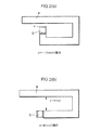
図2はマイクロストリップ導体4の終端部分の様子を説明したものである。マイクロストリップ導体4の終端部分にホールを開けてチップ抵抗5を設けた。いま、マイクロストリップ導体4の窓高yが8mmであるため、空隙長dが1〜7mmの場合は図2(a)に示すようにチップ抵抗5の電極が図2(a)の図面上において上下方向に向いているのに対し、空隙長dが8mmで3辺構造の場合は図2(b)のようにチップ抵抗5の電極は図2(b)の図面上において左右方向を向いている。
【0027】
窓幅10mm、窓高6mmのマイクロストリップ導体4において、空隙長dを変化させた場合、図3に示したようにマイクロストリップ線路40の特性インピーダンスZ0Cは増加し、直線状のストリップ線路40の特性インピーダンスZ0 より大きくなるが、変化は高々10%程度である。空隙長dが8mmの場合、すなわち、図2(b)のように3辺構造となっている場合は特性インピーダンスZ0Cが直線状のストリップ線路40の特性インピーダンスZ0 の値とほぼ等しかった。この場合、マイクロストリップ線路40の面内における上下の線路(マイクロストリップ線路40の終端部とマイクロストリップ線路40と)の結合がきわめて小さいため、特性インピーダンスは直線状のマイクロストリップ線路と等しかったと推察される。
【0028】
空隙長dが8mmの場合と1〜7mmの場合とで特性インピーダンスの傾向が異なる理由としては、図2(a)、(b)に示すように、マイクロストリップ線路40の終端部のホールを開ける方向が図2(a)の場合と図2(b)の場合とで異なっていることが影響していると考えられる。
【0029】
図4は窓幅xとマイクロストリップ線路40の特性インピーダンスとの関係を示したものである。図4は窓高yが6mm、空隙長dが0.5mmの場合の例である。窓幅xの増加とともに特性インピーダンスは増加している。図3の場合と同様に、直線状線路の場合に対して特性インピーダンスの変化は高々10%程度である。
【0030】
図5(a)、(b)はマイクロストリップ導体4を50Ωで終端した場合の入力インピーダンスを測定し、その抵抗分およびリアクタンス分を示したものである。図5はマイクロストリップ導体4の窓幅xが8mm、窓高yが8mm、空隙長dが1mmの場合の例である。比較のためマイクロストリップ導体4によるコイルと寸法が等しい2端子コイルについても測定して比較できるように表示した。図5(a)から2端子コイルの抵抗は共振の影響で12Ω〜210Ωの範囲で大きく変化するのに対し、マイクロストリップ線路40の抵抗は1MHz〜3GHzの周波数において42〜59Ωの小さな変化にとどまっている。これに加え、図5(b)から線路のリアクタンスは2端子コイルの場合よりも小さく、LC共振によって急増することもない。これよりマイクロストリップ線路40のインピーダンスは抵抗分によってほぼ決定され、共振の影響が少なく、高周波特性が優れていることがわかる。
【0031】
次に、磁界センサ1による磁界検出について説明する。
【0032】
図6に示すように、磁界発生のための厚さ2mm、長さ70mmの板状導体を20mm×40mmの断面矩形状に巻き回し、かつ巻き回された板状導体の対向する端部間は電気的に絶縁するべく間隙部11が設けてある断面矩形状の中空矩形筒を形成して励磁コイル10とし、励磁コイル10を形成する中空矩形筒内に磁界センサ1を突出して設け、通電することにより励磁コイル10によって発生する磁界の方向とマイクロストリップ線路40によるコイル面とが直交するように磁界センサ1を取り付け、ネットワークアナライザ12(前記HP8752A)から同軸ケーブル13を介して励磁コイル10を励磁し、マイクロストリップ線路40のコイル面と垂直な外部磁界を印加し、マイクロストリップ線路40からの誘起電圧を同軸ケーブル14を介してネットワークアナライザ12に導いて測定した。
【0033】
この磁界検出の場合における電気的等価回路は図7に示すごとくである。磁界検出において、検出コイルとしてのマイクロストリップ線路40を除去したバックグランド電圧も測定し、マイクロストリップ線路40の誘起電圧からバックグランド電圧を差し引いて誘起電圧とした。
【0034】
この場合、励磁コイル10の共振周波数は700MHzであり、接地導体2の面を含めて、励磁コイル10によって生じた磁界の均一性は±8.9%以内であった。
【0035】
ネットワークアナライザ12から励磁コイル10へ印加した電圧とマイクロストリップ線路40において誘起された電圧とのS21を測定した。S21のゲインより誘起電圧の振幅を求め、S21の位相から磁界に対する誘起電圧の位相差を求めた。100MHz以下であれば同軸ケーブル13、14中の位相変化が無視できるため、S21の位相が磁界と誘起電圧との位相差と考えることができる。
【0036】
図8はマイクロストリップ導体4の窓幅xを変化させた場合の励磁コイル10への印加電圧と誘起電圧との関係を表している。図8は窓幅xが8mm、空隙長dが1mm、印加電圧の周波数が100MHzの場合を例示している。図8から印加電圧と誘起電圧はほぼ比例していることから、この場合も磁界検出が可能であることが明らかである。また、マイクロストリップ導体4の窓幅xと誘起電圧とはほぼ比例している。窓高yは一定であるから、コイルの断面積と誘起電圧は比例していることになる。このような意味ではマイクロストリップ線路40は2端子磁界検出コイルと共通の性質を有していることがわかる。
【0037】
さらに、入力電圧に対する誘起電圧の位相変化は十分小さかった。以上の結果より、マイクロストリップ線路40は磁界検出特性に関しては通常の2端子コイルと同様の特性を有していることがわかった。
【0038】
一方、図9はマイクロストリップ線路40と2端子コイルとで誘起電圧を比較したものである。図9はマイクロストリップ線路40の窓幅xが8mm、窓高yが8mm、空隙長dが1mm、印加電圧の周波数が100MHzの場合の例である。図9は窓幅xが導体線路の形状、寸法は同一であり、2端子コイルはマイクロストリップ線路40から接地導体面を除去した構造である。マイクロストリップ線路40の誘起電圧は2端子コイルの場合の約10%に減少する。すなわちマイクロストリップ線路40は入力インピーダンスが共振の影響をほとんど受けずにGHz帯域の周波数まで安定である一方で、2端子コイルに比較して交番磁界による誘起電圧が小さい点が特徴である。
【0039】
次に、マイクロストリップ線路40の磁界検出のときの誘起電圧、直線状マイクロストリップ線路との比較、接地導体面の影響について説明する。
【0040】
この場合、マイクロストリップ線路40の基本寸法として、窓幅xを10mm、窓高yを6.0mm、空隙長dを0.5mm、接地導体2の高さygを12mmとし、それぞれ表2に示す範囲で変化させた。前記表1に示した例の場合と同様に、(1)式〜(4)式および(5)式に基づき、マイクロストリップ導体4の線路幅wcはマイクロストリップ線路40の特性インピーダンスが50Ωとなるように0.8mmとした。
【0041】
【表2】
磁界センサ1、すなわち、マイクロストリップ線路40の誘起電圧について説明する。
【0043】
図10はマイクロストリップ線路40の誘起電圧と周波数との関係を示したもので、同一寸法の2端子コイルと比較している。図10はマイクロストリップ線路40の窓幅xが10mm、窓高yが6mm、空隙長dが0.5mm、誘電体基板3(εr=5.0、基板厚さtd=0.5mmのテフロン)の高さygが12mm、印加電圧0.5Vの場合の例である。図10(a)はその振幅、図10(b)は位相差を表している。図10(a)から誘起電圧の振幅は周波数に比例して増加し、かつマイクロストリップ線路40の場合、誘起電圧の振幅は2端子コイルよりおよそ1桁小さいことがわかる。また、図10(b)から誘起電圧の位相は印加磁界よりおよそ90°進んでいることがわかる。ただし、マイクロストリップ線路40において1MHz〜10MHzにおいて位相差が90°より小さくなっている点については、接地導体面が影響していると考えられる。
【0044】
次に、マイクロストリップ導体4の寸法を変えて誘起電圧との関係から電圧発生機構について説明する。変数はマイクロストリップ導体4の窓幅x、窓高y、空隙長dとした。図6の測定系において接地導体面の高さygを12mmに固定し、マイクロストリップ線路40の寸法を変化させて磁界検出を行った。図11(a)はマイクロストリップ導体4の窓高yを一定として、窓幅xと誘起電圧の振幅との関係を示したものであり、両者は比例する。また、図11(b)は窓幅xを一定として、窓高yと誘起電圧の振幅との関係を示したものであり、両者はほぼ比例する。ただし、隣接した導体の間隔が小さくなって結合線路の影響が強まる場合は比例傾向からややずれており、磁界検出の機構が複雑化していると考えられる。
【0045】
また、マイクロストリップ線路40の場合、マイクロストリップ線路40の終端部分と近接する線路との間には必ず空隙が存在するため、この影響について説明する。図11(c)に空隙長dと誘起電圧の振幅との関係を示す。空隙長dに関してマイクロストリップ導体4の4辺のうち1辺を除去するところまでdを増加させても、誘起電圧は変化しない。
【0046】
以上のマイクロストリップ線路40の寸法を変えた場合における測定結果から誘起電圧の振幅はマイクロストリップ導体4で囲まれる面積にほぼ比例していることがわかる。これから誘起電圧の振幅が2端子コイルに比較して約1桁小さくなる点を除けば、誘起電圧はファラデーの電磁誘導則によって説明できる。さらに、図11(c)に示した結果は誘起電圧発生時の電流経路が1ターンのマイクロストリップ導体4が切れた終端部分では接地導体面内を通っていることを示している。
【0047】
次に、マイクロストリップ線路40の形状と誘起電圧との関係を明らかにするとともに、1ターンループ以外の形状における誘起電圧の有無について説明する。
【0048】
図12は直線状マイクロストリップ線路20の概観図であり、誘電体基板22の表面上に直線状マイクロストリップ線路20を形成し、直線状マイクロストリップ線路20の一端をチップ抵抗21に接続し、チップ抵抗21の他端を誘電体基板22の裏面に形成した接地導体23に接続して、直線状マイクロストリップ線路20をチップ抵抗21により終端する。この場合、直線状マイクロストリップ線路20の特性インピーダンスは50Ωであり、チップ抵抗21は50Ωの抵抗である。磁界は図12に示すように直線状マイクロストリップ線路20の面に直角な方向に印加した。
【0049】
図13(a)に励磁周波数と誘起電圧の振幅との関係を、図13(b)に励磁周波数と磁界に対する誘起電圧の位相差との関係を示す。
【0050】
マイクロストリップ線路40の場合と比較すると、誘起電圧の振幅が周波数に対して比例していないこと、および磁界と誘起電圧との位相差が0〜30°であり、マイクロストリップ線路40の場合の90°と異なっていること等から磁界検出原理が異なっていることが明らかである。
【0051】
次に、マイクロストリップ線路40の広帯域性について説明する。
【0052】
マイクロストリップ線路40を広帯域で使用するには、特性インピーダンスを50Ω付近に保持することが望ましい。ここではマイクロストリップ線路40の寸法を変えた時の特性インピーダンスの変化を説明する。図14は窓高yの異なるマイクロストリップ線路40の特性インピーダンスZ0Cを測定により求め、直線状マイクロストリップ線路20の特性インピーダンスZC で基準化して示したものである。図14はマイクロストリップ線路40の窓幅xが10mm、空隙長dが0.5mm、接地導体2の高さygを12mmとした場合の例である。隣接する導体の間隔が3mm未満となると線路の結合が起こり、特性インピーダンスが減少する。特性インピーダンスは無損失線路を仮定すると線路の一次定数としてのインダクタンスLa、静電容量Caによって、Z0 =√(La/Ca)となる。ここで逆方向の電流が流れている平行な線路が接近すると負の相互インダクタンスが増加するためにLaが減少し、Caが増加するため、図14の結果は定性的に妥当である。上記の特性インピーダンスのずれは結合線路の影響を考慮した上で特性インピーダンスが50Ωとなる線路幅とすることで解決できる。
【0053】
また、図示していないが、平行なストリップ導体の間隔が3mm以上の場合、および空隙長dを0.3mmからコイルの4辺のうち1辺を切り取った3辺構造とするまで変化させたいずれの場合についても特性インピーダンスはほぼ一定であった。
【0054】
図15はマイクロストリップ線路40と通常の2端子コイルとの入力インピーダンスを比較したものである。マイクロストリップ導体4の窓幅xと窓高yとはそれぞれ10.0mmと6.0mmであって、2端子コイルの寸法は10.0mm×6.0mmで、2端子コイルには50Ωの抵抗を直列に接続した。図15(a)は抵抗分を示し、2端子コイルが共振の影響で20Ω〜180Ωの範囲で大きく変動しているのに対して、マイクロストリップ線路40の場合は40Ω〜60Ωに保たれている。また、図15(b)はリアクタンス分を示し、マイクロストリップ線路40のリアクタンス分は抵抗分に比べて1/10以下であるため入力インピーダンスはほぼ純抵抗とみなせる。
【0055】
入力インピーダンスがほぼ50Ωの純抵抗であることによって広帯域性が得られることは伝送線路の回路理論ではよく知られており、次の通り説明されている。磁界検出の測定系の回路図を示した図7において、Vcは交番磁界によって発生する電圧、Vrはネットワークアナライザ12の内部で観測される50Ω抵抗の端子電圧である。マイクロストリップ線路40の場合、マイクロストリップ線路40を見た入力インピーダンスZinが伝送性の特性インピーダンスZ0 に整合されているため、高周波にわたって観測される電圧VrはVr≒Vc/2となる。これが広帯域に誘起電圧を測定する上での利点である。
【0056】
次に、接地導体面の影響について説明する。
【0057】
マイクロストリップ導体4の寸法を、窓幅xを10.0mm、窓高yを3.0mm、空隙長dを0.5mmに固定し、接地導体面の寸法を変化させたときにおける誘起電圧および入力インピーダンスについて説明する。図16は接地導体面の寸法の説明図である。図16(a)はマイクロストリップ線路40側の表面であり、図16(b)は接地導体面側である。ygは接地導体面の高さであり、hはマイクロストリップ導体4のパターンの内側に設けた開口部30の高さである。開口部30の横幅は10.0mmとマイクロストリップ導体4の窓幅xと等しくした。これはパーミアンス測定装置用の検出コイルにおける開口部30の影響を調べるためである。さらに、図16(b)のwgは開口部30がある場合における接地導体面の幅を表している。測定では接地導体面の寸法を次の3段階にわたって順次小さくした。
(イ) 接地導体面の高さygを12.0mmから5.0mmまで小さくした。
(ロ) マイクロストリップ導体4の内側に幅が10.0mm、高さがhの開口部30を作り、開口部30の高さhを0mmから3.0mmまで大きくした。
(ハ) マイクロストリップ導体4の幅wc0.8mmに対して接地導体面の幅wgを1mmから0.3mmまで小さくした。この手順により変化させた寸法の範囲を表3に示した。
【0058】
【表3】
(イ) 接地導体面の高さygの影響について説明する。
【0060】
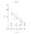
図17は地導体面の高さygとマイクロストリップ線路40の誘起電圧の振幅との関係を示したもので、電圧の値はマイクロストリップ導体4と同一寸法の2端子コイルによる誘起電圧の値V0 で基準化して示した。図17は励磁コイル10に印加した電圧の周波数が10MHz、5MHz、1MHzの場合の例である。図17から接地導体面の高さygが減少するとマイクロストリップ線路40の誘起電圧はほぼ反比例して増大する。これは接地導体面の高さygを減少させると接地導体面の内部を環流する渦電流が減少することを示唆している。
【0061】
この考察に基づきマイクロストリップ導体4によるコイルパターンに鎖交する磁束量をT−Ω法による3次元の電磁界解析から求め、誘起電圧VC をVC =(dφ/dt)/2により計算した結果を図17に示した。dφ/dtを2で除したのは、終端のチップ抵抗5(50Ω)とネットワークアナライザ12の入力抵抗とで分圧するためである。図17によって示した接地導体面の高さygとマイクロストリップ線路40の誘起電圧の振幅の関係は測定結果とよく一致し、解析結果より接地導体面で渦電流が発生し、かつ導体部分の端部に局在化されていることが判った。これより交番磁界の印加により渦電流が生じて、マイクロストリップ導体4を鎖交する磁界強度が減少することが定量的に明らかになった。一方、図17に対応する入力インピーダンスは、図18に示すように、抵抗分が支配的であり接地導体面の高さygによる変化は40Ω〜60Ωの範囲にとどまりインピーダンス整合上問題は少ないことが判る。
(ロ) 開口部の高さhの影響について説明する。
【0062】
図19は接地導体面の開口部30の高さhとマイクロストリップ線路40の誘起電圧の振幅とを示したもので、開口部30の高さhを変えてもマイクロストリップ線路40の誘起電圧の振幅は変化しない。これは渦電流が接地導体面内の端部に集中しているためである。
【0063】
図20は開口部30の高さhを変化させたときの磁界センサ1、すなわち、マイクロストリップ線路40の入力インピーダンスの周波数依存性を示したもので、開口部30の高さhを大きくするにしたがって入力インピーダンスの変化は大きくなる。開口部30の高さhが3mmの場合、すなわち図16(b)のように接地導体面の幅wgがマイクロストリップ導体4の幅wcとほぼ等しい1mmの場合、入力抵抗は35Ω〜70Ωの範囲で大きく変化する。
(ハ) 接地導体面の幅wgの影響について説明する。
【0064】
図21は接地導体面の幅wgとマイクロストリップ線路40の誘起電圧の振幅との関係を示したものであり、接地導体面の幅wgを小さくするとマイクロストリップ線路40の誘起電圧は増加する。接地導体面の幅wgが0mmの値は2端子コイルの場合のマイクロストリップ線路40の誘起電圧を示している。
【0065】
図22は磁界センサ1の入力インピーダンスの周波数依存性を示したものであり、接地導体面の幅wgが1mm、0.8mm、0.6mm、0.3mmの場合と2端子コイルの場合の例である。接地導体面の幅wgが小さくなると磁界センサ1の入力インピーダンスの変化が大きくなる。接地導体面の幅wgを0.3mmまで小さくすると、磁界センサ1の誘起電圧は2端子コイルの約50%まで増加する一方で、入力インピーダンスの変化は30Ω〜100Ωの範囲で大きく変化する。
【0066】
以上、(イ)〜(ハ)から接地導体面を渦電流が環流することによって、マイクロストリップ導体4によるループを鎖交する磁界強度が2端子コイルの場合より減少し、誘起電圧が減少する。渦電流が接地導体面の端部に集中するため、誘起電圧は接地導体面に開口部を設けても変化しない。入力インピーダンスの変化は接地導体面の幅による影響が大きい。入力インピーダンスが50Ωに対して±20%の範囲までの変化を許容するならば、誘起電圧の振幅が2端子コイルの場合の約37%まで増加させることができる。このときの接地導体面の寸法は接地導体面の高さygがマイクロストリップ導体4のループ外形と同程度の大きさである。
【0067】
次に、薄膜によるマイクロストリップ線路の場合について説明する。
【0068】
150μm厚のカバーガラス基板上に銅を膜厚1μmスパッタし、イオントリミングにより1ターン形状に加工してマイクロストリップ線路40とした。マイクロストリップ導体4の幅はマイクロストリップ線路40の特性インピーダンスが50Ωとなるように(1)式〜(4)式より求め、0.31mmとした。
【0069】
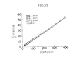
図23は、図2(a)に示した4辺構造であり、マイクロストリップ導体4の窓幅x、窓高yがともに3mmのマイクロストリップ線路40の磁界検出特性を表している。励磁周波数はテフロン基板の場合と同様に100MHzとした。励磁コイル10への印加電圧とマイクロストリップ線路40の誘起電圧はほぼ比例しており、薄膜で作成したマイクロストリップ線路40についても磁界検出が可能であることが判る。また、単位面積当たりの誘起電圧は4辺構造のテフロン基板を用いた場合と比較すると、約30%に低下していた。
【0070】
しかし、上記の結果(図17参照)をもとに、接地導体面の高さygと誘起電圧の振幅が反比例することを仮定すると、接地導体面の寸法を縮小することで、広帯域性を損なわずに誘起電圧を少なくとも4倍以上に大きくできると考えられる。
【0071】
【発明の効果】
以上説明したように本発明の磁界センサによれば、裏面に接地導体が形成された誘電体基板の表面にほぼ1ターンのマクロストリップ導体を形成し、マイクロストリップ線路の特性インピーダンスの抵抗値とほぼ等しい抵抗値を有する抵抗によってマイクロストリップ導体の先端部と接地導体とを電気的に接続してマイクロストリップ導体の先端部を終端して構成したため、マイクロストリップ導体によって囲まれる面に鎖交する磁界によってマイクロストリップ線路に誘起電圧を発生し、この誘起電圧によって磁界の検出ができる効果がある。
【0072】
さらに本発明によれば、マイクロストリップ導体が囲む面積にほぼ比例した誘起電圧を得ることができて磁界を検出することができる効果が得られる。
【0073】
また、本発明の磁界センサによれば、マイクロストリップ導体を薄膜またはプリント基板で形成した場合も同様に磁界の検出ができる効果がある。
【0074】
また、本発明の磁界センサによれば、マイクロストリップ線路の終端部と対向するマイクロストリップ線路との間の空隙長を変化させてもほぼ一定の誘起電圧が得られる効果がある。
【0075】
本発明によれば、接地導体面はマイクロストリップ線路の特性インピーダンスを一定値(50Ω)に保つ役割を果たしており、このためにGHz帯までの高周波の磁界センサとして使用できる。
【0076】
また、本発明の磁界センサによれば、接地導体面の幅、高さを小さくするとマイクロストリップ線路によるコイルパターンの磁界強度が増大するため、大振幅の誘起電圧が得られる効果がある。
【0077】
本発明によれば、接地導体面は特性インピーダンスを上述のように指定値(実施例では(50Ω)に保つ効果(望ましい効果)と同面内の渦電流によりマイクロストリップ線路に誘起される電圧を減少させる効果(望ましくない効果)の双方の役割を有する。したがって、特性インピーダンスを指定値に保ちつつ、接地導体面の寸法を最適化する(幅と高さを小さくする)ことを最適設計の指針とする。
【0078】
また、本発明の磁界センサによれば、特性インピーダンスを設計値に保持したままでマイクロストリップ導体と接地導体面との距離を大きくすれば、大振幅の誘起電圧を得ることができる効果もある。
【図面の簡単な説明】
【図1】本発明にかかる磁界センサの一実施例の構成を示す斜視図である。
【図2】本発明にかかる磁界センサの一実施例におけるマイクロストリップ線路の終端部とチップ抵抗との位置関係を示す平面図である。
【図3】本発明にかかる磁界センサの一実施例における空隙長とZ0C/Z0 との関係を示す特性図である。
【図4】本発明にかかる磁界センサの一実施例における窓幅とZ0C/Z0 との関係を示す特性図である。
【図5】本発明にかかる磁界センサの一実施例における入力インピーダンスの周波数特性図である。
【図6】本発明にかかる磁界センサの一実施例による磁界検出の測定系の概観図である。
【図7】本発明にかかる磁界センサの一実施例による磁界検出の測定系の等価回路図である。
【図8】本発明にかかる磁界センサの一実施例における窓幅をパラメータとしたときの印加電圧対誘起電圧の特性図である。
【図9】本発明にかかる磁界センサの一実施例におけるマイクロストリップ線路と2端子コイルとの磁界検出特性を示す印加電圧対誘起電圧の特性図である。
【図10】本発明にかかる磁界センサの一実施例におけるマイクロストリップ線路と2端子コイルにおける誘起電圧の比較図である。
【図11】本発明にかかる磁界センサの一実施例におけるマイクロストリップ線路のサイズと誘起電圧の振幅との関係を示す特性図である。
【図12】直線状マイクロストリップ線路の斜視図である。
【図13】直線状マイクロストリップ線路の周波数対誘起電圧特性図である。
【図14】本発明にかかる磁界センサの一実施例におけるマイクロストリップ線路の窓高と特性インピーダンスとの関係を示す特性図である。
【図15】本発明にかかる磁界センサの一実施例におけるマイクロストリップ線路の入力インピーダンスの周波数特性図である。
【図16】本発明にかかる磁界センサの一実施例における接地導体面の形状の説明に供する平面図である。
【図17】本発明にかかる磁界センサの一実施例における接地導体面の高さと誘起電圧の振幅との関係を示す特性図である。
【図18】本発明にかかる磁界センサの一実施例における接地導体面の高さと入力インピーダンスとの関係を示す特性図である。
【図19】本発明にかかる磁界センサの一実施例における開口部の高さと誘起電圧の振幅との関係を示す特性図である。
【図20】本発明にかかる磁界センサの一実施例における開口部の高さと入力インピーダンスとの関係を示す特性図である。
【図21】本発明にかかる磁界センサの一実施例における接地導体面の幅と誘起電圧の振幅との関係を示す特性図である。
【図22】本発明にかかる磁界センサの一実施例における接地導体面と入力インピーダンスとの関係を示す特性図である。
【図23】本発明にかかる磁界センサの一実施例における薄膜マイクロストリップ線路の誘起電圧の振幅と印加電圧との関係を示す特性図である。
【符号の説明】
1……磁界センサ
2……接地導体
3……誘電体基板
4……マイクロストリップ導体
5……チップ抵抗
10…励磁コイル
40……マイクロストリップ線路[0001]
[Industrial applications]
The present invention relates to a magnetic field sensor that can be used as a detection coil of a permeance measuring device, and more particularly to a magnetic field sensor using a microstrip line.
[0002]
[Prior art]
As a conventional magnetic field sensor, a magnetoresistive element and a Hall element are generally known.
[0003]
[Problems to be solved by the invention]
However, the above-mentioned conventional magnetic field sensor has a low operating frequency band. For example, in the case of a Hall element, the detection of a high-frequency magnetic field of about 100 kHz is a limit, and the high-frequency magnetic field of a GHz band cannot be detected. There was no detectable magnetic field sensor.
[0004]
An object of the present invention is to provide a magnetic field sensor that can detect a high-frequency magnetic field in a GHz band.
[0005]
In order to achieve the above object, a magnetic field sensor according to the present invention comprises a dielectric substrate having a ground conductor formed on the back surface, a microstrip conductor having approximately one turn formed on the surface of the dielectric substrate, and a microstrip line. Having a resistance value substantially equal to the resistance value of the characteristic impedance of Strike It is characterized by comprising a resistor for electrically connecting the tip of the lip conductor and the ground conductor.
[0006]
[Action]
ADVANTAGE OF THE INVENTION The magnetic field sensor of this invention can detect a high frequency magnetic field based on the induced voltage of the microstrip line induced by linking a magnetic field to the coil formed by the microstrip line.
[0007]
【Example】
Hereinafter, the present invention will be described with reference to examples.
[0008]
FIG. 1 is a perspective view of one embodiment of a magnetic field sensor according to the present invention.
[0009]
In the
[0010]
The
[0011]
Generally, the characteristic impedance Z of a microstrip line 0 Is given by Wheeler as equations (1) to (4).
[0012]
(Equation 1)
(Equation 2)
[Equation 3]
(Equation 4)
In the equations (1) to (4), εr is the relative permittivity of the
[0017]
The width of the
[0018]
Furthermore, the
[0019]
[Table 1]
A printed circuit board and a glass substrate of Teflon are used as the
[0021]
In measuring the basic characteristics of the
[0022]
Characteristic impedance Z of
[0023]
Z 0 = √ (Zshort × Zopen) …… (5)
In the measurement of the characteristic impedance of the
[0024]
Prior to the description of magnetic field detection by the
[0025]
Generally, it is said that the existence range of the electromagnetic field in the
[0026]
FIG. 2 illustrates the state of the terminal portion of the
[0027]
When the gap length d is changed in the
[0028]
The reason why the tendency of the characteristic impedance is different between the case where the gap length d is 8 mm and the case where the gap length d is 1 to 7 mm is to form a hole at the end of the
[0029]
FIG. 4 shows the relationship between the window width x and the characteristic impedance of the
[0030]
FIGS. 5A and 5B show the measured input impedance when the
[0031]
Next, detection of a magnetic field by the
[0032]
As shown in FIG. 6, a plate-like conductor having a thickness of 2 mm and a length of 70 mm for generating a magnetic field is wound in a rectangular shape having a cross section of 20 mm × 40 mm, and a distance between opposed ends of the wound plate-like conductor is A hollow rectangular tube having a rectangular cross section provided with a gap portion 11 for electrical insulation is formed as an
[0033]
The electrical equivalent circuit in the case of this magnetic field detection is as shown in FIG. In the magnetic field detection, the background voltage from which the
[0034]
In this case, the resonance frequency of the
[0035]
S21 of the voltage applied to the
[0036]
FIG. 8 shows the relationship between the voltage applied to the
[0037]
Further, the phase change of the induced voltage with respect to the input voltage was sufficiently small. From the above results, it was found that the
[0038]
On the other hand, FIG. 9 compares the induced voltage between the
[0039]
Next, the induced voltage at the time of detecting the magnetic field of the
[0040]
In this case, as the basic dimensions of the
[0041]
[Table 2]
The induced voltage of the
[0043]
FIG. 10 shows the relationship between the induced voltage of the
[0044]
Next, the voltage generation mechanism will be described based on the relationship with the induced voltage by changing the dimensions of the
[0045]
Further, in the case of the
[0046]
From the measurement results when the dimensions of the
[0047]
Next, the relationship between the shape of the
[0048]
FIG. 12 is a schematic view of the
[0049]
FIG. 13A shows the relationship between the excitation frequency and the amplitude of the induced voltage, and FIG. 13B shows the relationship between the excitation frequency and the phase difference of the induced voltage with respect to the magnetic field.
[0050]
Compared with the case of the
[0051]
Next, the broadband property of the
[0052]
In order to use the
[0053]
Also, although not shown, in the case where the interval between the parallel strip conductors is 3 mm or more, and the gap length d is changed from 0.3 mm to a three-sided structure obtained by cutting one of four sides of the coil. Also in the case of the above, the characteristic impedance was almost constant.
[0054]
FIG. 15 compares the input impedances of the
[0055]
It is well known in the circuit theory of a transmission line that an input impedance is a pure resistance of about 50Ω to obtain a wide band, and is described as follows. In FIG. 7 showing a circuit diagram of a measurement system for magnetic field detection, Vc is a voltage generated by an alternating magnetic field, and Vr is a terminal voltage of a 50Ω resistor observed inside the
[0056]
Next, the influence of the ground conductor surface will be described.
[0057]
The dimensions of the
(A) The height yg of the ground conductor surface was reduced from 12.0 mm to 5.0 mm.
(B) An
(C) The width wg of the ground conductor surface is reduced from 1 mm to 0.3 mm with respect to the width wc of the
[0058]
[Table 3]
(B) The effect of the height yg of the ground conductor surface will be described.
[0060]
FIG. 17 shows the relationship between the height yg of the ground conductor surface and the amplitude of the induced voltage of the
[0061]
Based on this consideration, the amount of magnetic flux interlinking the coil pattern formed by the
(B) The effect of the height h of the opening will be described.
[0062]
FIG. 19 shows the height h of the
[0063]
FIG. 20 shows the frequency dependence of the input impedance of the
(C) The influence of the width wg of the ground conductor surface will be described.
[0064]
FIG. 21 shows the relationship between the width wg of the ground conductor surface and the amplitude of the induced voltage of the
[0065]
FIG. 22 shows the frequency dependence of the input impedance of the
[0066]
As described above, the eddy current circulates through the ground conductor surface from (a) to (c), whereby the magnetic field strength interlinking the loop formed by the
[0067]
Next, the case of a microstrip line using a thin film will be described.
[0068]
Copper was sputtered at a thickness of 1 μm on a cover glass substrate having a thickness of 150 μm, and processed into a one-turn shape by ion trimming to form a
[0069]
FIG. 23 shows the four-sided structure shown in FIG. 2A, and shows the magnetic field detection characteristics of the
[0070]
However, assuming that the height yg of the grounding conductor surface and the amplitude of the induced voltage are inversely proportional based on the above result (see FIG. 17), the size of the grounding conductor surface is reduced, thereby impairing the broadband performance. It can be considered that the induced voltage can be increased at least four times or more without any change.
[0071]
【The invention's effect】
As described above, according to the magnetic field sensor of the present invention, the macrostrip conductor of approximately one turn is formed on the surface of the dielectric substrate having the ground conductor formed on the back surface, and the resistance value of the characteristic impedance of the microstrip line is substantially equal to that of the microstrip line. The tip of the microstrip conductor is electrically connected to the ground conductor by a resistor having an equal resistance value to terminate the tip of the microstrip conductor. An induced voltage is generated in the microstrip line, and the magnetic field can be detected by the induced voltage.
[0072]
Further, according to the present invention, it is possible to obtain an induced voltage that is substantially proportional to the area surrounded by the microstrip conductor and to detect a magnetic field.
[0073]
Further, according to the magnetic field sensor of the present invention, the magnetic field can be similarly detected even when the microstrip conductor is formed of a thin film or a printed circuit board.
[0074]
Further, according to the magnetic field sensor of the present invention, there is an effect that a substantially constant induced voltage can be obtained even when the gap length between the end portion of the microstrip line and the opposing microstrip line is changed.
[0075]
According to the present invention, the ground conductor surface plays a role of maintaining the characteristic impedance of the microstrip line at a constant value (50Ω), and thus can be used as a high-frequency magnetic field sensor up to the GHz band.
[0076]
Further, according to the magnetic field sensor of the present invention, when the width and height of the ground conductor surface are reduced, the magnetic field strength of the coil pattern formed by the microstrip line increases, so that there is an effect that a large amplitude induced voltage can be obtained.
[0077]
According to the present invention, the ground conductor surface has the effect of maintaining the characteristic impedance at the specified value (in the embodiment, (50Ω) in the embodiment (desirable effect)) as described above and the voltage induced in the microstrip line by the eddy current in the same plane. It has the role of both reducing effect (undesired effect), so it is necessary to optimize the dimensions (reduce the width and height) of the ground conductor surface while keeping the characteristic impedance at a specified value. And
[0078]
Further, according to the magnetic field sensor of the present invention, if the distance between the microstrip conductor and the ground conductor surface is increased while maintaining the characteristic impedance at the design value, there is also an effect that a large amplitude induced voltage can be obtained.
[Brief description of the drawings]
FIG. 1 is a perspective view showing a configuration of an embodiment of a magnetic field sensor according to the present invention.
FIG. 2 is a plan view showing a positional relationship between a terminal portion of a microstrip line and a chip resistor in one embodiment of the magnetic field sensor according to the present invention.
FIG. 3 shows the gap length and Z in one embodiment of the magnetic field sensor according to the present invention. 0C / Z 0 FIG. 9 is a characteristic diagram showing a relationship with the graph.
FIG. 4 shows a window width and Z in one embodiment of the magnetic field sensor according to the present invention. 0C / Z 0 FIG. 9 is a characteristic diagram showing a relationship with the graph.
FIG. 5 is a frequency characteristic diagram of an input impedance in one embodiment of the magnetic field sensor according to the present invention.
FIG. 6 is a schematic view of a measurement system for magnetic field detection by one embodiment of the magnetic field sensor according to the present invention.
FIG. 7 is an equivalent circuit diagram of a measurement system for magnetic field detection by one embodiment of the magnetic field sensor according to the present invention.
FIG. 8 is a characteristic diagram of applied voltage versus induced voltage when a window width is used as a parameter in one embodiment of the magnetic field sensor according to the present invention.
FIG. 9 is a characteristic diagram of applied voltage versus induced voltage, showing the magnetic field detection characteristics of the microstrip line and the two-terminal coil in one embodiment of the magnetic field sensor according to the present invention.
FIG. 10 is a comparison diagram of induced voltages in a microstrip line and a two-terminal coil in one embodiment of the magnetic field sensor according to the present invention.
FIG. 11 is a characteristic diagram showing a relationship between the size of a microstrip line and the amplitude of an induced voltage in one embodiment of the magnetic field sensor according to the present invention.
FIG. 12 is a perspective view of a linear microstrip line.
FIG. 13 is a graph showing frequency versus induced voltage characteristics of a linear microstrip line.
FIG. 14 is a characteristic diagram showing a relationship between a window height of a microstrip line and a characteristic impedance in one embodiment of the magnetic field sensor according to the present invention.
FIG. 15 is a frequency characteristic diagram of the input impedance of the microstrip line in one embodiment of the magnetic field sensor according to the present invention.
FIG. 16 is a plan view for describing the shape of a ground conductor surface in one embodiment of the magnetic field sensor according to the present invention.
FIG. 17 is a characteristic diagram showing the relationship between the height of the ground conductor surface and the amplitude of the induced voltage in one embodiment of the magnetic field sensor according to the present invention.
FIG. 18 is a characteristic diagram showing the relationship between the height of the ground conductor surface and the input impedance in one embodiment of the magnetic field sensor according to the present invention.
FIG. 19 is a characteristic diagram showing the relationship between the height of the opening and the amplitude of the induced voltage in one embodiment of the magnetic field sensor according to the present invention.
FIG. 20 is a characteristic diagram showing a relationship between an opening height and an input impedance in one embodiment of the magnetic field sensor according to the present invention.
FIG. 21 is a characteristic diagram showing the relationship between the width of the ground conductor surface and the amplitude of the induced voltage in one embodiment of the magnetic field sensor according to the present invention.
FIG. 22 is a characteristic diagram showing a relationship between a ground conductor surface and an input impedance in one embodiment of the magnetic field sensor according to the present invention.
FIG. 23 is a characteristic diagram showing the relationship between the amplitude of the induced voltage and the applied voltage of the thin-film microstrip line in one embodiment of the magnetic field sensor according to the present invention.
[Explanation of symbols]
1 ... magnetic field sensor
2 Ground conductor
3 ... Dielectric substrate
4. Microstrip conductor
5 Chip resistance
10 Excitation coil
40 ... microstrip line
Claims (3)
Priority Applications (1)
| Application Number | Priority Date | Filing Date | Title |
|---|---|---|---|
| JP29070494A JP3542183B2 (en) | 1994-10-31 | 1994-10-31 | Magnetic field sensor |
Applications Claiming Priority (1)
| Application Number | Priority Date | Filing Date | Title |
|---|---|---|---|
| JP29070494A JP3542183B2 (en) | 1994-10-31 | 1994-10-31 | Magnetic field sensor |
Publications (2)
| Publication Number | Publication Date |
|---|---|
| JPH08129058A JPH08129058A (en) | 1996-05-21 |
| JP3542183B2 true JP3542183B2 (en) | 2004-07-14 |
Family
ID=17759439
Family Applications (1)
| Application Number | Title | Priority Date | Filing Date |
|---|---|---|---|
| JP29070494A Expired - Fee Related JP3542183B2 (en) | 1994-10-31 | 1994-10-31 | Magnetic field sensor |
Country Status (1)
| Country | Link |
|---|---|
| JP (1) | JP3542183B2 (en) |
Families Citing this family (9)
| Publication number | Priority date | Publication date | Assignee | Title |
|---|---|---|---|---|
| JP2970615B2 (en) * | 1997-08-29 | 1999-11-02 | 日本電気株式会社 | Magnetic field detector |
| US6750648B1 (en) | 1997-08-29 | 2004-06-15 | Nec Corporation | Magnetic field detector having a dielectric looped face |
| JPH11166963A (en) | 1997-12-04 | 1999-06-22 | Kyodo Kumiai Joint Labo Sendai | Magnetic field direction detection method |
| JP4318820B2 (en) * | 1999-12-09 | 2009-08-26 | 株式会社日本自動車部品総合研究所 | Magnetic detection antenna |
| JP4219634B2 (en) * | 2002-08-01 | 2009-02-04 | 凌和電子株式会社 | Magnetic sensor, side-open TEM cell, and apparatus using them |
| JP4505338B2 (en) * | 2003-01-31 | 2010-07-21 | コミサリア、ア、レネルジ、アトミク−セーエーアー | Elements for sensing radio frequency magnetic fields |
| JP5024587B2 (en) * | 2005-12-07 | 2012-09-12 | 日本電気株式会社 | Magnetic field detector and current measuring method used for magnetic field and current measurement |
| CN105551675B (en) * | 2012-07-30 | 2017-06-13 | 株式会社村田制作所 | Flat cable |
| JP6853441B2 (en) * | 2019-04-24 | 2021-03-31 | 健二 飯島 | Magnetic sensor element, magnetic detector, motor with magnetic sensor element and device with magnetic detector |
-
1994
- 1994-10-31 JP JP29070494A patent/JP3542183B2/en not_active Expired - Fee Related
Also Published As
| Publication number | Publication date |
|---|---|
| JPH08129058A (en) | 1996-05-21 |
Similar Documents
| Publication | Publication Date | Title |
|---|---|---|
| Hoefer | Equivalent series inductivity of a narrow transverse slit in microstrip | |
| US10014564B2 (en) | Dielectric waveguide resonator and filter comprised of a pair of dielectric blocks having opposing surfaces coupled to each other by a probe | |
| Olthuis et al. | Theoretical and experimental determination of cell constants of planar-interdigitated electrolyte conductivity sensors | |
| JP3542183B2 (en) | Magnetic field sensor | |
| JP2003110307A (en) | Dielectric waveguide filter and mounting structure thereof | |
| Williams | Metal-insulator-semiconductor transmission lines | |
| JP2002135003A (en) | Waveguide-type dielectric filter | |
| JP5418424B2 (en) | Electromagnetic field probe | |
| JP3292531B2 (en) | High frequency excitation plasma measurement device | |
| JPWO2009011168A1 (en) | Microstrip line filter and manufacturing method thereof | |
| CN1124539A (en) | Transmission line and method of designing same | |
| US6320376B1 (en) | Magnetic field sensor and system for measuring a magnetic field including a plurality of conductors electrically connected in a loop | |
| JP7016238B2 (en) | Directional coupler | |
| Roschmann | Compact YIG bandpass filter with finite-pole frequencies for applications in microwave integrated circuits (short papers) | |
| JPH1082845A (en) | Magnetic field sensor | |
| JPH0369203B2 (en) | ||
| JP2021162327A (en) | Permeability measurement probe and permeability measurement device using the same | |
| WO2023228930A1 (en) | Magnetic permeability measurement probe and magnetic permeability measurement device using same | |
| JP2003294793A (en) | Inductor measuring tool for electronic part and its method | |
| JP3794437B2 (en) | Waveguide device, electrical property measuring device, and electrical property measuring method | |
| JP2003207531A (en) | Near magnetic field probe | |
| US20230025196A1 (en) | Permeability Measuring Probe and Permeability Measuring Device | |
| CN217691592U (en) | Adjustable-attenuation balance filter | |
| TW484248B (en) | Micro-strip line having switchable characteristic impedance | |
| JPH07104044A (en) | Magnetic permeability measuring device |
Legal Events
| Date | Code | Title | Description |
|---|---|---|---|
| A131 | Notification of reasons for refusal |
Free format text: JAPANESE INTERMEDIATE CODE: A131 Effective date: 20031216 |
|
| A521 | Written amendment |
Free format text: JAPANESE INTERMEDIATE CODE: A523 Effective date: 20040130 |
|
| TRDD | Decision of grant or rejection written | ||
| A01 | Written decision to grant a patent or to grant a registration (utility model) |
Free format text: JAPANESE INTERMEDIATE CODE: A01 Effective date: 20040309 |
|
| A61 | First payment of annual fees (during grant procedure) |
Free format text: JAPANESE INTERMEDIATE CODE: A61 Effective date: 20040330 |
|
| R150 | Certificate of patent or registration of utility model |
Free format text: JAPANESE INTERMEDIATE CODE: R150 |
|
| R250 | Receipt of annual fees |
Free format text: JAPANESE INTERMEDIATE CODE: R250 |
|
| FPAY | Renewal fee payment (event date is renewal date of database) |
Free format text: PAYMENT UNTIL: 20090409 Year of fee payment: 5 |
|
| FPAY | Renewal fee payment (event date is renewal date of database) |
Free format text: PAYMENT UNTIL: 20100409 Year of fee payment: 6 |
|
| FPAY | Renewal fee payment (event date is renewal date of database) |
Free format text: PAYMENT UNTIL: 20110409 Year of fee payment: 7 |
|
| FPAY | Renewal fee payment (event date is renewal date of database) |
Free format text: PAYMENT UNTIL: 20120409 Year of fee payment: 8 |
|
| FPAY | Renewal fee payment (event date is renewal date of database) |
Free format text: PAYMENT UNTIL: 20120409 Year of fee payment: 8 |
|
| FPAY | Renewal fee payment (event date is renewal date of database) |
Free format text: PAYMENT UNTIL: 20130409 Year of fee payment: 9 |
|
| LAPS | Cancellation because of no payment of annual fees |