JP6848559B2 - Time measuring device and distance measuring device - Google Patents
Time measuring device and distance measuring device Download PDFInfo
- Publication number
- JP6848559B2 JP6848559B2 JP2017049636A JP2017049636A JP6848559B2 JP 6848559 B2 JP6848559 B2 JP 6848559B2 JP 2017049636 A JP2017049636 A JP 2017049636A JP 2017049636 A JP2017049636 A JP 2017049636A JP 6848559 B2 JP6848559 B2 JP 6848559B2
- Authority
- JP
- Japan
- Prior art keywords
- sequence
- reference clock
- progress
- delay
- time
- Prior art date
- Legal status (The legal status is an assumption and is not a legal conclusion. Google has not performed a legal analysis and makes no representation as to the accuracy of the status listed.)
- Active
Links
Images


Landscapes
- Optical Radar Systems And Details Thereof (AREA)
- Measurement Of Optical Distance (AREA)
- Manipulation Of Pulses (AREA)
Description
本発明は、時間計測装置、および距離計測装置に関する。 The present invention relates to a time measuring device and a distance measuring device.
従来、あるタイミングで生成された信号と、当該タイミングよりも遅いタイミングで生成が開始され配線を通過した信号とが入力され、上記あるタイミングで生成された信号と上記遅いタイミングで生成された信号との入力タイミングの時間差を測定する回路がある(例えば、特許文献1、2)。
Conventionally, a signal generated at a certain timing and a signal whose generation is started later than the timing and passed through the wiring are input, and a signal generated at the above-mentioned timing and a signal generated at the above-mentioned later timing are input. There is a circuit for measuring the time difference of the input timing of (for example,
上記特許文献1、2に開示された回路については、時間差の測定精度が温度変化の影響を受ける、という観点において改善の余地があった。
本発明は、時間差の測定精度について、温度変化の影響を受けづらい時間計測装置を提供することを目的とする。
The circuits disclosed in
An object of the present invention is to provide a time measuring device that is less susceptible to temperature changes in terms of time difference measurement accuracy.
上記の課題を解決し、目的を達成するために、本発明に係る時間計測装置は、複数の遅延素子を有する遅延回路と、所定の周期で基準クロックを出力する基準クロック生成部と、を有する時間計測装置であって、前記遅延回路には、パルス信号である被測定信号が入力され、該遅延回路は、該被測定信号の速度を遅らせて回路内を通過させ、前記基準クロック生成部は、測定開始信号に基づいて、前記基準クロックを開始し、前記時間計測装置は、前記基準クロックの1周期毎に、前記遅延回路における各遅延素子の電位を読み出し、該読み出した電位が閾値に基づき、高いレベルを0または1の一方とし、低いレベルを0または1の他方とすることで、前記複数の遅延素子の個数に応じた進行状況数列を作成し、前記基準クロックの周期と、前記遅延素子の遅延時間と、前記進行状況数列における01または10の変化位置に対応する遅延素子の個数、とに基づいて、前記測定開始信号から前記被測定信号におけるパルスの立ち上がり、または立下りまでの時間を計測する時間測定部と、を有し、前記基準クロックを前記遅延回路へ入力して、該基準クロックの進行状況数列を作成することで、該基準クロックの1周期に対応する前記遅延回路における遅延素子の個数を求めるキャリブレーション制御により前記遅延素子の遅延時間を求め、前記時間測定部は、前記測定開始信号から前記被測定信号におけるパルスの立ち上がり、または立下りまでの時間を計測する際に、前記求めた遅延素子の遅延時間を用いることを特徴とする。 In order to solve the above problems and achieve the object, the time measuring device according to the present invention includes a delay circuit having a plurality of delay elements and a reference clock generator that outputs a reference clock at a predetermined cycle. In the time measuring device, a signal to be measured, which is a pulse signal, is input to the delay circuit, the delay circuit delays the speed of the signal to be measured and passes through the circuit, and the reference clock generator , The reference clock is started based on the measurement start signal, and the time measuring device reads out the potential of each delay element in the delay circuit for each cycle of the reference clock, and the read potential is based on the threshold value. By setting the high level to one of 0 or 1 and the low level to the other of 0 or 1, a progress number sequence corresponding to the number of the plurality of delay elements is created, and the period of the reference clock and the delay are described. The time from the measurement start signal to the rise or fall of the pulse in the measured signal based on the delay time of the elements and the number of delay elements corresponding to the change positions of 01 or 10 in the progress number sequence. In the delay circuit corresponding to one cycle of the reference clock, the reference clock is input to the delay circuit to create a progress number sequence of the reference clock. The delay time of the delay element is obtained by calibration control for obtaining the number of delay elements, and the time measuring unit measures the time from the measurement start signal to the rise or fall of the pulse in the signal to be measured. It is characterized in that the delay time of the delay element obtained is used.
本発明によれば、温度の影響を少なくして、精度よく時間差を測定することができる。 According to the present invention, the influence of temperature can be reduced and the time difference can be measured with high accuracy.
図1は、時間計測装置100のブロック図である。時間計測装置100は、測定開始信号の入力タイミングと被測定信号(パルス信号)の立ち上がりエッジまたは立ち下がりエッジまでの時間を計測する装置である。時間計測回路本体102は、被測定信号(パルス信号)の速度を遅らせて回路を進行させる遅延素子を有する回路である。図1および図2に示すように、時間計測回路本体102は、直列に繋がれた遅延素子列1021と、フリップフロップ列1022とを有している。
FIG. 1 is a block diagram of the
時間計測回路本体102は、基準クロック発生部105により出力された基準クロックの周期毎に、遅延素子列1021における被測定信号(パルス信号)の進行状況を表す進行状況数列(詳細は後述する)を生成する。具体的には、被測定信号(パルス信号)がN個の遅延素子(遅延素子1〜遅延素子N)が直列に連結された遅延素子列1021に入力されると、基準クロック生成部105は、基準クロックをフリップフロップ列1022へ入力する。各遅延素子の入力信号レベルは基準クロックに同期してフリップフロップ列1022により、進行状況数列として保持される。測定対象信号が入力されている遅延素子は高電位状態”1”を、それ以外の遅延素子は低電位状態”0”を示す。フリップフロップ列1022に保持される進行状況数列は、時間測定部200内のメモリ202へ保持される。
The time measurement circuit
図9は、時間測定部200のブロック図である。時間測定部200は、フリップフロップ列1022から読み出した進行状況数列を保存するメモリ202と、時間測定部200を制御する時間測定部制御部201を備える。時間測定部制御部201は、キャリブレーション制御部2011、数列解析部2012、および数値化演算部2013を備える。メモリ202は、保存用メモリ2021、および解析用メモリ2022を備える。
FIG. 9 is a block diagram of the time measuring unit 200. The time measurement unit 200 includes a memory 202 that stores a progress sequence read from the flip-flop sequence 1022, and a time measurement unit control unit 201 that controls the time measurement unit 200. The time measurement unit control unit 201 includes a
図2を用いて、時間計測回路本体102が進行状況数列を出力する動作を説明する。
以降の説明では、基準クロックの立ち上がりに応じて、フリップフロップ列1022から進行状況数列を読み出すものとして説明する。ある基準クロックの立ち上がり時に、例えば、図2のように遅延素子列1021上の6番目から8番目の遅延素子の電位が立ち上がっているような電位分布となっている場合、時間計測回路本体102は、その電位を検知したことを示す信号列Nを含む進行状況数列を出力する。つまり、進行状況数列は、遅延素子列1021内の電位分布を示す信号列である。例えば、進行状況数列は、遅延素子列1021上の高電位部分に対応して出力される信号(例えば、1)列と、遅延素子列1021上の低電位部分であることを示す信号(例えば、0)列とにより構成される。
The operation of the time measurement circuit
In the following description, it is assumed that the progress sequence is read from the flip-flop sequence 1022 according to the rising edge of the reference clock. When the potential distribution of the sixth to eighth delay elements on the delay element train 1021 rises at the rise of a certain reference clock, for example, the time measurement circuit
このように、進行状況数列は、基準クロック発生部105から出力される基準クロックの周期毎に、被測定信号(パルス信号)の進行状況を表す数列である。進行状況数列における1ビットは、遅延素子列1021における個々の素子に対応する。進行状況数列は、次の基準クロックの立ち上がり時までフリップフロップ列1022に保持される。この保持期間にこの進行状況数列を時間計測回路本体102から時間測定部200内のメモリ202に転送し、進行状況数列を任意の期間記憶しておく。
As described above, the progress sequence is a sequence representing the progress of the signal to be measured (pulse signal) for each cycle of the reference clock output from the reference clock generation unit 105. One bit in the progress sequence corresponds to an individual element in the delay element sequence 1021. The progress sequence is held in the flip-flop sequence 1022 until the next rise of the reference clock. During this holding period, the progress sequence is transferred from the time measurement circuit
図2では、0から10までの11個の遅延素子を構成した遅延回路を例示したが、遅延素子の個数は、1回の取得で計測する時間の長さに応じて設定される。既述したように、基準クロックの周期毎に進行状況数列を取得するので、遅延素子の数は、遅延素子の遅延時間の合計が基準クロックの1周期の時間以上である必要がある。例えば、基準クロックの周期が5nsec(ナノセック)、遅延素子の遅延時間が80psec(ピコセック)であるとすると、遅延素子の数は、63個(80psec × 63 = 5.04nsec)必要である。ただし、遅延素子の遅延時間は温度により変化し、低温になると高速となる。記述した遅延素子の場合、常温(25℃)では遅延時間が80psecであるが、10℃未満になると60psecとなる。そこで、温度変化による遅延素子の遅延時間の変化分を見込んで、遅延素子の数を設定することが望ましい。説明した例の場合、遅延素子の数は、63個の約倍である120個程度とすることが望ましい。遅延素子列1021における遅延素子の数は、遅延素子の遅延時間が温度変化により変化しても、遅延素子の遅延時間の合計が基準クロックの1周期の時間以上となる数となっている。 In FIG. 2, a delay circuit in which 11 delay elements from 0 to 10 are configured is illustrated, but the number of delay elements is set according to the length of time measured in one acquisition. As described above, since the progress sequence is acquired for each cycle of the reference clock, the total number of delay elements of the delay elements needs to be equal to or longer than the time of one cycle of the reference clock. For example, assuming that the period of the reference clock is 5 nsec (nanosec) and the delay time of the delay element is 80 psec (picosec), the number of delay elements needs to be 63 (80 psec × 63 = 5.04 nsec). However, the delay time of the delay element changes depending on the temperature, and becomes faster at low temperatures. In the case of the described delay element, the delay time is 80 psec at room temperature (25 ° C), but it becomes 60 psec when the temperature is less than 10 ° C. Therefore, it is desirable to set the number of delay elements in consideration of the change in the delay time of the delay elements due to the temperature change. In the case of the described example, it is desirable that the number of delay elements is about 120, which is about twice 63. The number of delay elements in the delay element sequence 1021 is such that the total delay time of the delay elements is equal to or longer than the time of one cycle of the reference clock even if the delay time of the delay elements changes due to a temperature change.
ここで、本明細書における進行状況数列における数列の並びと時間軸との関係について、説明する。図1および図2に示した時間計測回路本体102では、入力端子が紙面左側にあるので、被測定信号(パルス信号)は、紙面左側から紙面右側へと進む。そこで、進行状況数列は、紙面左側端部のビットをLSB(Least-Significant Bit)、紙面右側端部のビットをMSB(Most-significant Bit)とする。換言すると、進行状況数列の紙面左側端部のビット(LSB)が最も新しいビットであり、進行状況数列の紙面右側端部のビットをMSBが最も古いビットである。例えば、図2に示した例において、遅延素子の遅延時間が80psec(ピコセック)であるとすると、遅延素子列1021上の6番目のデータは、進行状況数列として読み出したタイミングから560 psec(80psec × 7 = 560 psec)前の被測定信号(パルス信号)の信号レベルを表している。
Here, the relationship between the sequence of the sequence and the time axis in the sequence of progress in the present specification will be described. In the time measurement circuit
<キャリブレーション制御>
キャリブレーション制御について説明する。既述したように、遅延素子の遅延時間は温度により変化するので、基準クロックの1周期に対応する遅延素子の数を定期的に確認する。この基準クロックの1周期に対応する遅延素子の数を確認する制御を、本明細書では、キャリブレーション制御と呼ぶ。
<Calibration control>
Calibration control will be described. As described above, since the delay time of the delay element changes depending on the temperature, the number of delay elements corresponding to one cycle of the reference clock is periodically checked. In this specification, the control for confirming the number of delay elements corresponding to one cycle of the reference clock is referred to as calibration control.
図10に示すように、キャリブレーション制御は、時間計測回路本体102内の遅延素子列1021へ、基準クロック生成部105で生成された基準クロックを被測定信号として入力することで行なう。すなわち、キャリブレーション制御において、基準クロック生成部105で生成された基準クロックは、進行状況数列を取得するためにフリップフロップ列1022へ入力する基準クロックと被測定信号として遅延素子列1021へ入力する基準クロックという2系統の基準クロックが存在する。
As shown in FIG. 10, the calibration control is performed by inputting the reference clock generated by the reference clock generation unit 105 as a signal to be measured to the delay element string 1021 in the time measurement circuit
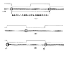
図3に、キャリブレーション制御で得られる進行状況数列の一例を示す。ここで、“10”という並びになっている間の信号列の桁数が基準クロックの周期に対応する遅延素子列の個数となる(A)。ところで、基準クロック生成部105から遅延素子列1021までの配線長とフリップフロップ列1022から遅延素子列1021までの配線長とが異なることに起因して、フリップフロップ列1022へ入力する基準クロックの位相と被測定信号として遅延素子列1021へ入力する基準クロックの位相とは異なる場合がある。 FIG. 3 shows an example of a progress sequence obtained by calibration control. Here, the number of digits of the signal sequence during the sequence of "10" is the number of delay element sequences corresponding to the cycle of the reference clock (A). By the way, the phase of the reference clock input to the flip-flop row 1022 is due to the difference between the wiring length from the reference clock generation unit 105 to the delay element row 1021 and the wiring length from the flip-flop row 1022 to the delay element row 1021. And may be different from the phase of the reference clock input to the delay element string 1021 as the signal to be measured.
フリップフロップ列1022へ入力する基準クロックの位相と被測定信号として遅延素子列1021へ入力する基準クロックの位相とが異なる場合、例えば、(B)に示すような状況が生じ得る。(B)では、進行状況数列のうち、立ち上がり時の電位分布に対応して出力される信号の終端(すなわち、“10”という並び)が検出できないため、基準クロックの周期に対応する遅延素子列の個数が分からない。この(B)の例では、nクロック目の進行状況数列における立ち下がり(または立ち上がり)位置は検出できたものの、同じタイミングで立ち上がり(または立ち上下がり)位置を検出することができず、遅延素子列の個数が分からなくなる。このような場合、(C)のように、被測定信号として遅延素子列1021へ入力する基準クロックを、基準クロック生成部105にて、フリップフロップ列1022へ入力する基準クロックに対して180度位相をずらしたクロックとして延素子列1021へ入力すれば、進行状況数列のうち、立ち上がり時の電位分布に対応して出力される信号の先端E1と終端E2(すなわち、“10”という並び)とを同じタイミングで検出できるため、基準クロックの周期に対応する遅延素子列の個数が分かる。 When the phase of the reference clock input to the flip-flop sequence 1022 and the phase of the reference clock input to the delay element sequence 1021 as the signal to be measured are different, for example, the situation shown in (B) may occur. In (B), since the end of the signal output corresponding to the potential distribution at the rising edge (that is, the sequence of "10") cannot be detected in the progress sequence, the delay element sequence corresponding to the cycle of the reference clock. I don't know the number of. In this example (B), although the falling (or rising) position in the progress sequence of the nth clock can be detected, the rising (or rising / falling) position cannot be detected at the same timing, and the delay element. I don't know the number of columns. In such a case, as shown in (C), the reference clock input to the delay element string 1021 as the signal to be measured is 180-degree phase with respect to the reference clock input to the flip-flop sequence 1022 by the reference clock generation unit 105. If the clock is input to the extension element string 1021 as a shifted clock, the tip E1 and the end E2 (that is, the sequence of "10") of the signal output corresponding to the potential distribution at the rising edge of the progress sequence are displayed. Since it can be detected at the same timing, the number of delay element trains corresponding to the reference clock cycle can be known.
フリップフロップ列1022から取り込んだ進行状況数列は、時間測定部200内のメモリ202に転送され、メモリ202内の保存用メモリ2021へ保存される。そして、既述したキャリブレーション制御は、時間測定部200内にある時間測定部制御部201におけるキャリブレーション制御部2011で実行される。
The progress sequence taken from the flip-flop sequence 1022 is transferred to the memory 202 in the time measuring unit 200 and stored in the
基準クロック発生部105から出力される基準クロックは、時間計測する間隔(時間計測するフレームレート)を早くしたいので、既述したように、5nsecというような高速なクロックで実行される。このような高速なクロックで、時間測定部制御部201を駆動しようとすると、高速クロックに対応できる演算回路は高価であり、また演算量が多いと発熱量も多くなる。そこで、時間測定部制御部201は、基準クロック発生部105から出力される基準クロックよりも低速の解析用クロックにより駆動される。 Since the reference clock output from the reference clock generation unit 105 wants to increase the time measurement interval (time measurement frame rate), it is executed with a high-speed clock such as 5 nsec as described above. If the time measurement unit control unit 201 is to be driven by such a high-speed clock, the arithmetic circuit capable of supporting the high-speed clock is expensive, and if the arithmetic amount is large, the heat generation amount is also large. Therefore, the time measurement unit control unit 201 is driven by an analysis clock that is slower than the reference clock output from the reference clock generation unit 105.
キャリブレーション制御部2011は、基準クロックの周期を既述したキャリブレーション制御により求めた基準クロックの周期に対応する遅延素子列の個数で割ることによって遅延素子1個当たりの遅延時間を算出する。算出した遅延素子1個当たりの遅延時間は、メモリ202に保存される。
The
また、キャリブレーション制御部2011は、基準クロックの周期に対応する遅延素子列の個数だけ、LSBから”1”である信号列と、それ以降は”0”である信号列とから構成されるマスク数列を生成する(図4)。このマスク数列の効果については後述する。このマスタ数列の全ビット数は、遅延素子列1021における遅延素子の全個数に対応する。
Further, the
<時間計測>
時間計測について説明する。既述したように、時間計測装置100は、基準クロック発生部105により出力された基準クロックの周期毎に、時間計測回路本体102内の遅延素子列1021における被測定信号(パルス信号)の進行状況を表す進行状況数列を取り込む。この取り込んだ進行状況数列は、記述したキャリブレーション制御の場合と同様に、時間測定部200内のメモリ202に転送され、メモリ202内の保存用メモリ2021へ保存される。
<Time measurement>
Time measurement will be described. As described above, the
数列解析部2012取り込んだ進行状況数列から、測定開始信号の入力タイミングと被測定信号(パルス信号)の立ち上がりエッジまたは立ち下がりエッジまでの時間を計測するために、誤り検出処理、エッジ抽出処理、マスク処理、という処理を行なう。処理する順番は、誤り検出処理、エッジ抽出処理、マスク処理、であるが、以降の説明では、エッジ抽出処理、マスク処理、誤り検出処理の順番で説明する。
<エッジ抽出処理>
エッジ抽出処理について説明する。既述したように、時間計測装置100は、測定開始信号の入力タイミングと被測定信号(パルス信号)の立ち上がりエッジまたは立ち下がりエッジまでの時間を計測する。そのため、進行状況数列において、必要な情報はエッジ位置(進行状況数列の並びが“10”または“01”となる位置)である。そこで、時間測定部制御部201内の数列解析部により行なわれる、進行状況数列内のエッジ抽出について、図5を用いて説明する。図5(A)が立ち上がりエッジを抽出する説明図であり、図5(B)が立ち下がりエッジを抽出する説明図である。
<Edge extraction process>
The edge extraction process will be described. As described above, the
立ち上がりエッジ抽出では、進行状況数列と、進行状況数列をLSB側に1bitシフトさせて反転させた数列である進行状況シフト反転数列とのANDをとる。この処理により、立ち上がり位置に対応する信号51Aのみが”1”となる(A)。
In the rising edge extraction, the progress sequence and the progress shift reversal sequence, which is a sequence obtained by shifting the progress sequence to the LSB side by 1 bit and inverting it, are ANDed. By this process, only the
立ち下がりエッジ抽出では、進行状況数列を反転させた数列である進行状況反転数列と、進行状況数列をLSB側に1bitシフトさせた数列である進行状況シフト数列とのANDをとる。この処理により、立ち下がり位置に対応する信号51Bのみが”1”となる(B)。
In the falling edge extraction, an AND is taken between the progress inversion sequence, which is a sequence in which the progress sequence is inverted, and the progress shift sequence, which is a sequence in which the progress sequence is shifted by 1 bit to the LSB side. By this process, only the
この立ち上がり位置に対応する信号51Aのみを”1”とした数列、または立ち下がり位置に対応する信号51Bのみを”1”とした数列を、エッジ抽出数列と呼ぶ。このように、時間計測装置100は、立ち上がりエッジ抽出、立ち下がりエッジ抽出、の両方について対応できる。
A sequence in which only the
<マスク処理>
マスク処理について説明する。既述したように、遅延素子列1021における遅延素子の数は、遅延素子の遅延時間が温度変化により変化することを考慮して、遅延素子の遅延時間の合計が基準クロックの1周期の時間以上となる数である。進行状況数列のビット数は遅延素子の数と1対1で対応しているので、進行状況数列のビット数は基準クロックの1周期よりも長い。そして、進行状況数列のLSBが最も新しいビットであり、進行状況数列のMSBが最も古いビットである。つまり、図6(A)及び(B)に示されているn番目(nは整数)に取り込んだ進行状況数列において、基準クロックの1周期に対応するビット数よりもMSB側に存在するビットはn−1番目に取り込んだ進行状況数列である。同様に、図6(A)及び(B)のに示されているn+1番目に取り込んだ進行状況数列において、基準クロックの1周期に対応するビット数よりもMSB側に存在するビットはn番目に取り込んだ進行状況数列である。このように、n番目に取り込んだ進行状況数列には、n−1番目に取り込んだ進行状況数列が含まれており、n+1番目に取り込んだ進行状況数列には、n番目に取り込んだ進行状況数列が含まれている。換言すると、取り込んだ進行状況数列には、前回取り込んだ進行状況数列が含まれている。そこで、既既述したエッジ抽出処理で作成したエッジ抽出数列と述したキャリブレーション制御で作成したマスク数列とのANDをとることにより、重複している前回取り込んだ進行状況数列をマスクする。図6(A)では、n番目に取り込んだ進行状況数列の6番目と7番目のビットがエッジ位置を表す“01”であり、このエッジ位置は、n+1番目に取り込んだ進行状況数列においても存在している。図6(B)は、エッジ抽出数列とマスク数列とのANDをとった後のエッジ抽出数列であり、n+1番目に取り込んだ進行状況数列では、n番目に取り込んだ進行状況数列ではエッジ位置を表す“01”はマスクされている。
<Mask processing>
The mask processing will be described. As described above, the number of delay elements in the delay element sequence 1021 is such that the total delay time of the delay elements is equal to or longer than the time of one cycle of the reference clock, considering that the delay time of the delay elements changes due to the temperature change. Is the number. Since the number of bits in the progress sequence has a one-to-one correspondence with the number of delay elements, the number of bits in the progress sequence is longer than one cycle of the reference clock. The LSB of the progress sequence is the newest bit, and the MSB of the progress sequence is the oldest bit. That is, in the progress sequence captured at the nth (n is an integer) shown in FIGS. 6 (A) and 6 (B), the bits existing on the MSB side of the number of bits corresponding to one cycle of the reference clock are This is the n-1st progress sequence. Similarly, in the n + 1th captured progress sequence shown in FIGS. 6 (A) and 6 (B), the bit existing on the MSB side is the nth bit than the number of bits corresponding to one cycle of the reference clock. It is a sequence of progress numbers captured. In this way, the nth captured progress sequence includes the n-1st captured progress sequence, and the n + 1st captured progress sequence includes the n-1st captured progress sequence. It is included. In other words, the captured progress sequence includes the previously captured progress sequence. Therefore, by ANDing the edge extraction sequence created by the edge extraction process described above with the mask sequence created by the calibration control described above, the duplicate progress sequence captured last time is masked. In FIG. 6A, the 6th and 7th bits of the nth captured progress sequence are “01” indicating the edge position, and this edge position also exists in the n + 1st captured progress sequence. are doing. FIG. 6B is an edge extraction sequence after ANDing the edge extraction sequence and the mask sequence, and the n + 1th captured progress sequence represents the edge position in the nth captured progress sequence. "01" is masked.
<誤り検出処理>
既述したように、基準クロックの立ち上がりに応じて、フリップフロップ列1022から進行状況数列を読み出すが、被測定信号(パルス信号)の立ち上がりエッジ位置または立ち下がりエッジ位置において、遅延素子列1021上の電位が、高電位部分と低電位部分の間の電位となっている可能性がある。そのため、進行状況数列において、エッジ位置(進行状況数列の並びが“10”または“01”となる位置)は1bit(遅延素子1個分)の範囲で変動しうる。ここで、遅延素子1個分の時間は測定誤差として許容できるので、通常は問題とならない。しかしながら、基準クロック1周期分の区切りに位置する遅延素子の電位が高電位部分と低電位部分の間となり、エッジ位置が1bit分ずれると、既述したマスク処理により、重複している前回取り込んだ進行状況数列をマスクすることで、基準クロック1周期分の中に、エッジ位置が存在しないこととなり、本来あるべきエッジが検出できない、という問題が発生する。この問題を解決するために、誤り検出処理を行なう。この誤り検出処理では、進行状況数列に含まれている前回取り込んだ進行状況数列を利用する。
<Error detection processing>
As described above, the progress number sequence is read from the flip flop sequence 1022 according to the rising edge of the reference clock, but at the rising edge position or the falling edge position of the signal to be measured (pulse signal), it is on the delay element sequence 1021. The potential may be between the high potential portion and the low potential portion. Therefore, in the progress sequence, the edge position (the position where the sequence of the progress sequence is "10" or "01") can fluctuate within a range of 1 bit (for one delay element). Here, since the time for one delay element can be tolerated as a measurement error, it usually does not matter. However, when the potential of the delay element located at the delimiter for one cycle of the reference clock is between the high potential portion and the low potential portion and the edge position is deviated by 1 bit, the overlapping mask processing described above was used to capture the duplicated previous time. By masking the progress sequence, the edge position does not exist in one cycle of the reference clock, and there arises a problem that the original edge cannot be detected. In order to solve this problem, error detection processing is performed. In this error detection process, the previously captured progress sequence included in the progress sequence is used.
この問題の解決方法について、図7を用いて説明する。既述したように、進行状況数列のLSBが最も新しいビットであり、進行状況数列のMSBが最も古いビットである。つまり、図7(A)及び(B)に示されているn番目に取り込んだ進行状況数列において、基準クロックの1周期に対応するビット数よりもMSB側に存在するビットはn−1番目に取り込んだ進行状況数列である。同様に、図7(A)及び(B)のに示されているn+1番目に取り込んだ進行状況数列において、基準クロックの1周期に対応するビット数よりもMSB側に存在するビットはn番目に取り込んだ進行状況数列である。 A solution to this problem will be described with reference to FIG. As mentioned above, the LSB of the progress sequence is the newest bit and the MSB of the progress sequence is the oldest bit. That is, in the n-th captured progress sequence shown in FIGS. 7 (A) and 7 (B), the bit existing on the MSB side of the number of bits corresponding to one cycle of the reference clock is the n-1th. It is a sequence of progress numbers captured. Similarly, in the n + 1th captured progress sequence shown in FIGS. 7 (A) and 7 (B), the bit existing on the MSB side is the nth bit than the number of bits corresponding to one cycle of the reference clock. It is a sequence of progress numbers captured.
図7(A)に示されたn番目に取り込んだ進行状況数列において、n番目に取り込んだ進行状況数列のLSBは“0”であり、n+1番目に取り込んだ進行状況数列におけるn番目に取り込んだ進行状況数列のLSBも“0”であるので、両者は一致している。このことから、図7(A)において、エッジ位置が1bit分ずれる現象は発生していないと判断される。そして、図7(A)に示されたn+1番目に取り込んだ進行状況数列についてエッジ抽出処理を行なったn+1番目に取り込んだエッジ抽出数列は、基準クロック1周期分の内に存在(基準クロック1周期分のMSBが1)している。そのため、n+1番目に取り込んだエッジ抽出数列に既述したマスク処理を行なっても、n+1番目に取り込んだエッジ抽出数列のエッジ位置を表す“01”という数列がマスクされることはない。
In the n-th captured progress sequence shown in FIG. 7 (A), the LSB of the n-th captured progress sequence is "0", and the LSB of the n-th captured progress sequence is "0", and the n-first captured progress sequence is n-th. Since the LSB of the progress sequence is also "0", they are in agreement. From this, it is determined that in FIG. 7A, the phenomenon that the edge position is deviated by 1 bit does not occur. Then, the n + 1st captured edge extraction sequence obtained by performing edge extraction processing on the n + 1th captured progress sequence shown in FIG. 7 (A) exists within one reference clock cycle (
図7(B)に示されたn番目に取り込んだ進行状況数列において、n番目に取り込んだ進行状況数列のLSBは“0”であり、n+1番目に取り込んだ進行状況数列におけるn番目に取り込んだ進行状況数列のLSBは“1”であるので、両者は一致していない。このことから、図7(B)において、エッジ位置が1bit分ずれる現象が発生したと判断される。そして、図7(B)に示されたn+1番目に取り込んだ進行状況数列についてエッジ抽出処理を行なったn+1番目に取り込んだエッジ抽出数列は、基準クロック1周期分の内に存在せず、基準クロック1周期分の外に存在する(基準クロック1周期分のMSBが0であり、基準クロック1周期分のMSBよりも1bit分MSB側に位置するビットが1となっている)。そのため、n+1番目に取り込んだエッジ抽出数列に既述したマスク処理を行なうと、n+1番目に取り込んだエッジ抽出数列のエッジ位置を表す“01”という数列がマスクされてしまい、n+1番目に取り込んだ進行状況数列にはエッジが存在しないこととなる。つまり、本来あるべきエッジが検出できない、という問題が発生する。 In the n-th captured progress sequence shown in FIG. 7 (B), the LSB of the n-th captured progress sequence is "0", and the LSB of the n-th captured progress sequence is "0", and the n-first captured progress sequence is n-th. Since the LSB of the progress sequence is "1", they do not match. From this, it is determined that the phenomenon that the edge position is shifted by 1 bit has occurred in FIG. 7B. Then, the n + 1st captured edge extraction sequence obtained by performing edge extraction processing on the n + 1st captured progress sequence shown in FIG. 7B does not exist within one cycle of the reference clock, and the reference clock is used. It exists outside one cycle (the MSB for one cycle of the reference clock is 0, and the bit located 1 bit closer to the MSB than the MSB for one cycle of the reference clock is 1). Therefore, if the mask processing described above is performed on the n + 1st captured edge extraction sequence, the sequence "01" representing the edge position of the n + 1st captured edge extraction sequence is masked, and the n + 1th captured edge extraction sequence is masked. There will be no edges in the situation sequence. That is, there is a problem that the edge that should be originally cannot be detected.
ここで、n+1番目に取り込んだ進行状況数列におけるn番目に取り込んだ進行状況数列は、基準クロック1周期分の個数の遅延素子を通過している。そして、通過する遅延素子の数が多いほど、波形がなまる可能性が高くなるので、遅延素子列1021上の電位が、高電位部分と低電位部分の間の電位となっている可能性が高くなる。そのため、n番目に取り込んだ進行状況数列とn+1番目に取り込んだ進行状況数列におけるn番目に取り込んだ進行状況数列とを比較すると、n番目に取り込んだ進行状況数列の方が信頼性が高い、と考えられる。そこで、n+1番目に取り込んだ進行状況数列におけるn番目に取り込んだ進行状況数列とn番目に取り込んだ進行状況数列とが不一致の場合は、不一致のビットをn番目に取り込んだ進行状況数列の値に書き換える処理を行なう。この書き換える処理が誤り検出処理である。図7(B)の場合、n+1番目に取り込んだ進行状況数列におけるn番目に取り込んだ進行状況数列のLSBを“1”から“0”に書き換える。この結果、図7(A)と同じとなり、n+1番目に取り込んだエッジ抽出数列に既述したマスク処理を行なっても、n+1番目に取り込んだエッジ抽出数列のエッジ位置を表す“01”という数列がマスクされることを回避できる。つまり、n+1番目に取り込んだ進行状況数列にはエッジが存在しない、という本来あるべきエッジが検出できない、という問題は発生しない。 Here, the n-th captured progress sequence in the n + 1th captured progress sequence has passed through the number of delay elements for one cycle of the reference clock. The larger the number of delay elements that pass through, the higher the possibility that the waveform will be blunted. Therefore, it is possible that the potential on the delay element row 1021 is the potential between the high potential portion and the low potential portion. It gets higher. Therefore, when comparing the nth captured progress sequence with the nth captured progress sequence in the n + 1st captured progress sequence, the nth captured progress sequence is more reliable. Conceivable. Therefore, if the nth captured progress sequence and the nth captured progress sequence do not match in the n + 1th captured progress sequence, the mismatched bit is set to the value of the nth captured progress sequence. Perform the process of rewriting. This rewriting process is an error detection process. In the case of FIG. 7B, the LSB of the n-th captured progress sequence in the n + 1st captured progress sequence is rewritten from “1” to “0”. As a result, it becomes the same as in FIG. 7A, and even if the mask processing described above is performed on the n + 1st captured edge extraction sequence, the sequence “01” representing the edge position of the n + 1th captured edge extraction sequence remains. It is possible to avoid being masked. That is, the problem that the edge does not exist in the progress number sequence captured in the n + 1th order and the edge that should be originally cannot be detected does not occur.
このように、数列解析部2012は、保存用メモリ2021へ保存された進行状況数列に対して、誤り検出処理、エッジ抽出処理、マスク処理の順番で処理を行い、基準クロックの1周期分の長さに対応するエッジ抽出数列を作成する。誤り検出処理では、n番目に取り込んだ進行状況数列とn+1番目に取り込んだ進行状況数列を用いるので、保存用メモリ2021には、少ないとも2回分の進行状況数列が保存される。
In this way, the
数列解析部2012により作成された基準クロックの1周期分の長さに対応するエッジ抽出数列は、解析用メモリ2022へ保存される。この基準クロックの1周期分の長さに対応するエッジ抽出数列は、このエッジ抽出数列の母体となる進行状況数列を取り込んだカウンタ部(何周期目の基準クロックで取り込んだのか)と数列部とで構成される。数列部では、基準クロックの1周期に対応する数列であるLSBから基準クロックの周期に対応する遅延素子列の個数に対応する数列のみ残し、これよりもMSB側の数列は削除される。図11(A)に基準クロックの1周期分の長さに対応するエッジ抽出数列の構造を示す。
The edge extraction sequence corresponding to the length of one cycle of the reference clock created by the
解析用メモリ2022は、数列解析部2012により作成された基準クロックの1周期分の長さに対応する基準クロックの周期が5nsecについて、取り込んだ順番に保存する。保存するエッジ抽出数列の数が、時間計測できる期間に対応する。例えば、基準クロックの周期が5nsecの場合、1000個分のエッジ抽出数列が保存できる場合、時間計測できる期間は、5000nsec(=5μsec(マイクロセック))となる。すなわち、時間計測できる期間を長くしようとすると、必要となる解析用メモリ2022の容量は増える。そこで、エッジ位置を示す“10”または“01”が存在する数列のみを保存することで、解析用メモリ2022の利用効率が向上する。図11(B)に、解析用メモリ2022における数列解析部2012により作成された基準クロックの1周期分の長さに対応するエッジ抽出数列のデータ配置を示す。図11(B)では、n番目に取り込んだ“000000001000000000000000001000000000”というエッジ抽出数列とn+m番目に取り込んだ“000100000000000000000000000000000000”というエッジ抽出数列が、解析用メモリ2022に保存されている。
The
<時間計算>
数値化演算部2013は、エッジ抽出数列におけるエッジ位置を時間に変換する。具体的には、そのエッジ抽出数列の母体となった進行状況数列を取り込んだカウンタ値がxであり、そのエッジ抽出数列におけるエッジ位置がLSB側からy番目であり、キャリブレーション制御で得られた遅延素子一個分の遅延時間がΔtであり、基準クロックの1周期の時間がPであるならば、測定開始信号からそのエッジ抽出数列におけるエッジまでの時間Tは、T=(P×x)−(Δt×y)により計算することができる。
<Time calculation>
The
<距離計測装置>
既述した時間計測装置100を適用した距離計測装置であるLidar(Light Detection and Ranging、またはLaser Imaging Detection and Ranging)について説明する。図8は、上記Lidar800の構成を示すブロック図である。図8に示すように、Lidar800では、制御部801の命令で半導体レーザー(発光手段802)からパルス状のレーザーが射出される。射出されたレーザーは、図示されていないポリゴンミラーで所望の方向へ偏向され、対象物で反射されて受光手段803で電気信号に変換され、二値化手段804でパルス状となった受光信号となる。
<Distance measuring device>
Lidar (Light Detection and Ranging, or Laser Imaging Detection and Ranging), which is a distance measuring device to which the above-mentioned
一方、制御手段801は、半導体レーザー(発光手段802)に対して射出命令を送ると同時に時間計測回路100にスタート信号を送る。受光信号は時間計測回路100のスタート端子に入力され、射出から受光までの時間を分かる。この時間と光速cとの積から対象物までの距離が分かり、通信手段805でその結果を次工程に出力する。
On the other hand, the control means 801 sends an injection command to the semiconductor laser (light emitting means 802) and at the same time sends a start signal to the
以上説明したように、キャリブレーション制御により、基準クロックの1周期に対応する遅延素子の数を求め、遅延素子1個当たりの遅延時間を求めることにより、温度変化により遅延素子の遅延時間が変化したとしても、測定開始から被測定信号(パルス信号)の立ち上がりエッジまたは立ち下がりエッジまでの時間を精度良く時間計測することが出来る。更にキャリブレーション制御において、遅延回路に入力する基準クロックの位相を反転することで、確実に基準クロックの1周期に対応する遅延素子の数を求めることが出来る。 As described above, the delay time of the delay element changed due to the temperature change by obtaining the number of delay elements corresponding to one cycle of the reference clock by the calibration control and obtaining the delay time per delay element. Even so, the time from the start of measurement to the rising edge or falling edge of the signal to be measured (pulse signal) can be accurately measured. Further, in the calibration control, by inverting the phase of the reference clock input to the delay circuit, the number of delay elements corresponding to one cycle of the reference clock can be surely obtained.
また、遅延回路における遅延素子の数を、遅延回路における総遅延時間が基準クロックの1周期よりも長くなるように設定することで、温度変化により遅延素子の遅延時間が変化に対応している。 Further, by setting the number of delay elements in the delay circuit so that the total delay time in the delay circuit is longer than one cycle of the reference clock, the delay time of the delay elements changes due to the temperature change.
また、測定開始から被測定信号(パルス信号)の立ち上がりエッジまたは立ち下がりエッジまでの時間を求める際に、立ち上がりエッジ、または立ち下がりエッジが存在する進行状況数列を抽出し、抽出された進行状況数列についてのみ、時間計測処理を行なうことで、時間計測処理の高速化と進行状況数列を保存するメモリを節約することが出来る。 Further, when obtaining the time from the start of measurement to the rising edge or falling edge of the signal to be measured (pulse signal), the progress sequence in which the rising edge or falling edge exists is extracted, and the extracted progress sequence is extracted. By performing the time measurement process only for, it is possible to speed up the time measurement process and save the memory for storing the progress sequence.
また、立ち上がりエッジ、または立ち下がりエッジが存在する進行状況数列を抽出する際に、n番目の進行状況数列とn+1番目の進行状況数列を用いて、n+1番目の進行状況数列について誤り検出を行い、誤ったビットを書き換えることで、n+1番目の進行状況数列における基準クロックの1周期に対応する数列からあるべきエッジ情報が無くなることを防止することができる。 Further, when extracting the progress sequence in which the rising edge or the falling edge exists, an error detection is performed for the n + 1th progress sequence using the nth progress sequence and the n + 1th progress sequence. By rewriting the erroneous bit, it is possible to prevent the desired edge information from being lost from the sequence corresponding to one cycle of the reference clock in the n + 1th progress sequence.
また、立ち上がりエッジ、または立ち下がりエッジが存在する進行状況数列について、基準クロックの1周期に対応する数列よりもMSB側の数列を削除することでLSB側から基準クロックの1周期に対応する数列のみを取り出し、この進行状況数列を取り込んだカウンタ値と基準クロックの1周期に対応する数列よりもMSB側の数列を削除したエッジ抽出数列を用いて、時間計測処理を行なうことで、時間計測処理の高速化と進行状況数列を保存するメモリを節約することが出来る。 Further, for the progress sequence in which the rising edge or the falling edge exists, only the sequence corresponding to one cycle of the reference clock is deleted from the LSB side by deleting the sequence on the MSB side from the sequence corresponding to one cycle of the reference clock. Is taken out, and the time measurement process is performed by using the counter value that captures this progress sequence and the edge extraction sequence in which the sequence on the MSB side is deleted from the sequence corresponding to one cycle of the reference clock. You can speed up and save memory to store the progress sequence.
100 時間計測装置
102 時間計測回路本体
1021 遅延素子列1021
1022 フリップフロップ部1022
105 基準クロック生成部
200 時間測定部
201 時間測定部制御部
2011 キャリブレーション制御部
2012 数列解析部
2013 数値化演算部
800 距離計測装置(Lidar)
801 距離計測装置(Lidar)の制御手段
802 距離計測装置(Lidar)の発光手段
803 距離計測装置(Lidar)の受光手段
804 距離計測装置(Lidar)の二値化手段
805 距離計測装置(Lidar)の通信手段
100-
1022 Flip-flop unit 1022
105 Reference clock generation unit 200 Time measurement unit 201 Time measurement
801 Control means of the distance measuring device (Lidar) 802 Light emitting means of the distance measuring device (Lidar) 803 Light receiving means of the distance measuring device (Lidar) 804 Binarizing means of the distance measuring device (Lidar) 805 Communication means
Claims (6)
前記遅延回路には、パルス信号である被測定信号が入力され、該遅延回路は、該被測定信号の速度を遅らせて回路内を通過させ、
前記基準クロック生成部は、測定開始信号に基づいて、前記基準クロックを開始し、
前記時間計測装置は、
前記基準クロックの1周期毎に、前記遅延回路における各遅延素子の電位を読み出し、該読み出した電位が閾値に基づき、高いレベルを0または1の一方とし、低いレベルを0または1の他方とすることで、前記複数の遅延素子の個数に応じた進行状況数列を作成し、
前記基準クロックの周期と、前記遅延素子の遅延時間と、前記進行状況数列における01または10の変化位置に対応する遅延素子の個数、とに基づいて、前記測定開始信号から前記被測定信号におけるパルスの立ち上がり、または立下りまでの時間を計測する時間測定部と、を有し、
前記基準クロックを前記遅延回路へ入力して、該基準クロックの進行状況数列を作成することで、該基準クロックの1周期に対応する前記遅延回路における遅延素子の個数を求めるキャリブレーション制御により前記遅延素子の遅延時間を求め、
前記遅延回路における遅延素子の個数は、該遅延回路における遅延時間が、前記基準クロックの1周期よりも長い個数であり、
前記時間測定部は、
前記キャリブレーション制御により求めた前記基準クロックの1周期に対応する前記遅延回路における遅延素子の個数分だけを前記進行状況数列から抽出するマスク数列を作成し、該マスク数列を用いて前記進行状況数列から該遅延素子の個数分に対応する解析用数列を作成し、
前記解析用数列と、前記求めた遅延素子の遅延時間とに基づいて、前記測定開始信号から前記被測定信号におけるパルスの立ち上がり、または立下りまでの時間を計測すること
を特徴とする時間計測装置。 A time measuring device including a delay circuit having a plurality of delay elements and a reference clock generator that outputs a reference clock at a predetermined cycle.
A signal to be measured, which is a pulse signal, is input to the delay circuit, and the delay circuit slows the speed of the signal to be measured and passes through the circuit.
The reference clock generator starts the reference clock based on the measurement start signal.
The time measuring device is
The potential of each delay element in the delay circuit is read out for each cycle of the reference clock, and the high level is set to 0 or 1 and the low level is set to the other of 0 or 1 based on the threshold value of the read potential. By doing so, a progress sequence according to the number of the plurality of delay elements is created.
A pulse from the measurement start signal to the measured signal based on the period of the reference clock, the delay time of the delay element, and the number of delay elements corresponding to the change position of 01 or 10 in the progress number sequence. It has a time measuring unit that measures the time until the rising or falling of the
By inputting the reference clock to the delay circuit and creating a progress sequence of the reference clock, the delay is controlled by calibration control for obtaining the number of delay elements in the delay circuit corresponding to one cycle of the reference clock. Find the delay time of the element,
The number of delay elements in the delay circuit is such that the delay time in the delay circuit is longer than one cycle of the reference clock.
The time measuring unit
A mask sequence is created by extracting only the number of delay elements in the delay circuit corresponding to one cycle of the reference clock obtained by the calibration control from the progress sequence, and the progress sequence is used using the mask sequence. Create a sequence for analysis corresponding to the number of delay elements from
It said analysis sequence, based on the delay time of the obtained delay elements, the time characterized that you measure the time from the measurement start signal the rise of the pulse in the signal to be measured or to the fall, the measurement apparatus.
前記進行状況数列において、時間的に新しい側の端部を最下位ビット、時間的に古い側の端部を最上位ビット、と定義すると、前記マスク数列を用いて前記進行状況数列のビット数を遅延素子の個数分のみとした前記解析用数列を作成し、
前記解析用数列の元となった前記進行状況数列を前記遅延回路から読み出した際の回数をカウントするカウント値をx、前記キャリブレーション制御により求めた前記遅延素子の遅延時間をΔt、基準クロックの1周期の時間をP、前記解析用数列におけるエッジ位置が最下位ビットからy番目であるときの前記測定開始信号から該解析用数列におけるエッジ位置までの時間Tを、T=(P×x)−(Δt×y)により求めること
を特徴とする請求項1に記載の時間計測装置。 The time measuring unit
In the progress sequence, the least significant bit end of the temporally new side, the most significant bit end of the temporally older side, and by defining the number of bits of the progress sequence using the mask sequence create the analysis sequence that only the number fraction of the delay element,
The count value for counting the number of times the progress sequence, which is the basis of the analysis sequence, is read from the delay circuit is x, the delay time of the delay element obtained by the calibration control is Δt, and the reference clock is The time of one cycle is P, and the time T from the measurement start signal when the edge position in the analysis sequence is the y-th from the lowest bit to the edge position in the analysis sequence is T = (P × x). The time measuring device according to claim 1, wherein the time measuring device is obtained by − (Δt × y).
前記遅延回路からn周期目の基準クロックで読み出したn番目(ただし、nは整数)の進行状況数列と前記遅延回路からn+1周期目の基準クロックで読み出したn+1番目の進行状況数列とを比較し、前記n+1番目の進行状況数列において前記基準クロックの1周期に対応する前記遅延回路における遅延素子の個数よりも1ビットMSB側に位置する数値が、前記n番目の進行状況数列における最下位ビットに位置する数値と異なっている場合は、前記前記n+1番目の進行状況数列において前記基準クロックの1周期に対応する前記遅延回路における遅延素子の個数よりも1ビットMSB側に位置する数値を、前記n番目の進行状況数列における最下位ビットに位置する数値に書き換える誤り訂正処理を行い、
前記誤り訂正処理を行なった後に、前記n+1番目の進行状況数列について、該n+1番目の進行状況数列と、該n+1番目の進行状況数列を最下位ビット側に1bitシフトさせて反転させた第1の進行状況シフト反転数列とのANDをとることで、立ち上がりエッジ抽出数列を作成し、
前記立ち上がりエッジ抽出数列と前記マスク数列とを用いて前記n+1番目の進行状況数列のビット数を遅延素子の個数分のみとしたn+1番目の立ち上がりエッジ解析用数列を作成し、
前記キャリブレーション制御により求めた前記遅延素子の遅延時間をΔt、基準クロックの1周期の時間をP、前記立ち上がりエッジ解析用数列におけるエッジ位置が最下位ビットからy番目であるときの前記測定開始信号から該立ち上がりエッジ解析用数列における立ち上がりエッジ位置までの時間THを、TH=(P×(n+1))−(Δt×y)により求めること
を特徴とする請求項2に記載の時間計測装置。 The time measuring unit
Compare the nth (where n is an integer) progress sequence read from the delay circuit with the nth cycle reference clock with the n + 1th progress sequence read from the delay circuit with the n + 1th cycle reference clock. , The numerical value located 1 bit closer to the MSB side than the number of delay elements in the delay circuit corresponding to one cycle of the reference clock in the n + 1th progress sequence is the lowest bit in the nth progress sequence. If it is different from the located numerical value, the numerical value located on the 1-bit MSB side of the number of delay elements in the delay circuit corresponding to one cycle of the reference clock in the n + 1th progress sequence is the n. Performs error correction processing to rewrite to the numerical value located in the lowest bit in the second progress sequence.
After performing the error correction process, the n + 1st progress sequence and the n + 1th progress sequence are inverted by shifting the n + 1th progress sequence to the least significant bit side by 1 bit. By taking an AND with the progress shift inversion sequence, a rising edge extraction sequence is created.
Using the rising edge extraction sequence and the mask sequence, an n + 1th rising edge analysis sequence is created in which the number of bits of the n + 1th progress sequence is only the number of delay elements.
The measurement start signal when the delay time of the delay element obtained by the calibration control is Δt, the time of one cycle of the reference clock is P, and the edge position in the rising edge analysis sequence is the yth from the least significant bit. The time measuring apparatus according to claim 2, wherein the time TH from the rising edge to the rising edge position in the rising edge analysis sequence is obtained by TH = (P × (n + 1)) − (Δt × y).
前記遅延回路からn周期目の基準クロックで読み出したn番目(ただし、nは整数)の進行状況数列と前記遅延回路からn+1周期目の基準クロックで読み出したn+1番目の進行状況数列とを比較し、前記n+1番目の進行状況数列において前記基準クロックの1周期に対応する前記遅延回路における遅延素子の個数よりも1ビットMSB側に位置する数値が、前記n番目の進行状況数列における最下位ビットに位置する数値と異なっている場合は、前記前記n+1番目の進行状況数列において前記基準クロックの1周期に対応する前記遅延回路における遅延素子の個数よりも1ビットMSB側に位置する数値を、前記n番目の進行状況数列における最下位ビットに位置する数値に書き換える誤り訂正処理を行い、
前記誤り訂正処理を行なった後に、前記n+1番目の進行状況数列について、該n+1番目の進行状況数列を反転させた数列である進行状況反転数列と、該n+1番目の進行状況数列を最下位ビット側に1bitシフトさせて反転させた第1の進行状況シフト反転数列とのANDをとることで、立ち下がりエッジ抽出数列を作成し、
前記立ち下がりエッジ抽出数列と前記マスク数列とを用いて前記n+1番目の進行状況数列のビット数を遅延素子の個数分のみとしたn+1番目の立ち下がり解析用数列を作成し、
前記キャリブレーション制御により求めた前記遅延素子の遅延時間をΔt、基準クロックの1周期の時間をP、前記立ち下がり解析用数列におけるエッジ位置が最下位ビットからy番目であるときの前記測定開始信号から該立ち下がり解析用数列における立ち下がりエッジ位置までの時間TLを、TL=(P×(n+1))−(Δt×y)により求めること
を特徴とする請求項2に記載の時間計測装置。 The time measuring unit
Compare the nth (where n is an integer) progress sequence read from the delay circuit with the nth cycle reference clock with the n + 1th progress sequence read from the delay circuit with the n + 1th cycle reference clock. , The numerical value located 1 bit closer to the MSB side than the number of delay elements in the delay circuit corresponding to one cycle of the reference clock in the n + 1th progress sequence is the lowest bit in the nth progress sequence. If it is different from the located numerical value, the numerical value located on the 1-bit MSB side of the number of delay elements in the delay circuit corresponding to one cycle of the reference clock in the n + 1th progress sequence is the n. Performs error correction processing to rewrite to the numerical value located in the lowest bit in the second progress sequence.
After performing the error correction process, the n + 1th progress sequence is the sequence obtained by reversing the n + 1th progress sequence, and the n + 1th progress sequence is the least significant bit side. By taking an AND with the first progress shift inversion sequence that was inverted by 1 bit shift to, a falling edge extraction sequence was created.
Using the falling edge extraction sequence and the mask sequence, an n + 1th falling analysis sequence is created in which the number of bits of the n + 1th progress sequence is only the number of delay elements.
The measurement start signal when the delay time of the delay element obtained by the calibration control is Δt, the time of one cycle of the reference clock is P, and the edge position in the fall analysis sequence is the yth from the least significant bit. The time measuring apparatus according to claim 2, wherein the time TL from to the falling edge position in the falling edge analysis sequence is obtained by TL = (P × (n + 1)) − (Δt × y).
Priority Applications (1)
| Application Number | Priority Date | Filing Date | Title |
|---|---|---|---|
| JP2017049636A JP6848559B2 (en) | 2017-03-15 | 2017-03-15 | Time measuring device and distance measuring device |
Applications Claiming Priority (1)
| Application Number | Priority Date | Filing Date | Title |
|---|---|---|---|
| JP2017049636A JP6848559B2 (en) | 2017-03-15 | 2017-03-15 | Time measuring device and distance measuring device |
Publications (2)
| Publication Number | Publication Date |
|---|---|
| JP2018152823A JP2018152823A (en) | 2018-09-27 |
| JP6848559B2 true JP6848559B2 (en) | 2021-03-24 |
Family
ID=63679611
Family Applications (1)
| Application Number | Title | Priority Date | Filing Date |
|---|---|---|---|
| JP2017049636A Active JP6848559B2 (en) | 2017-03-15 | 2017-03-15 | Time measuring device and distance measuring device |
Country Status (1)
| Country | Link |
|---|---|
| JP (1) | JP6848559B2 (en) |
Families Citing this family (2)
| Publication number | Priority date | Publication date | Assignee | Title |
|---|---|---|---|---|
| JP6838532B2 (en) | 2017-09-08 | 2021-03-03 | オムロン株式会社 | Sensor device and measurement method |
| JP6990356B2 (en) * | 2018-10-30 | 2022-01-12 | オムロン株式会社 | Sensor device and detection method |
Family Cites Families (3)
| Publication number | Priority date | Publication date | Assignee | Title |
|---|---|---|---|---|
| JPH01164118A (en) * | 1987-12-21 | 1989-06-28 | Nec Corp | Time difference measuring circuit |
| JP2000227483A (en) * | 1999-02-08 | 2000-08-15 | Koden Electronics Co Ltd | Time measuring circuit |
| JP2014140107A (en) * | 2013-01-21 | 2014-07-31 | Renesas Electronics Corp | Pulse measurement circuit and data processing device |
-
2017
- 2017-03-15 JP JP2017049636A patent/JP6848559B2/en active Active
Also Published As
| Publication number | Publication date |
|---|---|
| JP2018152823A (en) | 2018-09-27 |
Similar Documents
| Publication | Publication Date | Title |
|---|---|---|
| US7627790B2 (en) | Apparatus for jitter testing an IC | |
| US7409617B2 (en) | System for measuring characteristics of a digital signal | |
| CN107290578B (en) | Triggering upon final occurrence | |
| JP6848559B2 (en) | Time measuring device and distance measuring device | |
| JPWO2006038468A1 (en) | Phase difference measurement circuit | |
| CN111033307A (en) | Sensor device and measurement method | |
| JP4471901B2 (en) | Random number generator | |
| CN107608264B (en) | Simplex code generation device and method applied to optical fiber sensing | |
| US6944099B1 (en) | Precise time period measurement | |
| RU2780985C1 (en) | Device for detecting groups of bits | |
| JP5383856B2 (en) | Transmitter circuit | |
| RU2246133C2 (en) | Correlation time delay discriminator | |
| CN111837336A (en) | Detecting peak laser pulses using control signal timing | |
| JP3365160B2 (en) | Error measurement circuit | |
| Mahajan et al. | A Sampling Rate and Time Gate Waveforms Generator using Integrated Circuits | |
| SU1679211A1 (en) | Photon counter | |
| SU1129723A1 (en) | Device for forming pulse sequences | |
| JP2006329735A (en) | Method and device for measuring time interval | |
| SU1290265A1 (en) | Device for setting tests | |
| JP2009244195A (en) | Signal processor and processing method | |
| CN108874164B (en) | A scanning method of matrix keyboard inversion method | |
| SU1318986A1 (en) | Digital meter of single pulse duration | |
| SU1377858A1 (en) | Device for recording failures | |
| US6697755B2 (en) | Test apparatus | |
| SU951668A1 (en) | Device for forming pulse trains |
Legal Events
| Date | Code | Title | Description |
|---|---|---|---|
| A621 | Written request for application examination |
Free format text: JAPANESE INTERMEDIATE CODE: A621 Effective date: 20191220 |
|
| A977 | Report on retrieval |
Free format text: JAPANESE INTERMEDIATE CODE: A971007 Effective date: 20201106 |
|
| A131 | Notification of reasons for refusal |
Free format text: JAPANESE INTERMEDIATE CODE: A131 Effective date: 20201117 |
|
| A521 | Written amendment |
Free format text: JAPANESE INTERMEDIATE CODE: A523 Effective date: 20210108 |
|
| TRDD | Decision of grant or rejection written | ||
| A01 | Written decision to grant a patent or to grant a registration (utility model) |
Free format text: JAPANESE INTERMEDIATE CODE: A01 Effective date: 20210202 |
|
| A61 | First payment of annual fees (during grant procedure) |
Free format text: JAPANESE INTERMEDIATE CODE: A61 Effective date: 20210215 |
|
| R151 | Written notification of patent or utility model registration |
Ref document number: 6848559 Country of ref document: JP Free format text: JAPANESE INTERMEDIATE CODE: R151 |