JP6617909B2 - Temperature sensor - Google Patents
Temperature sensor Download PDFInfo
- Publication number
- JP6617909B2 JP6617909B2 JP2015150529A JP2015150529A JP6617909B2 JP 6617909 B2 JP6617909 B2 JP 6617909B2 JP 2015150529 A JP2015150529 A JP 2015150529A JP 2015150529 A JP2015150529 A JP 2015150529A JP 6617909 B2 JP6617909 B2 JP 6617909B2
- Authority
- JP
- Japan
- Prior art keywords
- pair
- insulating film
- lead frames
- temperature sensor
- thermistor
- Prior art date
- Legal status (The legal status is an assumption and is not a legal conclusion. Google has not performed a legal analysis and makes no representation as to the accuracy of the status listed.)
- Active
Links
- 239000010408 film Substances 0.000 claims description 77
- 230000001681 protective effect Effects 0.000 claims description 55
- 239000010409 thin film Substances 0.000 claims description 29
- 239000000463 material Substances 0.000 claims description 8
- 238000005259 measurement Methods 0.000 description 16
- 230000004043 responsiveness Effects 0.000 description 10
- 238000010438 heat treatment Methods 0.000 description 9
- 238000000034 method Methods 0.000 description 8
- 229920001721 polyimide Polymers 0.000 description 6
- 230000004224 protection Effects 0.000 description 4
- 238000004544 sputter deposition Methods 0.000 description 4
- 239000007789 gas Substances 0.000 description 3
- 238000004519 manufacturing process Methods 0.000 description 3
- 238000000059 patterning Methods 0.000 description 3
- 239000011347 resin Substances 0.000 description 3
- 229920005989 resin Polymers 0.000 description 3
- IJGRMHOSHXDMSA-UHFFFAOYSA-N Atomic nitrogen Chemical compound N#N IJGRMHOSHXDMSA-UHFFFAOYSA-N 0.000 description 2
- 239000004642 Polyimide Substances 0.000 description 2
- 239000000853 adhesive Substances 0.000 description 2
- 230000001070 adhesive effect Effects 0.000 description 2
- 238000005452 bending Methods 0.000 description 2
- 230000015572 biosynthetic process Effects 0.000 description 2
- 229910001873 dinitrogen Inorganic materials 0.000 description 2
- 229920003207 poly(ethylene-2,6-naphthalate) Polymers 0.000 description 2
- 239000011112 polyethylene naphthalate Substances 0.000 description 2
- -1 polyethylene terephthalate Polymers 0.000 description 2
- 229920000139 polyethylene terephthalate Polymers 0.000 description 2
- 239000005020 polyethylene terephthalate Substances 0.000 description 2
- 238000003825 pressing Methods 0.000 description 2
- 238000003466 welding Methods 0.000 description 2
- 239000004809 Teflon Substances 0.000 description 1
- 229920006362 Teflon® Polymers 0.000 description 1
- 229910004349 Ti-Al Inorganic materials 0.000 description 1
- 229910010037 TiAlN Inorganic materials 0.000 description 1
- 229910004692 Ti—Al Inorganic materials 0.000 description 1
- 229910045601 alloy Inorganic materials 0.000 description 1
- 239000000956 alloy Substances 0.000 description 1
- PNEYBMLMFCGWSK-UHFFFAOYSA-N aluminium oxide Inorganic materials [O-2].[O-2].[O-2].[Al+3].[Al+3] PNEYBMLMFCGWSK-UHFFFAOYSA-N 0.000 description 1
- 239000011324 bead Substances 0.000 description 1
- 238000009529 body temperature measurement Methods 0.000 description 1
- VNNRSPGTAMTISX-UHFFFAOYSA-N chromium nickel Chemical compound [Cr].[Ni] VNNRSPGTAMTISX-UHFFFAOYSA-N 0.000 description 1
- 239000013078 crystal Chemical group 0.000 description 1
- 230000003247 decreasing effect Effects 0.000 description 1
- 230000000694 effects Effects 0.000 description 1
- 238000005516 engineering process Methods 0.000 description 1
- NBVXSUQYWXRMNV-UHFFFAOYSA-N fluoromethane Chemical compound FC NBVXSUQYWXRMNV-UHFFFAOYSA-N 0.000 description 1
- 238000005304 joining Methods 0.000 description 1
- 229910052751 metal Inorganic materials 0.000 description 1
- 239000002184 metal Substances 0.000 description 1
- 238000012986 modification Methods 0.000 description 1
- 230000004048 modification Effects 0.000 description 1
- 229910001120 nichrome Inorganic materials 0.000 description 1
- 150000004767 nitrides Chemical group 0.000 description 1
- QJGQUHMNIGDVPM-UHFFFAOYSA-N nitrogen group Chemical group [N] QJGQUHMNIGDVPM-UHFFFAOYSA-N 0.000 description 1
- 229910000510 noble metal Inorganic materials 0.000 description 1
- 238000007747 plating Methods 0.000 description 1
- 239000009719 polyimide resin Substances 0.000 description 1
- 238000007639 printing Methods 0.000 description 1
- 238000005546 reactive sputtering Methods 0.000 description 1
- 230000004044 response Effects 0.000 description 1
- 229910000679 solder Inorganic materials 0.000 description 1
- 238000005477 sputtering target Methods 0.000 description 1
- 239000000758 substrate Substances 0.000 description 1
- 239000002966 varnish Substances 0.000 description 1
- 238000001039 wet etching Methods 0.000 description 1
- 229910052984 zinc sulfide Inorganic materials 0.000 description 1
Images


Classifications
-
- G—PHYSICS
- G01—MEASURING; TESTING
- G01K—MEASURING TEMPERATURE; MEASURING QUANTITY OF HEAT; THERMALLY-SENSITIVE ELEMENTS NOT OTHERWISE PROVIDED FOR
- G01K7/00—Measuring temperature based on the use of electric or magnetic elements directly sensitive to heat ; Power supply therefor, e.g. using thermoelectric elements
- G01K7/16—Measuring temperature based on the use of electric or magnetic elements directly sensitive to heat ; Power supply therefor, e.g. using thermoelectric elements using resistive elements
- G01K7/22—Measuring temperature based on the use of electric or magnetic elements directly sensitive to heat ; Power supply therefor, e.g. using thermoelectric elements using resistive elements the element being a non-linear resistance, e.g. thermistor
- G01K7/223—Measuring temperature based on the use of electric or magnetic elements directly sensitive to heat ; Power supply therefor, e.g. using thermoelectric elements using resistive elements the element being a non-linear resistance, e.g. thermistor characterised by the shape of the resistive element
-
- G—PHYSICS
- G01—MEASURING; TESTING
- G01K—MEASURING TEMPERATURE; MEASURING QUANTITY OF HEAT; THERMALLY-SENSITIVE ELEMENTS NOT OTHERWISE PROVIDED FOR
- G01K1/00—Details of thermometers not specially adapted for particular types of thermometer
- G01K1/08—Protective devices, e.g. casings
- G01K1/12—Protective devices, e.g. casings for preventing damage due to heat overloading
-
- G—PHYSICS
- G03—PHOTOGRAPHY; CINEMATOGRAPHY; ANALOGOUS TECHNIQUES USING WAVES OTHER THAN OPTICAL WAVES; ELECTROGRAPHY; HOLOGRAPHY
- G03G—ELECTROGRAPHY; ELECTROPHOTOGRAPHY; MAGNETOGRAPHY
- G03G15/00—Apparatus for electrographic processes using a charge pattern
- G03G15/20—Apparatus for electrographic processes using a charge pattern for fixing, e.g. by using heat
- G03G15/2003—Apparatus for electrographic processes using a charge pattern for fixing, e.g. by using heat using heat
- G03G15/2014—Apparatus for electrographic processes using a charge pattern for fixing, e.g. by using heat using heat using contact heat
- G03G15/2039—Apparatus for electrographic processes using a charge pattern for fixing, e.g. by using heat using heat using contact heat with means for controlling the fixing temperature
Landscapes
- Physics & Mathematics (AREA)
- General Physics & Mathematics (AREA)
- Nonlinear Science (AREA)
- Measuring Temperature Or Quantity Of Heat (AREA)
- Thermistors And Varistors (AREA)
Description
本発明は、複写機やプリンタ等の加熱ローラの温度を測定することに好適で応答性に優れた温度センサに関する。 The present invention relates to a temperature sensor suitable for measuring the temperature of a heating roller of a copying machine, a printer or the like and having excellent responsiveness.
一般に、複写機やプリンタに使用されている加熱ローラには、その温度を測定するために温度センサが接触状態に設置されている。このような温度センサとしては、例えば特許文献1に、一対のリードフレームと、これらのリードフレームの間に配設され接続された感熱素子と、一対のリードフレームの端部に形成された保持部と、リードフレーム及び感熱素子の片面に設けられ加熱ローラに接触させる保護テープ(薄膜シート)とを有する温度センサが提案されている。
上記特許文献1には、感熱素子として ビードサーミスタやチップサーミスタの他に、アルミナ等の絶縁基板の一面に感熱膜が形成された薄膜サーミスタが採用されている。
Generally, a heating sensor used in a copying machine or a printer is provided with a temperature sensor in contact with the heating roller in order to measure its temperature. As such a temperature sensor, for example, in Patent Document 1, a pair of lead frames, a thermal element disposed and connected between the lead frames, and a holding portion formed at an end portion of the pair of lead frames. And a temperature sensor having a protective tape (thin film sheet) that is provided on one side of the lead frame and the thermal element and is brought into contact with the heating roller.
In Patent Document 1, a thin film thermistor in which a heat sensitive film is formed on one surface of an insulating substrate such as alumina is employed in addition to a bead thermistor and a chip thermistor as a heat sensitive element.
また、近年、柔軟性に優れると共に全体を薄くすることができるフィルム型温度センサとして、絶縁性フィルム上に薄膜サーミスタを形成した温度センサが開発されている。例えば、特許文献2には、一対のリードフレームと、一対のリードフレームに接続されたセンサ部と、一対のリードフレームに固定されてリードフレームを保持する絶縁性の保持部とを備えた温度センサが提案されている。
In recent years, a temperature sensor in which a thin film thermistor is formed on an insulating film has been developed as a film-type temperature sensor that is excellent in flexibility and can be thinned as a whole. For example,
この温度センサは、センサ部が、絶縁性フィルムと、該絶縁性フィルムの表面にサーミスタ材料でパターン形成された薄膜サーミスタ部と、薄膜サーミスタ部の上及び下の少なくとも一方に複数の櫛部を有して互いに対向してパターン形成された一対の櫛型電極と、一対の櫛型電極に接続され絶縁性フィルムの表面にパターン形成された一対のパターン電極とを備え、一対のリードフレームが、絶縁性フィルムの表面に薄膜サーミスタ部を間に配して延在して接着されていると共に一対のパターン電極に接続されている。 In this temperature sensor, the sensor unit has an insulating film, a thin film thermistor portion patterned with the thermistor material on the surface of the insulating film, and a plurality of comb portions above and below the thin film thermistor portion. A pair of comb electrodes patterned to face each other, and a pair of pattern electrodes connected to the pair of comb electrodes and patterned on the surface of the insulating film. A thin film thermistor portion is extended and bonded to the surface of the film and is connected to a pair of pattern electrodes.
上記従来の技術には、以下の課題が残されている。
すなわち、上記特許文献1に記載の技術では、加熱ローラ等の測定対象物に押し付けた際に、図5に示すように、一対のリードフレーム2の外側角部2bが薄い保護テープ9A,9Bを介して加熱ローラ等の測定対象物に当接してしまうために、エッジ形状の外側角部2bによって測定対象物に傷が付いてしまうおそれがあった。なお、図5中の符号101はチップサーミスタである。
また、特許文献2に記載の技術では、特許文献1に記載の技術のように、絶縁性フィルムの接触面側にも保護テープを接着して使用したとすると、リードフレームと保護テープとの間に絶縁性フィルムが介在することで測定対象物に傷が付き難いものの、広い絶縁性フィルムにさらに広い保護テープを重ねて接着することで熱容量及び接触面積が増大してしまい、応答性が低下するおそれがあった。
The following problems remain in the conventional technology.
In other words, in the technique described in Patent Document 1, when pressing against a measurement object such as a heating roller, the
Further, in the technique described in
本発明は、前述の課題に鑑みてなされたもので、測定対象物に接触させて温度測定をする際に測定対象物に傷が付き難く、応答性も良好な温度センサを提供することを目的とする。 The present invention has been made in view of the above-described problems, and an object of the present invention is to provide a temperature sensor that is less likely to be scratched and has good responsiveness when temperature measurement is performed by contacting the measurement object. And
本発明は、前記課題を解決するために以下の構成を採用した。すなわち、第1の発明に係る温度センサは、一対のリードフレームと、前記一対のリードフレームに接続されたセンサ部と、前記一対のリードフレームに固定されて前記一対のリードフレームを保持する絶縁性の保持部とを備え、前記センサ部が、上面に前記一対のリードフレームが接着された絶縁性フィルムと、該絶縁性フィルムの上面に設けられサーミスタ材料で形成されたサーミスタ部と、前記サーミスタ部に互いに対向して形成された一対の電極と、一端が前記一対の電極に接続されていると共に他端が前記一対のリードフレームに接続され前記絶縁性フィルムの上面にパターン形成された一対のパターン電極と、前記一対のリードフレームと前記センサ部とを上下から挟んで互いに接着された一対の絶縁性の保護テープとを備え、前記絶縁性フィルムの両側部が、前記一対のリードフレームの接着面側に配された外側角部の近傍かつ内側に配され、一対の前記保護テープの両側部が、前記絶縁性フィルムの両側部から外側で上面側に向けて曲げられていることを特徴とする。 The present invention employs the following configuration in order to solve the above problems. That is, the temperature sensor according to the first aspect of the invention includes a pair of lead frames, a sensor unit connected to the pair of lead frames, and an insulating property that is fixed to the pair of lead frames and holds the pair of lead frames. And the sensor unit includes an insulating film having the pair of lead frames bonded to an upper surface, a thermistor unit provided on the upper surface of the insulating film and formed of a thermistor material, and the thermistor unit. A pair of electrodes formed opposite to each other, and a pair of patterns in which one end is connected to the pair of electrodes and the other end is connected to the pair of lead frames and is patterned on the upper surface of the insulating film An electrode, and a pair of insulating protective tapes bonded to each other with the pair of lead frames and the sensor unit sandwiched from above and below, Both sides of the insulating film are arranged in the vicinity and inside of the outer corners arranged on the bonding surface side of the pair of lead frames, and both sides of the pair of protective tape are both sides of the insulating film. It is bent toward the upper surface side from the outside.
この本発明の温度センサでは、絶縁性フィルムの両側部が、一対のリードフレームの接着面側に配された外側角部の近傍かつ内側に配され、一対の保護テープの両側部が、絶縁性フィルムの両側部から外側で上面側に向けて曲げられているので、測定対象物に傷が付き難く、良好な応答性が得られる。
すなわち、リードフレームの外側角部の近傍内側に配された絶縁性フィルムの両側部により外側角部近傍に段差ができ、この段差により保護テープとリードフレームとの間にわずかな隙間が生じることで、測定対象物に保護テープの下面を当接させた際に、外側角部が配された部分が測定対象物に当たり難くなって傷が発生し難い。また、幅が狭い絶縁性フィルムと上記段差とによって保護テープの両側部が一対のリードフレームの外側角部よりも内側から曲げられ、測定対象物との接触面が小さくなり、応答性が向上する。さらに、絶縁性フィルムがリードフレームの外側角部よりも内側に配される狭い幅であることで、熱容量が小さく、良好な応答性を得ることができる。また、保護テープの両側部が上面側に向けて曲げられているので、保護テープの両側部が測定対象物に接触せず、保護テープの両側部によって測定対象物を傷つけることを防止できる。
In the temperature sensor of the present invention, both sides of the insulating film are arranged near and inside the outer corners arranged on the bonding surface side of the pair of lead frames, and both sides of the pair of protective tape are insulated. Since the film is bent outward from both sides of the film toward the upper surface, the measurement object is hardly damaged and good responsiveness is obtained.
That is, there is a step near the outer corner due to both sides of the insulating film arranged inside the outer corner of the lead frame, and this step creates a slight gap between the protective tape and the lead frame. When the lower surface of the protective tape is brought into contact with the measurement object, the portion where the outer corner portion is arranged is difficult to hit the measurement object, and scratches are hardly generated. In addition, both sides of the protective tape are bent from the inside with respect to the outer corners of the pair of lead frames due to the narrow insulating film and the step, thereby reducing the contact surface with the measurement object and improving the response. . Furthermore, since the insulating film has a narrow width arranged on the inner side of the outer corner portion of the lead frame, the heat capacity is small and good responsiveness can be obtained. Moreover, since both sides of the protective tape are bent toward the upper surface, both sides of the protective tape do not come into contact with the measurement object, and the measurement object can be prevented from being damaged by the both sides of the protection tape.
第2の発明に係る温度センサは、第1の発明において、上面側の前記保護テープが、両側部から中央部に向かう引っ張り力を付加された状態で、下面側の前記保護テープに接着されていることを特徴とする。
すなわち、この温度センサでは、上面側の保護テープが、両側部から中央部に向かう引っ張り力を付加された状態で、下面側の保護テープに接着されているので、上面側の保護テープの引っ張り力によって、貼り合わせた上下の保護テープが絶縁性フィルムの両側部の外側で上方に向けて曲がって、その形状が保持される。
The temperature sensor according to a second invention is the temperature sensor according to the first invention, wherein the protective tape on the upper surface side is bonded to the protective tape on the lower surface side in a state where a tensile force is applied from both side portions toward the central portion. It is characterized by being.
That is, in this temperature sensor, the upper surface side protective tape is bonded to the lower surface side protective tape with a tensile force applied from both sides to the center portion, so that the upper surface side protective tape has a tensile force. Thus, the bonded upper and lower protective tapes are bent upward on the outer sides of both sides of the insulating film, and the shape is maintained.
第3の発明に係る温度センサは、第1又は第2の発明において、前記一対のリードフレームの先端部が、前記サーミスタ部よりも先端側で前記パターン電極と接続されていると共に、基端側に比べて互いに内側に幅広な形状とされていることを特徴とする。
すなわち、この温度センサでは、一対のリードフレームの先端部が、サーミスタ部よりも先端側でパターン電極と接続されていると共に、基端側に比べて互いに内側に幅広な形状とされているので、外側角部よりも内側に配されて接着面積が小さくなった絶縁性フィルムとの接着面積を幅広な先端部で増やし、センサ部を平坦かつ安定的に保持することができる。なお、リードフレームの先端部は、サーミスタ部よりも先端側に配されてパターン電極に接続されるので、先端部を内側に幅広にしてもサーミスタ部の領域を狭めることがない。
第4の発明に係る温度センサは、第1から第3の発明のいずれかの温度センサにおいて、前記サーミスタ部が、前記絶縁性フィルムの上面にサーミスタ材料でパターン形成された薄膜サーミスタ部であり、前記一対の電極が、前記薄膜サーミスタ部の上及び下の少なくとも一方に複数の櫛部を有して互いに対向してパターン形成された一対の櫛型電極であることを特徴とする。
The temperature sensor according to a third aspect of the present invention is the temperature sensor according to the first or second aspect, wherein the distal ends of the pair of lead frames are connected to the pattern electrode at the distal end side of the thermistor portion , It is characterized by having a shape that is wider on the inside than each other.
That is, in the temperature sensor, the tip portions of the pair of lead frames, with are connected to the pattern electrode at the tip side of the thermistors unit, since there is a wider shape inward from each other than the base end side The adhesion area with the insulating film disposed on the inner side of the outer corner portion and having a smaller adhesion area can be increased with a wide tip portion, and the sensor portion can be held flat and stably. Incidentally, the tip portion of the lead frame, because they are connected to the pattern electrode disposed on the distal end side than the thermistors unit, there is no narrowing the region of the thermistors portion even if the wide tip portion inward.
A temperature sensor according to a fourth aspect of the present invention is the temperature sensor according to any one of the first to third aspects, wherein the thermistor portion is a thin film thermistor portion that is patterned with a thermistor material on the upper surface of the insulating film, The pair of electrodes is a pair of comb-shaped electrodes that have a plurality of comb portions on at least one of the upper and lower sides of the thin film thermistor portion and are patterned to face each other.
本発明によれば、以下の効果を奏する。
すなわち、本発明に係る温度センサによれば、絶縁性フィルムの両側部が、一対のリードフレームの接着面側に配された外側角部の近傍かつ内側に配され、一対の保護テープの両側部が、絶縁性フィルムの両側部から外側で上面側に向けて曲げられているので、測定対象物に傷が付き難く、良好な応答性が得られる。
したがって、本発明の温度センサによれば、測定対象物に押し当てても傷つけることを抑制できると共に、高い応答性も有することから、複写機やプリンタ等の加熱ローラの温度測定用として好適である。
The present invention has the following effects.
That is, according to the temperature sensor of the present invention, the both sides of the insulating film are arranged in the vicinity and inside of the outer corners arranged on the bonding surface side of the pair of lead frames, and both sides of the pair of protective tapes. However, since it is bent toward the upper surface side from the both sides of the insulating film, the measurement object is hardly damaged and good responsiveness is obtained.
Therefore, the temperature sensor of the present invention is suitable for measuring the temperature of a heating roller of a copying machine, a printer, or the like because it can suppress damage even when pressed against an object to be measured and has high responsiveness. .
以下、本発明に係る温度センサにおける一実施形態を、図1から図4を参照しながら説明する。なお、以下の説明に用いる図面の一部では、各部を認識可能又は認識容易な大きさとするために必要に応じて縮尺を適宜変更している。 Hereinafter, an embodiment of a temperature sensor according to the present invention will be described with reference to FIGS. 1 to 4. Note that in some of the drawings used in the following description, the scale is appropriately changed as necessary in order to make each part recognizable or easily recognizable.
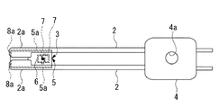
本実施形態の温度センサ1は、図1に示すように、一対のリードフレーム2と、一対のリードフレーム2に接続されたセンサ部3と、一対のリードフレーム2に固定されて一対のリードフレーム2を保持する絶縁性の保持部4とを備えている。
As shown in FIG. 1, the temperature sensor 1 according to the present embodiment includes a pair of
上記センサ部3は、上面に一対のリードフレーム2が接着された絶縁性フィルム5と、該絶縁性フィルム5の上面にサーミスタ材料でパターン形成された薄膜サーミスタ部6と、薄膜サーミスタ部6の上に複数の櫛部7aを有して互いに対向してパターン形成された一対の櫛型電極7と、一端が一対の櫛型電極7に接続されていると共に他端が一対のリードフレーム2に接続され絶縁性フィルム5の上面にパターン形成された一対のパターン電極8と、一対のリードフレーム2とセンサ部3とを上下から挟んで互いに接着された一対の絶縁性の保護テープ9A,9Bとを備えている。
The sensor unit 3 includes an
上記絶縁性フィルム5の両側部5aは、一対のリードフレーム2の接着面側に配された外側角部2bの近傍かつ内側に配されている。すなわち、絶縁性フィルム5の幅は、一対のリードフレーム2の外側角部2b間の距離よりも若干小さく設定されている。
また、一対の保護テープ9A,9Bの両側部9aは、絶縁性フィルム5の両側部5aから外側で上面側に向けて曲げられている。すなわち、一対の保護テープ9A,9Bは、その幅が一対のリードフレーム2の幅よりも広く設定され、絶縁性フィルム5の両側部5aに沿って谷折り状に折り曲げられている。
なお、両側部から中央部に向かう引っ張り力を付加された状態の上面側の保護テープ9Aを、下面側の保護テープ9Bに接着することで、上記折り曲げ状態を保持している。
Both
Further, both
Note that the bent state is maintained by adhering the
一対のリードフレーム2の先端部2aは、薄膜サーミスタ部6よりも先端側でパターン電極8と接続されていると共に、基端側に比べて互いに内側に幅広な形状とされている。
一対の上記パターン電極8の先端側には、リードフレーム2の先端部2aに対応して幅広なパッド部8aが形成されている。これらのパッド部8aに、一対のリードフレーム2が、ハンダ材や導電性樹脂接着剤等の接着剤、抵抗溶接により接着されている。
なお、本実施形態の温度センサ1では、パッド部8aを除いたパターン電極8,薄膜サーミスタ部6及び櫛型電極7を覆う絶縁性の保護膜10が絶縁性フィルム5上に形成されている。
The
A
In the temperature sensor 1 of the present embodiment, an insulating
上記絶縁性フィルム5は、略長方形状とされ、例えば厚さ7.5〜125μmのポリイミド樹脂シートで帯状に形成されている。なお、絶縁性フィルム5としては、他にPET:ポリエチレンテレフタレート,PEN:ポリエチレンナフタレート等でも作製できるが、加熱ローラの温度測定用としては、最高使用温度が230℃と高いためポリイミドフィルムが望ましい。
The said insulating
上記薄膜サーミスタ部6は、絶縁性フィルム5の基端側に配され、例えばTiAlNのサーミスタ材料で形成されている。特に、薄膜サーミスタ部6は、一般式:TixAlyNz(0.70≦y/(x+y)≦0.95、0.4≦z≦0.5、x+y+z=1)で示される金属窒化物からなり、その結晶構造が、六方晶系のウルツ鉱型の単相である。
The thin
上記パターン電極8及び櫛型電極7は、薄膜サーミスタ部6上に形成された膜厚5〜100nmのCr又はNiCrの接合層と、該接合層上にAu等の貴金属で膜厚50〜1000nmで形成された電極層とを有している。
一対の櫛型電極7は、互いに対向状態に配されて交互に櫛部7aが並んだ櫛型パターンとされている。
The
The pair of comb-shaped
なお、櫛部7aは、絶縁性フィルム5の延在方向に沿って延在している。すなわち、絶縁性フィルム5の裏面側を、回転する加熱ローラに押し当てされて温度測定を行う場合、絶縁性フィルム5の延在方向に曲率を有して湾曲させられるため、薄膜サーミスタ部6にも同方向に曲げ応力が加わる。このとき、櫛部7aが同方向に延在しているため、薄膜サーミスタ部6を補強することになり、クラックの発生を抑制することができる。
上記保護膜10は、絶縁性樹脂膜等であり、例えば厚さ20μmのポリイミド膜が採用される。
上記保護テープ9A,9Bは、テフロン(登録商標)等のフッ化炭素樹脂で形成されている。
なお、保持部4には、取付孔4aが形成されている。
The
The
The
The holding portion 4 has a mounting
この温度センサ1の製造方法について、図1から図4を参照して以下に説明する。
本実施形態の温度センサ1の製造方法は、絶縁性フィルム5の表面に薄膜サーミスタ部6をパターン形成する薄膜サーミスタ部形成工程と、互いに対向した一対の櫛型電極7を薄膜サーミスタ部6上に配して絶縁性フィルム5の表面に一対のパターン電極8をパターン形成する電極形成工程と、絶縁性フィルム5上に保護膜10を形成する保護膜形成工程と、センサ部3にリードフレーム2を接続するリードフレーム接続工程と、リードフレーム2及びセンサ部3を上下から保護テープ9A,9Bで挟んで互いに接着する保護テープ接着工程とを有している。
A method for manufacturing the temperature sensor 1 will be described below with reference to FIGS.
The manufacturing method of the temperature sensor 1 of the present embodiment includes a thin film thermistor portion forming step of patterning the thin
より具体的な製造方法の例としては、厚さ50μmのポリイミドフィルムの絶縁性フィルム5上に、Ti−Al合金スパッタリングターゲットを用い、窒素含有雰囲気中で反応性スパッタ法にて、TixAlyNz(x=0.09、y=0.43、z=0.48)のサーミスタ膜を膜厚200nmで形成する。その時のスパッタ条件は、到達真空度5×10⁻⁶Pa、スパッタガス圧0.4Pa、ターゲット投入電力(出力)200Wで、Arガス+窒素ガスの混合ガス雰囲気下において、窒素ガス分率を20%で作製する。
As a more specific example of the manufacturing method, Ti x Al y is used by reactive sputtering in a nitrogen-containing atmosphere using a Ti—Al alloy sputtering target on an insulating
成膜したサーミスタ膜の上にレジスト液をスピンコーターで塗布した後、110℃で1分30秒プリベークを行い、露光装置で感光後、現像液で不要部分を除去し、さらに150℃で5分のポストベークにてパターニングを行う。その後、不要なTixAlyNzのサーミスタ膜を市販のTiエッチャントでウェットエッチングを行い、図3の(a)に示すように、レジスト剥離にて所望の形状の薄膜サーミスタ部6にする。
A resist solution is applied onto the formed thermistor film by a spin coater, pre-baked at 110 ° C. for 1 minute 30 seconds, exposed to light with an exposure device, and unnecessary portions are removed with a developer, and further at 150 ° C. for 5 minutes. Patterning is performed by post-baking. Thereafter, the thermistor film unnecessary Ti x Al y N z by wet etching in a commercial Ti etchant, as shown in FIG. 3 (a), to a thin
次に、薄膜サーミスタ部6及び絶縁性フィルム5上に、スパッタ法にて、Cr膜の接合層を膜厚20nm形成する。さらに、この接合層上に、スパッタ法にてAu膜の電極層を膜厚200nm形成する。
次に、成膜した電極層の上にレジスト液をスピンコーターで塗布した後、110℃で1分30秒プリベークを行い、露光装置で感光後、現像液で不要部分を除去し、150℃で5分のポストベークにてパターニングを行う。その後、不要な電極部分を市販のAuエッチャント及びCrエッチャントの順番でウェットエッチングを行い、図3の(b)に示すように、レジスト剥離にて所望の櫛型電極7及びパターン電極8を形成する。
Next, a 20-nm-thick Cr film bonding layer is formed on the thin
Next, after applying a resist solution on the electrode layer formed by a spin coater, pre-baking is performed at 110 ° C. for 1 minute and 30 seconds, and after exposure with an exposure apparatus, unnecessary portions are removed with a developer, and at 150 ° C. Patterning is performed by post-baking for 5 minutes. Thereafter, unnecessary electrode portions are wet-etched in the order of a commercially available Au etchant and a Cr etchant, and as shown in FIG. 3B, desired
さらに、絶縁性フィルム5の表面にポリイミドワニスを印刷法により所定部分に塗布して、180℃、30分でキュアを行い、20μm厚のポリイミド保護膜10を形成する。
次に、パッド部8aとなる領域にNiめっきを施して、図2に示すように、一対のパッド部8aを形成する。
なお、複数のセンサ部3を同時に作製する場合、絶縁性フィルム2の大判シートに複数の薄膜サーミスタ部6、櫛型電極7、パターン電極7、保護膜10及びパッド部8aを上述のように形成した後に、大判シートから各センサ部3に切断する。
次に、図4に示すように、一対のパッド部8aにリードフレーム2の先端部2aを抵抗溶接により接着する。
Further, a polyimide varnish is applied to a predetermined portion on the surface of the insulating
Next, Ni plating is applied to a region to be the
When a plurality of sensor units 3 are manufactured simultaneously, a plurality of thin
Next, as shown in FIG. 4, the
さらに、センサ部3及びリードフレーム2を上下から一対の保護テープ9A,9Bで挟んで、一対の保護テープ9A,9Bの互いの両側部9aの接着面をプレスして接着する。この際、上面側の保護テープ9Aを、両側部から中央部に向かう引っ張り力を付加された状態で、下面側の保護テープ9Bに接着する。これにより、図1の(b)に示すように、下面側の保護テープ9Bが上面側の保護テープ9Aによって内側に引っ張られることで、一対の保護テープ9A,9Bの両側部9aが、絶縁性フィルム5の両側部5aから外側で上面側に向けて曲がり、温度センサ1が作製される。
Further, the sensor unit 3 and the
このように本実施形態の温度センサ1では、絶縁性フィルム5の両側部5aが、一対のリードフレーム2の接着面側に配された外側角部2bの近傍かつ内側に配され、一対の保護テープ9A,9Bの両側部9aが、絶縁性フィルム5の両側部5aから外側で上面側に向けて曲げられているので、リードフレーム2の外側角部2bが測定対象物に当接し難く、幅が狭い絶縁性フィルム5によって良好な応答性が得られる。
As described above, in the temperature sensor 1 of the present embodiment, the both
すなわち、リードフレーム2の外側角部2bの近傍内側に配された絶縁性フィルム5の両側部5aにより外側角部2b近傍に段差ができ、この段差より外側で曲がる保護テープ9A,9Bとリードフレーム2との間にわずかな隙間が生じることで、測定対象物に下面側の保護テープ9Bの下面を当接させた際に、外側角部2bが配された部分が測定対象物に当たり難くなって傷が発生し難い。
That is, a step is formed in the vicinity of the
また、幅が狭い絶縁性フィルム5と上記段差とによって保護テープ9A,9Bの両側部9aが一対のリードフレーム2の外側角部2bよりも内側から曲げられ、測定対象物との接触面が小さくなり、応答性が向上する。さらに、絶縁性フィルム5がリードフレーム2の外側角部2bよりも内側に配される狭い幅であることで、熱容量が小さく、良好な応答性を得ることができる。また、一対の保護テープ9A,9Bの両側部が上面側に向けて曲げられているので、一対の保護テープ9A,9Bの両側部9aが測定対象物に接触せず、一対の保護テープ9A,9Bの両側部9aによって測定対象物を傷つけることを防止できる。
Further, the both
また、上面側の保護テープ9Aが、両側部9aから中央部に向かう引っ張り力を付加された状態で、下面側の保護テープ9Bに接着されているので、上面側の保護テープ9Aの引っ張り力によって、貼り合わせた上下の保護テープ9A,9Bが絶縁性フィルム5の両側部5aの外側で上方に向けて曲がって、その形状が保持される。
さらに、一対のリードフレーム2の先端部2aが、薄膜サーミスタ部6よりも先端側でパターン電極8と接続されていると共に、基端側に比べて互いに内側に幅広な形状とされているので、外側角部2bよりも内側に配されて接着面積が小さくなった絶縁性フィルム5との接着面積を幅広な先端部5aで増やし、センサ部3を平坦かつ安定的に保持することができる。なお、リードフレーム2の先端部2aは、薄膜サーミスタ部6よりも先端側に配されてパターン電極8に接続されるので、先端部2aを内側に幅広にしても薄膜サーミスタ部6の領域を狭めることがない。
In addition, since the upper surface side
Further, the
なお、本発明の技術範囲は上記実施形態に限定されるものではなく、本発明の趣旨を逸脱しない範囲において種々の変更を加えることが可能である。 The technical scope of the present invention is not limited to the above embodiment, and various modifications can be made without departing from the spirit of the present invention.
1…温度センサ、2…リードフレーム、2b…リードフレームの外側角部、3…センサ部、4…保持部、5…絶縁性フィルム、5a…絶縁性フィルムの両側部、6…薄膜サーミスタ部、7…櫛型電極、7a…櫛部、8…パターン電極、9A,9B…保護テープ、9a…保護テープの両側部 DESCRIPTION OF SYMBOLS 1 ... Temperature sensor, 2 ... Lead frame, 2b ... Outer corner part of lead frame, 3 ... Sensor part, 4 ... Holding part, 5 ... Insulating film, 5a ... Both sides of insulating film, 6 ... Thin film thermistor part, 7 ... Comb electrode, 7a ... Comb, 8 ... Pattern electrode, 9A, 9B ... Protection tape, 9a ... Both sides of protection tape
Claims (4)
前記センサ部が、上面に前記一対のリードフレームが接着された絶縁性フィルムと、
該絶縁性フィルムの上面に設けられサーミスタ材料で形成されたサーミスタ部と、
前記サーミスタ部に互いに対向して形成された一対の電極と、
一端が前記一対の電極に接続されていると共に他端が前記一対のリードフレームに接続され前記絶縁性フィルムの上面にパターン形成された一対のパターン電極とを備え、
前記絶縁性フィルムの両側部が、前記一対のリードフレームの接着面側に配された外側角部の近傍かつ内側に配され、
一対の前記保護テープの両側部が、前記絶縁性フィルムの両側部から外側で、かつ前記一対のリードフレームの外側角部よりも内側から上面側に向けて曲げられていることを特徴とする温度センサ。 A pair of lead frames; a sensor portion connected to the pair of lead frames; a pair of insulating protective tapes that are bonded to each other with the pair of lead frames and the sensor portion sandwiched from above and below ; An insulating holding part fixed to the lead frame and holding the pair of lead frames,
The sensor part is an insulating film having the pair of lead frames bonded to the upper surface;
A thermistor portion formed of the thermistor material provided on the upper surface of the insulating film;
A pair of electrodes formed opposite to each other on the thermistor portion;
One end and a pair of pattern electrodes other end with being connected to the pair of electrodes are patterned on the upper surface of the insulating film connected to the pair of lead frames,
Both sides of the insulating film are arranged in the vicinity and inside of the outer corners arranged on the bonding surface side of the pair of lead frames,
A temperature characterized in that both sides of the pair of protective tapes are bent outward from both sides of the insulating film and from the inside to the upper side of the outer corners of the pair of lead frames. Sensor.
上面側の前記保護テープが、両側部から中央部に向かう引っ張り力を付加された状態で、下面側の前記保護テープに接着されていることを特徴とする温度センサ。 The temperature sensor according to claim 1,
The temperature sensor, wherein the protective tape on the upper surface side is bonded to the protective tape on the lower surface side in a state where a tensile force from both side portions toward the central portion is applied.
前記一対のリードフレームの先端部が、前記サーミスタ部よりも先端側で前記パターン電極と接続されていると共に、基端側に比べて互いに内側に幅広な形状とされていることを特徴とする温度センサ。 The temperature sensor according to claim 1 or 2,
The temperature is characterized in that the distal ends of the pair of lead frames are connected to the pattern electrode at the distal end side with respect to the thermistor portion, and have a shape wider inside than the proximal end side. Sensor.
前記サーミスタ部が、前記絶縁性フィルムの上面にサーミスタ材料でパターン形成された薄膜サーミスタ部であり、
前記一対の電極が、前記薄膜サーミスタ部の上及び下の少なくとも一方に複数の櫛部を有して互いに対向してパターン形成された一対の櫛型電極であることを特徴とする温度センサ。 The temperature sensor according to any one of claims 1 to 3,
The thermistor portion is a thin film thermistor portion patterned with a thermistor material on the upper surface of the insulating film,
2. The temperature sensor according to claim 1, wherein the pair of electrodes is a pair of comb-shaped electrodes having a plurality of comb portions on at least one of the upper and lower sides of the thin film thermistor portion and patterned to face each other.
Priority Applications (4)
| Application Number | Priority Date | Filing Date | Title |
|---|---|---|---|
| JP2015150529A JP6617909B2 (en) | 2015-07-30 | 2015-07-30 | Temperature sensor |
| CN201680044835.4A CN107923801A (en) | 2015-07-30 | 2016-07-11 | Temperature sensor |
| US15/748,202 US20180217007A1 (en) | 2015-07-30 | 2016-07-11 | Temperature sensor |
| PCT/JP2016/003272 WO2017017916A1 (en) | 2015-07-30 | 2016-07-11 | Temperature sensor |
Applications Claiming Priority (1)
| Application Number | Priority Date | Filing Date | Title |
|---|---|---|---|
| JP2015150529A JP6617909B2 (en) | 2015-07-30 | 2015-07-30 | Temperature sensor |
Publications (3)
| Publication Number | Publication Date |
|---|---|
| JP2017032336A JP2017032336A (en) | 2017-02-09 |
| JP2017032336A5 JP2017032336A5 (en) | 2017-12-28 |
| JP6617909B2 true JP6617909B2 (en) | 2019-12-11 |
Family
ID=57884337
Family Applications (1)
| Application Number | Title | Priority Date | Filing Date |
|---|---|---|---|
| JP2015150529A Active JP6617909B2 (en) | 2015-07-30 | 2015-07-30 | Temperature sensor |
Country Status (4)
| Country | Link |
|---|---|
| US (1) | US20180217007A1 (en) |
| JP (1) | JP6617909B2 (en) |
| CN (1) | CN107923801A (en) |
| WO (1) | WO2017017916A1 (en) |
Families Citing this family (2)
| Publication number | Priority date | Publication date | Assignee | Title |
|---|---|---|---|---|
| JP7293734B2 (en) * | 2019-03-06 | 2023-06-20 | 株式会社リコー | Fixing device and image forming device |
| JP2021047241A (en) * | 2019-09-17 | 2021-03-25 | 富士ゼロックス株式会社 | Fixation device and image formation apparatus |
Family Cites Families (6)
| Publication number | Priority date | Publication date | Assignee | Title |
|---|---|---|---|---|
| JP2505631Y2 (en) * | 1991-07-04 | 1996-07-31 | 石塚電子株式会社 | Temperature sensor |
| JP4838667B2 (en) * | 2006-09-01 | 2011-12-14 | キヤノン株式会社 | Temperature sensor and fixing device |
| JP5896157B2 (en) * | 2012-09-06 | 2016-03-30 | 三菱マテリアル株式会社 | Temperature sensor |
| JP6011285B2 (en) * | 2012-12-03 | 2016-10-19 | 三菱マテリアル株式会社 | Temperature sensor |
| JP6052614B2 (en) * | 2013-03-21 | 2016-12-27 | 三菱マテリアル株式会社 | Temperature sensor |
| JP5928831B2 (en) * | 2013-03-21 | 2016-06-01 | 三菱マテリアル株式会社 | Temperature sensor |
-
2015
- 2015-07-30 JP JP2015150529A patent/JP6617909B2/en active Active
-
2016
- 2016-07-11 US US15/748,202 patent/US20180217007A1/en not_active Abandoned
- 2016-07-11 WO PCT/JP2016/003272 patent/WO2017017916A1/en active Application Filing
- 2016-07-11 CN CN201680044835.4A patent/CN107923801A/en active Pending
Also Published As
| Publication number | Publication date |
|---|---|
| JP2017032336A (en) | 2017-02-09 |
| WO2017017916A1 (en) | 2017-02-02 |
| US20180217007A1 (en) | 2018-08-02 |
| CN107923801A (en) | 2018-04-17 |
Similar Documents
| Publication | Publication Date | Title |
|---|---|---|
| JP5316959B2 (en) | Thin film thermistor sensor | |
| JP5896157B2 (en) | Temperature sensor | |
| JP5928829B2 (en) | Temperature sensor | |
| JP6617909B2 (en) | Temperature sensor | |
| JP2012067502A (en) | Window glass having temperature sensor | |
| JP6052614B2 (en) | Temperature sensor | |
| JP2017053782A (en) | Temperature sensor | |
| JP6603991B2 (en) | Temperature sensor | |
| JP5652082B2 (en) | Electrolytic capacitor with temperature sensor | |
| JP6583073B2 (en) | Temperature sensor | |
| JP6256690B2 (en) | Non-contact temperature sensor | |
| JP2017166939A (en) | Temperature sensor | |
| JP6410048B2 (en) | Temperature sensor | |
| JP2017026415A (en) | Temperature sensor | |
| JP6460376B2 (en) | Temperature sensor and manufacturing method thereof | |
| JP2017072401A (en) | Temperature sensor | |
| JP6641770B2 (en) | Temperature sensor | |
| WO2017081832A1 (en) | Temperature sensor and method for manufacturing same | |
| JP6772843B2 (en) | Temperature sensor | |
| JP2016090262A (en) | Temperature sensor and manufacturing method thereof | |
| JP6410024B2 (en) | Temperature sensor | |
| JPH11354302A (en) | Thin-film resistor element | |
| JP2018132497A (en) | Temperature sensor | |
| JP2017161331A (en) | Temperature sensor and method of manufacturing the same | |
| JP2017096719A (en) | Temperature sensor and method of manufacturing the same |
Legal Events
| Date | Code | Title | Description |
|---|---|---|---|
| A521 | Request for written amendment filed |
Free format text: JAPANESE INTERMEDIATE CODE: A523 Effective date: 20171120 |
|
| A621 | Written request for application examination |
Free format text: JAPANESE INTERMEDIATE CODE: A621 Effective date: 20180327 |
|
| A131 | Notification of reasons for refusal |
Free format text: JAPANESE INTERMEDIATE CODE: A131 Effective date: 20190327 |
|
| A521 | Request for written amendment filed |
Free format text: JAPANESE INTERMEDIATE CODE: A523 Effective date: 20190508 |
|
| TRDD | Decision of grant or rejection written | ||
| A01 | Written decision to grant a patent or to grant a registration (utility model) |
Free format text: JAPANESE INTERMEDIATE CODE: A01 Effective date: 20191017 |
|
| A61 | First payment of annual fees (during grant procedure) |
Free format text: JAPANESE INTERMEDIATE CODE: A61 Effective date: 20191030 |
|
| R150 | Certificate of patent or registration of utility model |
Ref document number: 6617909 Country of ref document: JP Free format text: JAPANESE INTERMEDIATE CODE: R150 |