JP6503157B2 - 液晶表示装置 - Google Patents
液晶表示装置 Download PDFInfo
- Publication number
- JP6503157B2 JP6503157B2 JP2014054832A JP2014054832A JP6503157B2 JP 6503157 B2 JP6503157 B2 JP 6503157B2 JP 2014054832 A JP2014054832 A JP 2014054832A JP 2014054832 A JP2014054832 A JP 2014054832A JP 6503157 B2 JP6503157 B2 JP 6503157B2
- Authority
- JP
- Japan
- Prior art keywords
- electrode
- film
- liquid crystal
- transistor
- substrate
- Prior art date
- Legal status (The legal status is an assumption and is not a legal conclusion. Google has not performed a legal analysis and makes no representation as to the accuracy of the status listed.)
- Active
Links
- 239000004973 liquid crystal related substance Substances 0.000 title claims description 184
- 239000000758 substrate Substances 0.000 claims description 130
- 239000004065 semiconductor Substances 0.000 claims description 113
- 239000011347 resin Substances 0.000 claims description 49
- 229920005989 resin Polymers 0.000 claims description 49
- 230000015572 biosynthetic process Effects 0.000 claims description 44
- 230000005684 electric field Effects 0.000 claims description 13
- 239000010408 film Substances 0.000 description 593
- 229910044991 metal oxide Inorganic materials 0.000 description 62
- 150000004706 metal oxides Chemical class 0.000 description 62
- 239000010410 layer Substances 0.000 description 45
- 239000011701 zinc Substances 0.000 description 45
- 239000001301 oxygen Substances 0.000 description 41
- 229910052760 oxygen Inorganic materials 0.000 description 41
- QVGXLLKOCUKJST-UHFFFAOYSA-N atomic oxygen Chemical compound [O] QVGXLLKOCUKJST-UHFFFAOYSA-N 0.000 description 40
- 230000006870 function Effects 0.000 description 33
- 239000013078 crystal Substances 0.000 description 32
- 239000007789 gas Substances 0.000 description 25
- 239000004020 conductor Substances 0.000 description 22
- XUIMIQQOPSSXEZ-UHFFFAOYSA-N Silicon Chemical compound [Si] XUIMIQQOPSSXEZ-UHFFFAOYSA-N 0.000 description 20
- 238000000034 method Methods 0.000 description 20
- 229910052710 silicon Inorganic materials 0.000 description 20
- 239000010703 silicon Substances 0.000 description 20
- 229910052751 metal Inorganic materials 0.000 description 19
- VYPSYNLAJGMNEJ-UHFFFAOYSA-N Silicium dioxide Chemical compound O=[Si]=O VYPSYNLAJGMNEJ-UHFFFAOYSA-N 0.000 description 18
- XLOMVQKBTHCTTD-UHFFFAOYSA-N Zinc monoxide Chemical compound [Zn]=O XLOMVQKBTHCTTD-UHFFFAOYSA-N 0.000 description 18
- 239000012535 impurity Substances 0.000 description 16
- 229910052814 silicon oxide Inorganic materials 0.000 description 16
- 239000002184 metal Substances 0.000 description 15
- 238000012545 processing Methods 0.000 description 15
- 238000004519 manufacturing process Methods 0.000 description 13
- 230000008859 change Effects 0.000 description 12
- 239000001257 hydrogen Substances 0.000 description 12
- 229910052739 hydrogen Inorganic materials 0.000 description 12
- 229910052738 indium Inorganic materials 0.000 description 12
- 238000004544 sputter deposition Methods 0.000 description 12
- 239000003990 capacitor Substances 0.000 description 11
- 238000010438 heat treatment Methods 0.000 description 11
- AMGQUBHHOARCQH-UHFFFAOYSA-N indium;oxotin Chemical compound [In].[Sn]=O AMGQUBHHOARCQH-UHFFFAOYSA-N 0.000 description 11
- 239000002245 particle Substances 0.000 description 11
- 230000015654 memory Effects 0.000 description 10
- 229910052581 Si3N4 Inorganic materials 0.000 description 9
- GWEVSGVZZGPLCZ-UHFFFAOYSA-N Titan oxide Chemical compound O=[Ti]=O GWEVSGVZZGPLCZ-UHFFFAOYSA-N 0.000 description 9
- HQVNEWCFYHHQES-UHFFFAOYSA-N silicon nitride Chemical compound N12[Si]34N5[Si]62N3[Si]51N64 HQVNEWCFYHHQES-UHFFFAOYSA-N 0.000 description 9
- 239000011787 zinc oxide Substances 0.000 description 9
- 229910052733 gallium Inorganic materials 0.000 description 8
- APFVFJFRJDLVQX-UHFFFAOYSA-N indium atom Chemical compound [In] APFVFJFRJDLVQX-UHFFFAOYSA-N 0.000 description 8
- 238000005268 plasma chemical vapour deposition Methods 0.000 description 8
- 238000002834 transmittance Methods 0.000 description 8
- UFHFLCQGNIYNRP-UHFFFAOYSA-N Hydrogen Chemical compound [H][H] UFHFLCQGNIYNRP-UHFFFAOYSA-N 0.000 description 7
- 238000005530 etching Methods 0.000 description 7
- 229910003437 indium oxide Inorganic materials 0.000 description 7
- PJXISJQVUVHSOJ-UHFFFAOYSA-N indium(iii) oxide Chemical compound [O-2].[O-2].[O-2].[In+3].[In+3] PJXISJQVUVHSOJ-UHFFFAOYSA-N 0.000 description 7
- 230000003071 parasitic effect Effects 0.000 description 7
- 239000000843 powder Substances 0.000 description 7
- OGIDPMRJRNCKJF-UHFFFAOYSA-N titanium oxide Inorganic materials [Ti]=O OGIDPMRJRNCKJF-UHFFFAOYSA-N 0.000 description 7
- XKRFYHLGVUSROY-UHFFFAOYSA-N Argon Chemical compound [Ar] XKRFYHLGVUSROY-UHFFFAOYSA-N 0.000 description 6
- GQPLMRYTRLFLPF-UHFFFAOYSA-N Nitrous Oxide Chemical compound [O-][N+]#N GQPLMRYTRLFLPF-UHFFFAOYSA-N 0.000 description 6
- 229910052782 aluminium Inorganic materials 0.000 description 6
- 125000004429 atom Chemical group 0.000 description 6
- 238000000151 deposition Methods 0.000 description 6
- 230000008021 deposition Effects 0.000 description 6
- QGLKJKCYBOYXKC-UHFFFAOYSA-N nonaoxidotritungsten Chemical compound O=[W]1(=O)O[W](=O)(=O)O[W](=O)(=O)O1 QGLKJKCYBOYXKC-UHFFFAOYSA-N 0.000 description 6
- 239000003381 stabilizer Substances 0.000 description 6
- 229910001930 tungsten oxide Inorganic materials 0.000 description 6
- XLYOFNOQVPJJNP-UHFFFAOYSA-N water Substances O XLYOFNOQVPJJNP-UHFFFAOYSA-N 0.000 description 6
- 229910001868 water Inorganic materials 0.000 description 6
- YVTHLONGBIQYBO-UHFFFAOYSA-N zinc indium(3+) oxygen(2-) Chemical compound [O--].[Zn++].[In+3] YVTHLONGBIQYBO-UHFFFAOYSA-N 0.000 description 6
- 208000005156 Dehydration Diseases 0.000 description 5
- GYHNNYVSQQEPJS-UHFFFAOYSA-N Gallium Chemical compound [Ga] GYHNNYVSQQEPJS-UHFFFAOYSA-N 0.000 description 5
- 229910020994 Sn-Zn Inorganic materials 0.000 description 5
- 229910009069 Sn—Zn Inorganic materials 0.000 description 5
- 238000004458 analytical method Methods 0.000 description 5
- 230000018044 dehydration Effects 0.000 description 5
- 238000006297 dehydration reaction Methods 0.000 description 5
- 238000006356 dehydrogenation reaction Methods 0.000 description 5
- 150000002431 hydrogen Chemical class 0.000 description 5
- 239000000463 material Substances 0.000 description 5
- 239000011734 sodium Substances 0.000 description 5
- 229910052719 titanium Inorganic materials 0.000 description 5
- 239000010936 titanium Substances 0.000 description 5
- 229910052721 tungsten Inorganic materials 0.000 description 5
- QGZKDVFQNNGYKY-UHFFFAOYSA-N Ammonia Chemical compound N QGZKDVFQNNGYKY-UHFFFAOYSA-N 0.000 description 4
- OKTJSMMVPCPJKN-UHFFFAOYSA-N Carbon Chemical compound [C] OKTJSMMVPCPJKN-UHFFFAOYSA-N 0.000 description 4
- 230000000903 blocking effect Effects 0.000 description 4
- 229910052799 carbon Inorganic materials 0.000 description 4
- 229910052804 chromium Inorganic materials 0.000 description 4
- 239000011651 chromium Substances 0.000 description 4
- 229910052802 copper Inorganic materials 0.000 description 4
- 239000010949 copper Substances 0.000 description 4
- 230000007547 defect Effects 0.000 description 4
- AJNVQOSZGJRYEI-UHFFFAOYSA-N digallium;oxygen(2-) Chemical compound [O-2].[O-2].[O-2].[Ga+3].[Ga+3] AJNVQOSZGJRYEI-UHFFFAOYSA-N 0.000 description 4
- 229910001195 gallium oxide Inorganic materials 0.000 description 4
- 239000011521 glass Substances 0.000 description 4
- 239000000203 mixture Substances 0.000 description 4
- 230000004044 response Effects 0.000 description 4
- 239000003566 sealing material Substances 0.000 description 4
- 229910052725 zinc Inorganic materials 0.000 description 4
- 229910018137 Al-Zn Inorganic materials 0.000 description 3
- 229910018573 Al—Zn Inorganic materials 0.000 description 3
- 229910052684 Cerium Inorganic materials 0.000 description 3
- MYMOFIZGZYHOMD-UHFFFAOYSA-N Dioxygen Chemical compound O=O MYMOFIZGZYHOMD-UHFFFAOYSA-N 0.000 description 3
- 206010021143 Hypoxia Diseases 0.000 description 3
- PXHVJJICTQNCMI-UHFFFAOYSA-N Nickel Chemical compound [Ni] PXHVJJICTQNCMI-UHFFFAOYSA-N 0.000 description 3
- BLRPTPMANUNPDV-UHFFFAOYSA-N Silane Chemical compound [SiH4] BLRPTPMANUNPDV-UHFFFAOYSA-N 0.000 description 3
- 230000002411 adverse Effects 0.000 description 3
- 229910052783 alkali metal Inorganic materials 0.000 description 3
- 150000001340 alkali metals Chemical class 0.000 description 3
- XAGFODPZIPBFFR-UHFFFAOYSA-N aluminium Chemical compound [Al] XAGFODPZIPBFFR-UHFFFAOYSA-N 0.000 description 3
- 229910052786 argon Inorganic materials 0.000 description 3
- 239000000969 carrier Substances 0.000 description 3
- 230000006866 deterioration Effects 0.000 description 3
- 229910001882 dioxygen Inorganic materials 0.000 description 3
- 229910052735 hafnium Inorganic materials 0.000 description 3
- 229910052746 lanthanum Inorganic materials 0.000 description 3
- 229910052750 molybdenum Inorganic materials 0.000 description 3
- 229960001730 nitrous oxide Drugs 0.000 description 3
- 235000013842 nitrous oxide Nutrition 0.000 description 3
- 230000001590 oxidative effect Effects 0.000 description 3
- 229910000077 silane Inorganic materials 0.000 description 3
- 229910052715 tantalum Inorganic materials 0.000 description 3
- 229910052718 tin Inorganic materials 0.000 description 3
- 239000010937 tungsten Substances 0.000 description 3
- 229910052726 zirconium Inorganic materials 0.000 description 3
- 229910018120 Al-Ga-Zn Inorganic materials 0.000 description 2
- IJGRMHOSHXDMSA-UHFFFAOYSA-N Atomic nitrogen Chemical compound N#N IJGRMHOSHXDMSA-UHFFFAOYSA-N 0.000 description 2
- CURLTUGMZLYLDI-UHFFFAOYSA-N Carbon dioxide Chemical compound O=C=O CURLTUGMZLYLDI-UHFFFAOYSA-N 0.000 description 2
- VYZAMTAEIAYCRO-UHFFFAOYSA-N Chromium Chemical compound [Cr] VYZAMTAEIAYCRO-UHFFFAOYSA-N 0.000 description 2
- RYGMFSIKBFXOCR-UHFFFAOYSA-N Copper Chemical compound [Cu] RYGMFSIKBFXOCR-UHFFFAOYSA-N 0.000 description 2
- 238000004435 EPR spectroscopy Methods 0.000 description 2
- 229910002601 GaN Inorganic materials 0.000 description 2
- JMASRVWKEDWRBT-UHFFFAOYSA-N Gallium nitride Chemical compound [Ga]#N JMASRVWKEDWRBT-UHFFFAOYSA-N 0.000 description 2
- 229910052779 Neodymium Inorganic materials 0.000 description 2
- 229910020833 Sn-Al-Zn Inorganic materials 0.000 description 2
- 229910020868 Sn-Ga-Zn Inorganic materials 0.000 description 2
- ATJFFYVFTNAWJD-UHFFFAOYSA-N Tin Chemical compound [Sn] ATJFFYVFTNAWJD-UHFFFAOYSA-N 0.000 description 2
- RTAQQCXQSZGOHL-UHFFFAOYSA-N Titanium Chemical compound [Ti] RTAQQCXQSZGOHL-UHFFFAOYSA-N 0.000 description 2
- QCWXUUIWCKQGHC-UHFFFAOYSA-N Zirconium Chemical compound [Zr] QCWXUUIWCKQGHC-UHFFFAOYSA-N 0.000 description 2
- NIXOWILDQLNWCW-UHFFFAOYSA-N acrylic acid group Chemical group C(C=C)(=O)O NIXOWILDQLNWCW-UHFFFAOYSA-N 0.000 description 2
- 229910052784 alkaline earth metal Inorganic materials 0.000 description 2
- 150000001342 alkaline earth metals Chemical class 0.000 description 2
- 229910021529 ammonia Inorganic materials 0.000 description 2
- GWXLDORMOJMVQZ-UHFFFAOYSA-N cerium Chemical compound [Ce] GWXLDORMOJMVQZ-UHFFFAOYSA-N 0.000 description 2
- 230000000694 effects Effects 0.000 description 2
- 238000000605 extraction Methods 0.000 description 2
- 230000005669 field effect Effects 0.000 description 2
- 229910052732 germanium Inorganic materials 0.000 description 2
- GNPVGFCGXDBREM-UHFFFAOYSA-N germanium atom Chemical compound [Ge] GNPVGFCGXDBREM-UHFFFAOYSA-N 0.000 description 2
- VBJZVLUMGGDVMO-UHFFFAOYSA-N hafnium atom Chemical compound [Hf] VBJZVLUMGGDVMO-UHFFFAOYSA-N 0.000 description 2
- 230000001788 irregular Effects 0.000 description 2
- FZLIPJUXYLNCLC-UHFFFAOYSA-N lanthanum atom Chemical compound [La] FZLIPJUXYLNCLC-UHFFFAOYSA-N 0.000 description 2
- MRELNEQAGSRDBK-UHFFFAOYSA-N lanthanum(3+);oxygen(2-) Chemical compound [O-2].[O-2].[O-2].[La+3].[La+3] MRELNEQAGSRDBK-UHFFFAOYSA-N 0.000 description 2
- 238000005259 measurement Methods 0.000 description 2
- 230000005012 migration Effects 0.000 description 2
- 238000013508 migration Methods 0.000 description 2
- 238000002156 mixing Methods 0.000 description 2
- PLDDOISOJJCEMH-UHFFFAOYSA-N neodymium(3+);oxygen(2-) Chemical compound [O-2].[O-2].[O-2].[Nd+3].[Nd+3] PLDDOISOJJCEMH-UHFFFAOYSA-N 0.000 description 2
- 229910052759 nickel Inorganic materials 0.000 description 2
- 150000004767 nitrides Chemical class 0.000 description 2
- 230000003647 oxidation Effects 0.000 description 2
- 238000007254 oxidation reaction Methods 0.000 description 2
- SIWVEOZUMHYXCS-UHFFFAOYSA-N oxo(oxoyttriooxy)yttrium Chemical compound O=[Y]O[Y]=O SIWVEOZUMHYXCS-UHFFFAOYSA-N 0.000 description 2
- 239000004033 plastic Substances 0.000 description 2
- 229920003023 plastic Polymers 0.000 description 2
- 229920001721 polyimide Polymers 0.000 description 2
- 238000003825 pressing Methods 0.000 description 2
- 239000010453 quartz Substances 0.000 description 2
- 238000001004 secondary ion mass spectrometry Methods 0.000 description 2
- 229910010271 silicon carbide Inorganic materials 0.000 description 2
- HBMJWWWQQXIZIP-UHFFFAOYSA-N silicon carbide Chemical compound [Si+]#[C-] HBMJWWWQQXIZIP-UHFFFAOYSA-N 0.000 description 2
- 239000002356 single layer Substances 0.000 description 2
- 230000003068 static effect Effects 0.000 description 2
- WFKWXMTUELFFGS-UHFFFAOYSA-N tungsten Chemical compound [W] WFKWXMTUELFFGS-UHFFFAOYSA-N 0.000 description 2
- -1 tungsten nitride Chemical class 0.000 description 2
- 229910052727 yttrium Inorganic materials 0.000 description 2
- VWQVUPCCIRVNHF-UHFFFAOYSA-N yttrium atom Chemical compound [Y] VWQVUPCCIRVNHF-UHFFFAOYSA-N 0.000 description 2
- MGWGWNFMUOTEHG-UHFFFAOYSA-N 4-(3,5-dimethylphenyl)-1,3-thiazol-2-amine Chemical compound CC1=CC(C)=CC(C=2N=C(N)SC=2)=C1 MGWGWNFMUOTEHG-UHFFFAOYSA-N 0.000 description 1
- 239000004925 Acrylic resin Substances 0.000 description 1
- 229920000178 Acrylic resin Polymers 0.000 description 1
- 229910052692 Dysprosium Inorganic materials 0.000 description 1
- 229910052691 Erbium Inorganic materials 0.000 description 1
- 229910052693 Europium Inorganic materials 0.000 description 1
- 229910052688 Gadolinium Inorganic materials 0.000 description 1
- 229910052689 Holmium Inorganic materials 0.000 description 1
- DGAQECJNVWCQMB-PUAWFVPOSA-M Ilexoside XXIX Chemical compound C[C@@H]1CC[C@@]2(CC[C@@]3(C(=CC[C@H]4[C@]3(CC[C@@H]5[C@@]4(CC[C@@H](C5(C)C)OS(=O)(=O)[O-])C)C)[C@@H]2[C@]1(C)O)C)C(=O)O[C@H]6[C@@H]([C@H]([C@@H]([C@H](O6)CO)O)O)O.[Na+] DGAQECJNVWCQMB-PUAWFVPOSA-M 0.000 description 1
- WHXSMMKQMYFTQS-UHFFFAOYSA-N Lithium Chemical compound [Li] WHXSMMKQMYFTQS-UHFFFAOYSA-N 0.000 description 1
- 229910052765 Lutetium Inorganic materials 0.000 description 1
- ZOKXTWBITQBERF-UHFFFAOYSA-N Molybdenum Chemical compound [Mo] ZOKXTWBITQBERF-UHFFFAOYSA-N 0.000 description 1
- 239000004677 Nylon Substances 0.000 description 1
- CBENFWSGALASAD-UHFFFAOYSA-N Ozone Chemical compound [O-][O+]=O CBENFWSGALASAD-UHFFFAOYSA-N 0.000 description 1
- 239000004642 Polyimide Substances 0.000 description 1
- 239000004372 Polyvinyl alcohol Substances 0.000 description 1
- ZLMJMSJWJFRBEC-UHFFFAOYSA-N Potassium Chemical compound [K] ZLMJMSJWJFRBEC-UHFFFAOYSA-N 0.000 description 1
- 229910052777 Praseodymium Inorganic materials 0.000 description 1
- KJTLSVCANCCWHF-UHFFFAOYSA-N Ruthenium Chemical compound [Ru] KJTLSVCANCCWHF-UHFFFAOYSA-N 0.000 description 1
- 229910052772 Samarium Inorganic materials 0.000 description 1
- BQCADISMDOOEFD-UHFFFAOYSA-N Silver Chemical compound [Ag] BQCADISMDOOEFD-UHFFFAOYSA-N 0.000 description 1
- 229910020944 Sn-Mg Inorganic materials 0.000 description 1
- 229910052771 Terbium Inorganic materials 0.000 description 1
- 229910052775 Thulium Inorganic materials 0.000 description 1
- 238000002441 X-ray diffraction Methods 0.000 description 1
- 229910052769 Ytterbium Inorganic materials 0.000 description 1
- 229910009369 Zn Mg Inorganic materials 0.000 description 1
- 229910007573 Zn-Mg Inorganic materials 0.000 description 1
- 238000013459 approach Methods 0.000 description 1
- 239000002585 base Substances 0.000 description 1
- 230000008901 benefit Effects 0.000 description 1
- 230000005540 biological transmission Effects 0.000 description 1
- 239000006229 carbon black Substances 0.000 description 1
- 239000001569 carbon dioxide Substances 0.000 description 1
- 229910002092 carbon dioxide Inorganic materials 0.000 description 1
- 239000000919 ceramic Substances 0.000 description 1
- 239000011248 coating agent Substances 0.000 description 1
- 238000000576 coating method Methods 0.000 description 1
- 229910017052 cobalt Inorganic materials 0.000 description 1
- 239000010941 cobalt Substances 0.000 description 1
- GUTLYIVDDKVIGB-UHFFFAOYSA-N cobalt atom Chemical compound [Co] GUTLYIVDDKVIGB-UHFFFAOYSA-N 0.000 description 1
- 238000002425 crystallisation Methods 0.000 description 1
- 230000008025 crystallization Effects 0.000 description 1
- 238000000354 decomposition reaction Methods 0.000 description 1
- 238000003795 desorption Methods 0.000 description 1
- 238000010586 diagram Methods 0.000 description 1
- PZPGRFITIJYNEJ-UHFFFAOYSA-N disilane Chemical compound [SiH3][SiH3] PZPGRFITIJYNEJ-UHFFFAOYSA-N 0.000 description 1
- 238000009826 distribution Methods 0.000 description 1
- KBQHZAAAGSGFKK-UHFFFAOYSA-N dysprosium atom Chemical compound [Dy] KBQHZAAAGSGFKK-UHFFFAOYSA-N 0.000 description 1
- 230000005611 electricity Effects 0.000 description 1
- UYAHIZSMUZPPFV-UHFFFAOYSA-N erbium Chemical compound [Er] UYAHIZSMUZPPFV-UHFFFAOYSA-N 0.000 description 1
- OGPBJKLSAFTDLK-UHFFFAOYSA-N europium atom Chemical compound [Eu] OGPBJKLSAFTDLK-UHFFFAOYSA-N 0.000 description 1
- 238000002474 experimental method Methods 0.000 description 1
- 239000004744 fabric Substances 0.000 description 1
- XPBBUZJBQWWFFJ-UHFFFAOYSA-N fluorosilane Chemical compound [SiH3]F XPBBUZJBQWWFFJ-UHFFFAOYSA-N 0.000 description 1
- UIWYJDYFSGRHKR-UHFFFAOYSA-N gadolinium atom Chemical compound [Gd] UIWYJDYFSGRHKR-UHFFFAOYSA-N 0.000 description 1
- YBMRDBCBODYGJE-UHFFFAOYSA-N germanium oxide Inorganic materials O=[Ge]=O YBMRDBCBODYGJE-UHFFFAOYSA-N 0.000 description 1
- 229910052737 gold Inorganic materials 0.000 description 1
- 229910000449 hafnium oxide Inorganic materials 0.000 description 1
- WIHZLLGSGQNAGK-UHFFFAOYSA-N hafnium(4+);oxygen(2-) Chemical compound [O-2].[O-2].[Hf+4] WIHZLLGSGQNAGK-UHFFFAOYSA-N 0.000 description 1
- KJZYNXUDTRRSPN-UHFFFAOYSA-N holmium atom Chemical compound [Ho] KJZYNXUDTRRSPN-UHFFFAOYSA-N 0.000 description 1
- 230000001771 impaired effect Effects 0.000 description 1
- 238000002347 injection Methods 0.000 description 1
- 239000007924 injection Substances 0.000 description 1
- 229910010272 inorganic material Inorganic materials 0.000 description 1
- 239000011147 inorganic material Substances 0.000 description 1
- 238000009413 insulation Methods 0.000 description 1
- 150000002500 ions Chemical class 0.000 description 1
- 238000010030 laminating Methods 0.000 description 1
- 229910052747 lanthanoid Inorganic materials 0.000 description 1
- 150000002602 lanthanoids Chemical class 0.000 description 1
- 229910052744 lithium Inorganic materials 0.000 description 1
- OHSVLFRHMCKCQY-UHFFFAOYSA-N lutetium atom Chemical compound [Lu] OHSVLFRHMCKCQY-UHFFFAOYSA-N 0.000 description 1
- 239000011777 magnesium Substances 0.000 description 1
- 239000000395 magnesium oxide Substances 0.000 description 1
- CPLXHLVBOLITMK-UHFFFAOYSA-N magnesium oxide Inorganic materials [Mg]=O CPLXHLVBOLITMK-UHFFFAOYSA-N 0.000 description 1
- AXZKOIWUVFPNLO-UHFFFAOYSA-N magnesium;oxygen(2-) Chemical compound [O-2].[Mg+2] AXZKOIWUVFPNLO-UHFFFAOYSA-N 0.000 description 1
- 239000011159 matrix material Substances 0.000 description 1
- 150000002739 metals Chemical class 0.000 description 1
- 239000011733 molybdenum Substances 0.000 description 1
- 239000002159 nanocrystal Substances 0.000 description 1
- QEFYFXOXNSNQGX-UHFFFAOYSA-N neodymium atom Chemical compound [Nd] QEFYFXOXNSNQGX-UHFFFAOYSA-N 0.000 description 1
- 229910052757 nitrogen Inorganic materials 0.000 description 1
- JCXJVPUVTGWSNB-UHFFFAOYSA-N nitrogen dioxide Inorganic materials O=[N]=O JCXJVPUVTGWSNB-UHFFFAOYSA-N 0.000 description 1
- 229920001778 nylon Polymers 0.000 description 1
- 230000003287 optical effect Effects 0.000 description 1
- TWNQGVIAIRXVLR-UHFFFAOYSA-N oxo(oxoalumanyloxy)alumane Chemical compound O=[Al]O[Al]=O TWNQGVIAIRXVLR-UHFFFAOYSA-N 0.000 description 1
- PVADDRMAFCOOPC-UHFFFAOYSA-N oxogermanium Chemical compound [Ge]=O PVADDRMAFCOOPC-UHFFFAOYSA-N 0.000 description 1
- BPUBBGLMJRNUCC-UHFFFAOYSA-N oxygen(2-);tantalum(5+) Chemical compound [O-2].[O-2].[O-2].[O-2].[O-2].[Ta+5].[Ta+5] BPUBBGLMJRNUCC-UHFFFAOYSA-N 0.000 description 1
- RVTZCBVAJQQJTK-UHFFFAOYSA-N oxygen(2-);zirconium(4+) Chemical compound [O-2].[O-2].[Zr+4] RVTZCBVAJQQJTK-UHFFFAOYSA-N 0.000 description 1
- 238000006213 oxygenation reaction Methods 0.000 description 1
- 230000035515 penetration Effects 0.000 description 1
- 239000000049 pigment Substances 0.000 description 1
- 239000009719 polyimide resin Substances 0.000 description 1
- 229920002451 polyvinyl alcohol Polymers 0.000 description 1
- 229910052700 potassium Inorganic materials 0.000 description 1
- 239000011591 potassium Substances 0.000 description 1
- PUDIUYLPXJFUGB-UHFFFAOYSA-N praseodymium atom Chemical compound [Pr] PUDIUYLPXJFUGB-UHFFFAOYSA-N 0.000 description 1
- 230000008569 process Effects 0.000 description 1
- 238000005086 pumping Methods 0.000 description 1
- 238000000746 purification Methods 0.000 description 1
- 229910052707 ruthenium Inorganic materials 0.000 description 1
- KZUNJOHGWZRPMI-UHFFFAOYSA-N samarium atom Chemical compound [Sm] KZUNJOHGWZRPMI-UHFFFAOYSA-N 0.000 description 1
- 229910052594 sapphire Inorganic materials 0.000 description 1
- 239000010980 sapphire Substances 0.000 description 1
- 239000000565 sealant Substances 0.000 description 1
- VSZWPYCFIRKVQL-UHFFFAOYSA-N selanylidenegallium;selenium Chemical compound [Se].[Se]=[Ga].[Se]=[Ga] VSZWPYCFIRKVQL-UHFFFAOYSA-N 0.000 description 1
- 230000035945 sensitivity Effects 0.000 description 1
- 229910052709 silver Inorganic materials 0.000 description 1
- 239000004332 silver Substances 0.000 description 1
- 238000009751 slip forming Methods 0.000 description 1
- 229910052708 sodium Inorganic materials 0.000 description 1
- 238000004611 spectroscopical analysis Methods 0.000 description 1
- 238000003860 storage Methods 0.000 description 1
- 238000012916 structural analysis Methods 0.000 description 1
- GUVRBAGPIYLISA-UHFFFAOYSA-N tantalum atom Chemical compound [Ta] GUVRBAGPIYLISA-UHFFFAOYSA-N 0.000 description 1
- 229910001936 tantalum oxide Inorganic materials 0.000 description 1
- JBQYATWDVHIOAR-UHFFFAOYSA-N tellanylidenegermanium Chemical compound [Te]=[Ge] JBQYATWDVHIOAR-UHFFFAOYSA-N 0.000 description 1
- GZCRRIHWUXGPOV-UHFFFAOYSA-N terbium atom Chemical compound [Tb] GZCRRIHWUXGPOV-UHFFFAOYSA-N 0.000 description 1
- 229920001187 thermosetting polymer Polymers 0.000 description 1
- 239000010409 thin film Substances 0.000 description 1
- FRNOGLGSGLTDKL-UHFFFAOYSA-N thulium atom Chemical compound [Tm] FRNOGLGSGLTDKL-UHFFFAOYSA-N 0.000 description 1
- XOLBLPGZBRYERU-UHFFFAOYSA-N tin dioxide Chemical compound O=[Sn]=O XOLBLPGZBRYERU-UHFFFAOYSA-N 0.000 description 1
- 229910001887 tin oxide Inorganic materials 0.000 description 1
- 239000004408 titanium dioxide Substances 0.000 description 1
- 230000007704 transition Effects 0.000 description 1
- VEDJZFSRVVQBIL-UHFFFAOYSA-N trisilane Chemical compound [SiH3][SiH2][SiH3] VEDJZFSRVVQBIL-UHFFFAOYSA-N 0.000 description 1
- 238000007740 vapor deposition Methods 0.000 description 1
- NAWDYIZEMPQZHO-UHFFFAOYSA-N ytterbium Chemical compound [Yb] NAWDYIZEMPQZHO-UHFFFAOYSA-N 0.000 description 1
- 229910001928 zirconium oxide Inorganic materials 0.000 description 1
Images


Classifications
-
- G—PHYSICS
- G02—OPTICS
- G02F—OPTICAL DEVICES OR ARRANGEMENTS FOR THE CONTROL OF LIGHT BY MODIFICATION OF THE OPTICAL PROPERTIES OF THE MEDIA OF THE ELEMENTS INVOLVED THEREIN; NON-LINEAR OPTICS; FREQUENCY-CHANGING OF LIGHT; OPTICAL LOGIC ELEMENTS; OPTICAL ANALOGUE/DIGITAL CONVERTERS
- G02F1/00—Devices or arrangements for the control of the intensity, colour, phase, polarisation or direction of light arriving from an independent light source, e.g. switching, gating or modulating; Non-linear optics
- G02F1/01—Devices or arrangements for the control of the intensity, colour, phase, polarisation or direction of light arriving from an independent light source, e.g. switching, gating or modulating; Non-linear optics for the control of the intensity, phase, polarisation or colour
- G02F1/13—Devices or arrangements for the control of the intensity, colour, phase, polarisation or direction of light arriving from an independent light source, e.g. switching, gating or modulating; Non-linear optics for the control of the intensity, phase, polarisation or colour based on liquid crystals, e.g. single liquid crystal display cells
- G02F1/133—Constructional arrangements; Operation of liquid crystal cells; Circuit arrangements
- G02F1/136—Liquid crystal cells structurally associated with a semi-conducting layer or substrate, e.g. cells forming part of an integrated circuit
- G02F1/1362—Active matrix addressed cells
- G02F1/136286—Wiring, e.g. gate line, drain line
-
- G—PHYSICS
- G02—OPTICS
- G02F—OPTICAL DEVICES OR ARRANGEMENTS FOR THE CONTROL OF LIGHT BY MODIFICATION OF THE OPTICAL PROPERTIES OF THE MEDIA OF THE ELEMENTS INVOLVED THEREIN; NON-LINEAR OPTICS; FREQUENCY-CHANGING OF LIGHT; OPTICAL LOGIC ELEMENTS; OPTICAL ANALOGUE/DIGITAL CONVERTERS
- G02F1/00—Devices or arrangements for the control of the intensity, colour, phase, polarisation or direction of light arriving from an independent light source, e.g. switching, gating or modulating; Non-linear optics
- G02F1/01—Devices or arrangements for the control of the intensity, colour, phase, polarisation or direction of light arriving from an independent light source, e.g. switching, gating or modulating; Non-linear optics for the control of the intensity, phase, polarisation or colour
- G02F1/13—Devices or arrangements for the control of the intensity, colour, phase, polarisation or direction of light arriving from an independent light source, e.g. switching, gating or modulating; Non-linear optics for the control of the intensity, phase, polarisation or colour based on liquid crystals, e.g. single liquid crystal display cells
- G02F1/133—Constructional arrangements; Operation of liquid crystal cells; Circuit arrangements
- G02F1/1333—Constructional arrangements; Manufacturing methods
- G02F1/133345—Insulating layers
-
- G—PHYSICS
- G02—OPTICS
- G02F—OPTICAL DEVICES OR ARRANGEMENTS FOR THE CONTROL OF LIGHT BY MODIFICATION OF THE OPTICAL PROPERTIES OF THE MEDIA OF THE ELEMENTS INVOLVED THEREIN; NON-LINEAR OPTICS; FREQUENCY-CHANGING OF LIGHT; OPTICAL LOGIC ELEMENTS; OPTICAL ANALOGUE/DIGITAL CONVERTERS
- G02F1/00—Devices or arrangements for the control of the intensity, colour, phase, polarisation or direction of light arriving from an independent light source, e.g. switching, gating or modulating; Non-linear optics
- G02F1/01—Devices or arrangements for the control of the intensity, colour, phase, polarisation or direction of light arriving from an independent light source, e.g. switching, gating or modulating; Non-linear optics for the control of the intensity, phase, polarisation or colour
- G02F1/13—Devices or arrangements for the control of the intensity, colour, phase, polarisation or direction of light arriving from an independent light source, e.g. switching, gating or modulating; Non-linear optics for the control of the intensity, phase, polarisation or colour based on liquid crystals, e.g. single liquid crystal display cells
- G02F1/133—Constructional arrangements; Operation of liquid crystal cells; Circuit arrangements
- G02F1/1333—Constructional arrangements; Manufacturing methods
- G02F1/13338—Input devices, e.g. touch panels
-
- G—PHYSICS
- G02—OPTICS
- G02F—OPTICAL DEVICES OR ARRANGEMENTS FOR THE CONTROL OF LIGHT BY MODIFICATION OF THE OPTICAL PROPERTIES OF THE MEDIA OF THE ELEMENTS INVOLVED THEREIN; NON-LINEAR OPTICS; FREQUENCY-CHANGING OF LIGHT; OPTICAL LOGIC ELEMENTS; OPTICAL ANALOGUE/DIGITAL CONVERTERS
- G02F1/00—Devices or arrangements for the control of the intensity, colour, phase, polarisation or direction of light arriving from an independent light source, e.g. switching, gating or modulating; Non-linear optics
- G02F1/01—Devices or arrangements for the control of the intensity, colour, phase, polarisation or direction of light arriving from an independent light source, e.g. switching, gating or modulating; Non-linear optics for the control of the intensity, phase, polarisation or colour
- G02F1/13—Devices or arrangements for the control of the intensity, colour, phase, polarisation or direction of light arriving from an independent light source, e.g. switching, gating or modulating; Non-linear optics for the control of the intensity, phase, polarisation or colour based on liquid crystals, e.g. single liquid crystal display cells
- G02F1/133—Constructional arrangements; Operation of liquid crystal cells; Circuit arrangements
- G02F1/1333—Constructional arrangements; Manufacturing methods
- G02F1/1335—Structural association of cells with optical devices, e.g. polarisers or reflectors
- G02F1/133509—Filters, e.g. light shielding masks
-
- G—PHYSICS
- G02—OPTICS
- G02F—OPTICAL DEVICES OR ARRANGEMENTS FOR THE CONTROL OF LIGHT BY MODIFICATION OF THE OPTICAL PROPERTIES OF THE MEDIA OF THE ELEMENTS INVOLVED THEREIN; NON-LINEAR OPTICS; FREQUENCY-CHANGING OF LIGHT; OPTICAL LOGIC ELEMENTS; OPTICAL ANALOGUE/DIGITAL CONVERTERS
- G02F1/00—Devices or arrangements for the control of the intensity, colour, phase, polarisation or direction of light arriving from an independent light source, e.g. switching, gating or modulating; Non-linear optics
- G02F1/01—Devices or arrangements for the control of the intensity, colour, phase, polarisation or direction of light arriving from an independent light source, e.g. switching, gating or modulating; Non-linear optics for the control of the intensity, phase, polarisation or colour
- G02F1/13—Devices or arrangements for the control of the intensity, colour, phase, polarisation or direction of light arriving from an independent light source, e.g. switching, gating or modulating; Non-linear optics for the control of the intensity, phase, polarisation or colour based on liquid crystals, e.g. single liquid crystal display cells
- G02F1/133—Constructional arrangements; Operation of liquid crystal cells; Circuit arrangements
- G02F1/1333—Constructional arrangements; Manufacturing methods
- G02F1/1337—Surface-induced orientation of the liquid crystal molecules, e.g. by alignment layers
-
- G—PHYSICS
- G02—OPTICS
- G02F—OPTICAL DEVICES OR ARRANGEMENTS FOR THE CONTROL OF LIGHT BY MODIFICATION OF THE OPTICAL PROPERTIES OF THE MEDIA OF THE ELEMENTS INVOLVED THEREIN; NON-LINEAR OPTICS; FREQUENCY-CHANGING OF LIGHT; OPTICAL LOGIC ELEMENTS; OPTICAL ANALOGUE/DIGITAL CONVERTERS
- G02F1/00—Devices or arrangements for the control of the intensity, colour, phase, polarisation or direction of light arriving from an independent light source, e.g. switching, gating or modulating; Non-linear optics
- G02F1/01—Devices or arrangements for the control of the intensity, colour, phase, polarisation or direction of light arriving from an independent light source, e.g. switching, gating or modulating; Non-linear optics for the control of the intensity, phase, polarisation or colour
- G02F1/13—Devices or arrangements for the control of the intensity, colour, phase, polarisation or direction of light arriving from an independent light source, e.g. switching, gating or modulating; Non-linear optics for the control of the intensity, phase, polarisation or colour based on liquid crystals, e.g. single liquid crystal display cells
- G02F1/133—Constructional arrangements; Operation of liquid crystal cells; Circuit arrangements
- G02F1/1333—Constructional arrangements; Manufacturing methods
- G02F1/1343—Electrodes
- G02F1/134309—Electrodes characterised by their geometrical arrangement
-
- G—PHYSICS
- G02—OPTICS
- G02F—OPTICAL DEVICES OR ARRANGEMENTS FOR THE CONTROL OF LIGHT BY MODIFICATION OF THE OPTICAL PROPERTIES OF THE MEDIA OF THE ELEMENTS INVOLVED THEREIN; NON-LINEAR OPTICS; FREQUENCY-CHANGING OF LIGHT; OPTICAL LOGIC ELEMENTS; OPTICAL ANALOGUE/DIGITAL CONVERTERS
- G02F1/00—Devices or arrangements for the control of the intensity, colour, phase, polarisation or direction of light arriving from an independent light source, e.g. switching, gating or modulating; Non-linear optics
- G02F1/01—Devices or arrangements for the control of the intensity, colour, phase, polarisation or direction of light arriving from an independent light source, e.g. switching, gating or modulating; Non-linear optics for the control of the intensity, phase, polarisation or colour
- G02F1/13—Devices or arrangements for the control of the intensity, colour, phase, polarisation or direction of light arriving from an independent light source, e.g. switching, gating or modulating; Non-linear optics for the control of the intensity, phase, polarisation or colour based on liquid crystals, e.g. single liquid crystal display cells
- G02F1/133—Constructional arrangements; Operation of liquid crystal cells; Circuit arrangements
- G02F1/136—Liquid crystal cells structurally associated with a semi-conducting layer or substrate, e.g. cells forming part of an integrated circuit
- G02F1/1362—Active matrix addressed cells
- G02F1/1368—Active matrix addressed cells in which the switching element is a three-electrode device
-
- G—PHYSICS
- G02—OPTICS
- G02F—OPTICAL DEVICES OR ARRANGEMENTS FOR THE CONTROL OF LIGHT BY MODIFICATION OF THE OPTICAL PROPERTIES OF THE MEDIA OF THE ELEMENTS INVOLVED THEREIN; NON-LINEAR OPTICS; FREQUENCY-CHANGING OF LIGHT; OPTICAL LOGIC ELEMENTS; OPTICAL ANALOGUE/DIGITAL CONVERTERS
- G02F1/00—Devices or arrangements for the control of the intensity, colour, phase, polarisation or direction of light arriving from an independent light source, e.g. switching, gating or modulating; Non-linear optics
- G02F1/01—Devices or arrangements for the control of the intensity, colour, phase, polarisation or direction of light arriving from an independent light source, e.g. switching, gating or modulating; Non-linear optics for the control of the intensity, phase, polarisation or colour
- G02F1/13—Devices or arrangements for the control of the intensity, colour, phase, polarisation or direction of light arriving from an independent light source, e.g. switching, gating or modulating; Non-linear optics for the control of the intensity, phase, polarisation or colour based on liquid crystals, e.g. single liquid crystal display cells
- G02F1/137—Devices or arrangements for the control of the intensity, colour, phase, polarisation or direction of light arriving from an independent light source, e.g. switching, gating or modulating; Non-linear optics for the control of the intensity, phase, polarisation or colour based on liquid crystals, e.g. single liquid crystal display cells characterised by the electro-optical or magneto-optical effect, e.g. field-induced phase transition, orientation effect, guest-host interaction or dynamic scattering
-
- G—PHYSICS
- G06—COMPUTING; CALCULATING OR COUNTING
- G06F—ELECTRIC DIGITAL DATA PROCESSING
- G06F3/00—Input arrangements for transferring data to be processed into a form capable of being handled by the computer; Output arrangements for transferring data from processing unit to output unit, e.g. interface arrangements
- G06F3/01—Input arrangements or combined input and output arrangements for interaction between user and computer
- G06F3/03—Arrangements for converting the position or the displacement of a member into a coded form
- G06F3/041—Digitisers, e.g. for touch screens or touch pads, characterised by the transducing means
- G06F3/0412—Digitisers structurally integrated in a display
-
- G—PHYSICS
- G06—COMPUTING; CALCULATING OR COUNTING
- G06F—ELECTRIC DIGITAL DATA PROCESSING
- G06F3/00—Input arrangements for transferring data to be processed into a form capable of being handled by the computer; Output arrangements for transferring data from processing unit to output unit, e.g. interface arrangements
- G06F3/01—Input arrangements or combined input and output arrangements for interaction between user and computer
- G06F3/03—Arrangements for converting the position or the displacement of a member into a coded form
- G06F3/041—Digitisers, e.g. for touch screens or touch pads, characterised by the transducing means
- G06F3/044—Digitisers, e.g. for touch screens or touch pads, characterised by the transducing means by capacitive means
- G06F3/0446—Digitisers, e.g. for touch screens or touch pads, characterised by the transducing means by capacitive means using a grid-like structure of electrodes in at least two directions, e.g. using row and column electrodes
-
- G—PHYSICS
- G02—OPTICS
- G02F—OPTICAL DEVICES OR ARRANGEMENTS FOR THE CONTROL OF LIGHT BY MODIFICATION OF THE OPTICAL PROPERTIES OF THE MEDIA OF THE ELEMENTS INVOLVED THEREIN; NON-LINEAR OPTICS; FREQUENCY-CHANGING OF LIGHT; OPTICAL LOGIC ELEMENTS; OPTICAL ANALOGUE/DIGITAL CONVERTERS
- G02F1/00—Devices or arrangements for the control of the intensity, colour, phase, polarisation or direction of light arriving from an independent light source, e.g. switching, gating or modulating; Non-linear optics
- G02F1/01—Devices or arrangements for the control of the intensity, colour, phase, polarisation or direction of light arriving from an independent light source, e.g. switching, gating or modulating; Non-linear optics for the control of the intensity, phase, polarisation or colour
- G02F1/13—Devices or arrangements for the control of the intensity, colour, phase, polarisation or direction of light arriving from an independent light source, e.g. switching, gating or modulating; Non-linear optics for the control of the intensity, phase, polarisation or colour based on liquid crystals, e.g. single liquid crystal display cells
- G02F1/133—Constructional arrangements; Operation of liquid crystal cells; Circuit arrangements
- G02F1/1333—Constructional arrangements; Manufacturing methods
- G02F1/133308—Support structures for LCD panels, e.g. frames or bezels
- G02F1/133334—Electromagnetic shields
-
- G—PHYSICS
- G02—OPTICS
- G02F—OPTICAL DEVICES OR ARRANGEMENTS FOR THE CONTROL OF LIGHT BY MODIFICATION OF THE OPTICAL PROPERTIES OF THE MEDIA OF THE ELEMENTS INVOLVED THEREIN; NON-LINEAR OPTICS; FREQUENCY-CHANGING OF LIGHT; OPTICAL LOGIC ELEMENTS; OPTICAL ANALOGUE/DIGITAL CONVERTERS
- G02F2201/00—Constructional arrangements not provided for in groups G02F1/00 - G02F7/00
- G02F2201/12—Constructional arrangements not provided for in groups G02F1/00 - G02F7/00 electrode
- G02F2201/121—Constructional arrangements not provided for in groups G02F1/00 - G02F7/00 electrode common or background
-
- G—PHYSICS
- G02—OPTICS
- G02F—OPTICAL DEVICES OR ARRANGEMENTS FOR THE CONTROL OF LIGHT BY MODIFICATION OF THE OPTICAL PROPERTIES OF THE MEDIA OF THE ELEMENTS INVOLVED THEREIN; NON-LINEAR OPTICS; FREQUENCY-CHANGING OF LIGHT; OPTICAL LOGIC ELEMENTS; OPTICAL ANALOGUE/DIGITAL CONVERTERS
- G02F2201/00—Constructional arrangements not provided for in groups G02F1/00 - G02F7/00
- G02F2201/12—Constructional arrangements not provided for in groups G02F1/00 - G02F7/00 electrode
- G02F2201/123—Constructional arrangements not provided for in groups G02F1/00 - G02F7/00 electrode pixel
-
- G—PHYSICS
- G06—COMPUTING; CALCULATING OR COUNTING
- G06F—ELECTRIC DIGITAL DATA PROCESSING
- G06F2203/00—Indexing scheme relating to G06F3/00 - G06F3/048
- G06F2203/041—Indexing scheme relating to G06F3/041 - G06F3/045
- G06F2203/04103—Manufacturing, i.e. details related to manufacturing processes specially suited for touch sensitive devices
Description
図1に、本発明の一態様に係る液晶表示装置の、画素の積層構造の一例を示す。
次いで、図1に示した液晶表示装置の、画素のより詳細な積層構造の一例を図2に示す。
次いで、液晶表示装置の画素部の回路構成例について説明する。
次いで、本発明の一態様に係る液晶表示装置の構成例について説明する。
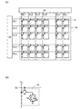
次いで、図5(B)に示す画素31の、レイアウトの一例を図7に示す。なお、図7では、画素31のレイアウトを明確にするために、ゲート絶縁膜などの各種の絶縁膜や酸化物膜を省略している。また、図7に示す素子基板を用いて形成された液晶表示装置の断面図を、図8に示す。図8に示す液晶表示装置のうち、第1基板10を含む素子基板は、図7の破線A1−A2における断面図に相当する。
次いで、図7に示した素子基板の作製方法について、一例を挙げて説明する。なお、酸化物半導体膜にチャネル形成領域を有するトランジスタ35を例に挙げて素子基板の作製方法について説明するが、トランジスタ35は、非晶質、微結晶、多結晶または単結晶である、シリコン又はゲルマニウムなどの半導体膜を活性層に用いることもできる。
なお、電子供与体(ドナー)となる水分または水素などの不純物が低減され、なおかつ酸素欠損が低減されることにより高純度化された酸化物半導体(purified Oxide Semiconductor)は、i型(真性半導体)又はi型に限りなく近い。そのため、高純度化された酸化物半導体膜にチャネル形成領域を有するトランジスタは、オフ電流が著しく小さく、信頼性が高い。
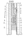
本発明の一態様に係る液晶表示装置の外観について、図12を用いて説明する。図12は、第1基板4001と第2基板4006とを封止材4005によって接着させた液晶表示装置の上面図である。また、図13は、図12の破線B1−B2における断面図に相当する。なお、図12では、FFSモードの液晶表示装置を例示している。
本発明の一態様に係る液晶表示装置は、表示機器、パーソナルコンピュータ、記録媒体を備えた画像再生装置(代表的にはDVD:Digital Versatile Disc等の記録媒体を再生し、その画像を表示しうるディスプレイを有する装置)に用いることができる。その他に、本発明の一態様に係る液晶表示装置を用いることができる電子機器として、携帯電話、携帯型を含むゲーム機、携帯情報端末、電子書籍、ビデオカメラ、デジタルスチルカメラなどのカメラ、ゴーグル型ディスプレイ(ヘッドマウントディスプレイ)、ナビゲーションシステム、音響再生装置(カーオーディオ、デジタルオーディオプレイヤー等)、複写機、ファクシミリ、プリンター、プリンター複合機、現金自動預け入れ払い機(ATM)、自動販売機などが挙げられる。これら電子機器の具体例を図14に示す。
11 素子層
12 電極
13 絶縁膜
14 電極
15 トランジスタ
16 画素
20 第2基板
21 電極
21a 導電膜
21b 導電膜
21c 導電膜
21d 導電膜
22 絶縁膜
23 電極
24 樹脂膜
25 導電膜
26 容量
27 導電体
28 液晶層
30 画素部
31 画素
32 駆動回路
33 駆動回路
34 液晶素子
35 トランジスタ
36 容量素子
38 パネル
40 液晶表示装置
41 コントローラ
43 CPU
44 画像処理回路
45 画像メモリ
46 画像データ
51 導電膜
53 絶縁膜
54 半導体膜
55 導電膜
56 導電膜
57 酸化物膜
58 絶縁膜
59 絶縁膜
60 有機樹脂膜
61 導電膜
62 開口部
63 絶縁膜
64 導電膜
65 配向膜
66 絶縁膜
67 遮蔽膜
68 着色層
69 配向膜
4001 第1基板
4002 画素部
4003 駆動回路
4004 駆動回路
4005 封止材
4006 第2基板
4010 トランジスタ
4018 FPC
4020 絶縁膜
4021 画素電極
4022 絶縁膜
4023 液晶素子
4024 共通電極
4028 液晶層
4030 配線
4050 導電膜
4051 導電膜
4052 導電膜
4053 導電膜
4054 ゲート絶縁膜
4056 電極
4057 電極
4058 絶縁膜
4059 樹脂膜
4060 導電膜
4061 導電性粒子
4062 樹脂膜
5001 筐体
5002 筐体
5003 表示部
5004 表示部
5005 マイクロホン
5006 スピーカー
5007 操作キー
5008 スタイラス
5201 筐体
5202 表示部
5203 支持台
5401 筐体
5402 表示部
5403 キーボード
5404 ポインティングデバイス
5601 筐体
5602 筐体
5603 表示部
5604 表示部
5605 接続部
5606 操作キー
5801 筐体
5802 筐体
5803 表示部
5804 操作キー
5805 レンズ
5806 接続部
5901 筐体
5902 表示部
5903 カメラ
5904 スピーカー
5905 ボタン
5906 外部接続部
5907 マイク
Claims (4)
- 第1の基板と、
前記第1の基板上の素子層と、
前記素子層上の液晶素子と、
前記液晶素子上の導電膜と、
前記導電膜上の樹脂膜と、
前記樹脂膜上の第1の電極と
前記第1の電極と第1の絶縁膜を介して重なる領域を有する第2の電極と、
前記第2の電極上の第2の基板と、を有し、
前記素子層は、酸化物半導体をチャネル形成領域に含むトランジスタを有し、
前記トランジスタは、前記液晶素子への画像信号の供給を制御する機能を有し、
前記液晶素子は、画素電極と、共通電極と、前記画素電極及び前記共通電極から電界が加えられる液晶層と、を有し、
前記画素電極は、第2の絶縁膜を介して前記共通電極と重なる領域を有し、
前記画素電極は、前記共通電極上に位置し、
前記画素電極は、前記共通電極の開口部を介して前記トランジスタのソース又はドレインの一方と電気的に接続されており、
前記共通電極の開口部は、前記トランジスタのチャネル形成領域と重なっており、
前記トランジスタのチャネル形成領域は、前記共通電極と重なっておらず、
前記第1の電極は、前記第2の電極と交差しており、
前記導電膜には第1の電位が供給される液晶表示装置であって、
前記液晶表示装置は、前記第1の電極と前記第2の電極とを用いて位置情報の取得を行う機能を有する液晶表示装置。 - 第1の基板と、
前記第1の基板上の素子層と、
前記素子層上の液晶素子と、
前記液晶素子上の導電膜と、
前記導電膜上の樹脂膜と、
前記樹脂膜上の第1の電極と
前記第1の電極と第1の絶縁膜を介して重なる領域を有する第2の電極と、
前記第2の電極上の第2の基板と、を有し、
前記素子層は、酸化物半導体をチャネル形成領域に含むトランジスタを有し、
前記トランジスタは、前記液晶素子への画像信号の供給を制御する機能を有し、
前記液晶素子は、画素電極と、共通電極と、前記画素電極及び前記共通電極から電界が加えられる液晶層と、を有し、
前記画素電極は、第2の絶縁膜を介して前記共通電極と重なる領域を有し、
前記画素電極は、前記共通電極上に位置し、
前記画素電極は、前記共通電極の開口部を介して前記トランジスタのソース又はドレインの一方と電気的に接続されており、
前記共通電極の開口部は、前記トランジスタのチャネル形成領域と重なっており、
前記トランジスタのチャネル形成領域は、前記共通電極と重なっておらず、
前記第1の電極は、前記第2の電極と交差しており、
前記導電膜は、前記共通電極と電気的に接続される液晶表示装置であって、
前記液晶表示装置は、前記第1の電極と前記第2の電極とを用いて位置情報の取得を行う機能を有する液晶表示装置。 - 第1の基板と、
前記第1の基板上の素子層と、
前記素子層上の液晶素子と、
前記液晶素子上の導電膜と、
前記導電膜上の樹脂膜と、
前記樹脂膜上の第1の電極と
前記第1の電極と第1の絶縁膜を介して重なる領域を有する第2の電極と、
前記第2の電極上の第2の基板と、を有し、
前記素子層は、酸化物半導体をチャネル形成領域に含むトランジスタを有し、
前記トランジスタは、前記液晶素子への画像信号の書き込みを制御する機能を有し、
前記液晶素子は、画素電極と、共通電極と、前記画素電極及び前記共通電極から電界が加えられる液晶層と、を有し、
前記画素電極は、第2の絶縁膜を介して前記共通電極と重なる領域を有し、
前記画素電極は、前記共通電極上に位置し、
前記画素電極は、前記共通電極の開口部を介して前記トランジスタのソース又はドレインの一方と電気的に接続されており、
前記共通電極の開口部は、前記トランジスタのチャネル形成領域と重なっており、
前記トランジスタのチャネル形成領域は、前記共通電極と重なっておらず、
前記第1の電極は、前記第2の電極と交差しており、
前記導電膜には第1の電位が供給される液晶表示装置であって、
第1の期間と、第2の期間と、を有し、
前記第1の期間では静止画の表示を行い、
前記第2の期間では動画の表示を行い、
前記第1の期間における一定期間内の前記液晶素子への前記画像信号の書き込みの回数は、前記第2の期間における一定期間内の前記液晶素子への前記画像信号の書き込みの回数よりも少なく、
前記液晶表示装置は、前記第1の電極と前記第2の電極とを用いて位置情報の取得を行う機能を有する液晶表示装置。 - 第1の基板と、
前記第1の基板上の素子層と、
前記素子層上の液晶素子と、
前記液晶素子上の導電膜と、
前記導電膜上の樹脂膜と、
前記樹脂膜上の第1の電極と
前記第1の電極と第1の絶縁膜を介して重なる領域を有する第2の電極と、
前記第2の電極上の第2の基板と、を有し、
前記素子層は、酸化物半導体をチャネル形成領域に含むトランジスタを有し、
前記トランジスタは、前記液晶素子への画像信号の供給を制御する機能を有し、
前記液晶素子は、画素電極と、共通電極と、前記画素電極及び前記共通電極から電界が加えられる液晶層と、を有し、
前記画素電極は、第2の絶縁膜を介して前記共通電極と重なる領域を有し、
前記画素電極は、前記共通電極上に位置し、
前記画素電極は、前記共通電極の開口部を介して前記トランジスタのソース又はドレインの一方と電気的に接続されており、
前記共通電極の開口部は、前記トランジスタのチャネル形成領域と重なっており、
前記トランジスタのチャネル形成領域は、前記共通電極と重なっておらず、
前記第1の電極は、前記第2の電極と交差しており、
前記導電膜は、前記共通電極と電気的に接続される液晶表示装置であって、
第1の期間と、第2の期間と、を有し、
前記第1の期間では静止画の表示を行い、
前記第2の期間では動画の表示を行い、
前記第1の期間における一定期間内の前記液晶素子への前記画像信号の書き込みの回数は、前記第2の期間における一定期間内の前記液晶素子への前記画像信号の書き込みの回数よりも少なく、
前記液晶表示装置は、前記第1の電極と前記第2の電極とを用いて位置情報の取得を行う機能を有する液晶表示装置。
Priority Applications (1)
| Application Number | Priority Date | Filing Date | Title |
|---|---|---|---|
| JP2014054832A JP6503157B2 (ja) | 2013-03-22 | 2014-03-18 | 液晶表示装置 |
Applications Claiming Priority (3)
| Application Number | Priority Date | Filing Date | Title |
|---|---|---|---|
| JP2013059637 | 2013-03-22 | ||
| JP2013059637 | 2013-03-22 | ||
| JP2014054832A JP6503157B2 (ja) | 2013-03-22 | 2014-03-18 | 液晶表示装置 |
Related Child Applications (1)
| Application Number | Title | Priority Date | Filing Date |
|---|---|---|---|
| JP2019056503A Division JP6714744B2 (ja) | 2013-03-22 | 2019-03-25 | 液晶表示装置 |
Publications (3)
| Publication Number | Publication Date |
|---|---|
| JP2014209204A JP2014209204A (ja) | 2014-11-06 |
| JP2014209204A5 JP2014209204A5 (ja) | 2017-04-13 |
| JP6503157B2 true JP6503157B2 (ja) | 2019-04-17 |
Family
ID=51568902
Family Applications (5)
| Application Number | Title | Priority Date | Filing Date |
|---|---|---|---|
| JP2014054832A Active JP6503157B2 (ja) | 2013-03-22 | 2014-03-18 | 液晶表示装置 |
| JP2019056503A Active JP6714744B2 (ja) | 2013-03-22 | 2019-03-25 | 液晶表示装置 |
| JP2020098205A Active JP7021294B2 (ja) | 2013-03-22 | 2020-06-05 | 液晶表示装置 |
| JP2022015453A Withdrawn JP2022063283A (ja) | 2013-03-22 | 2022-02-03 | 液晶表示装置 |
| JP2023107906A Pending JP2023115339A (ja) | 2013-03-22 | 2023-06-30 | 液晶表示装置 |
Family Applications After (4)
| Application Number | Title | Priority Date | Filing Date |
|---|---|---|---|
| JP2019056503A Active JP6714744B2 (ja) | 2013-03-22 | 2019-03-25 | 液晶表示装置 |
| JP2020098205A Active JP7021294B2 (ja) | 2013-03-22 | 2020-06-05 | 液晶表示装置 |
| JP2022015453A Withdrawn JP2022063283A (ja) | 2013-03-22 | 2022-02-03 | 液晶表示装置 |
| JP2023107906A Pending JP2023115339A (ja) | 2013-03-22 | 2023-06-30 | 液晶表示装置 |
Country Status (4)
| Country | Link |
|---|---|
| US (3) | US9581849B2 (ja) |
| JP (5) | JP6503157B2 (ja) |
| KR (4) | KR102141459B1 (ja) |
| TW (4) | TW202321793A (ja) |
Cited By (1)
| Publication number | Priority date | Publication date | Assignee | Title |
|---|---|---|---|---|
| JP2019117405A (ja) * | 2013-03-22 | 2019-07-18 | 株式会社半導体エネルギー研究所 | 液晶表示装置 |
Families Citing this family (35)
| Publication number | Priority date | Publication date | Assignee | Title |
|---|---|---|---|---|
| US8562770B2 (en) | 2008-05-21 | 2013-10-22 | Manufacturing Resources International, Inc. | Frame seal methods for LCD |
| US9573346B2 (en) | 2008-05-21 | 2017-02-21 | Manufacturing Resources International, Inc. | Photoinitiated optical adhesive and method for using same |
| US9881528B2 (en) | 2011-10-13 | 2018-01-30 | Manufacturing Resources International, Inc. | Transparent liquid crystal display on display case |
| JP6518133B2 (ja) | 2014-05-30 | 2019-05-22 | 株式会社半導体エネルギー研究所 | 入力装置 |
| US9526352B2 (en) * | 2014-06-16 | 2016-12-27 | Manufacturing Resources International, Inc. | Wireless video transmission system for liquid crystal display |
| US9633366B2 (en) | 2014-06-16 | 2017-04-25 | Manufacturing Resources International, Inc. | System for tracking and analyzing display case usage |
| US9500896B2 (en) | 2014-06-16 | 2016-11-22 | Manufacturing Resources International, Inc. | Cooling system for liquid crystal display |
| US9535293B2 (en) | 2014-06-16 | 2017-01-03 | Manufacturing Resources International, Inc. | Sealed transparent liquid crystal display assembly |
| US9500801B2 (en) * | 2014-06-16 | 2016-11-22 | Manufacturing Resources International, Inc. | LED assembly for transparent liquid crystal display |
| US10649273B2 (en) | 2014-10-08 | 2020-05-12 | Manufacturing Resources International, Inc. | LED assembly for transparent liquid crystal display and static graphic |
| US9832847B2 (en) | 2014-10-09 | 2017-11-28 | Manufacturing Resources International, Inc. | System for decreasing energy usage of a transparent LCD display case |
| US10182665B2 (en) | 2014-10-15 | 2019-01-22 | Manufacturing Resources International, Inc. | System and method for preventing damage to products |
| KR102500994B1 (ko) | 2014-10-17 | 2023-02-16 | 가부시키가이샤 한도오따이 에네루기 켄큐쇼 | 터치 패널 |
| US9933872B2 (en) | 2014-12-01 | 2018-04-03 | Semiconductor Energy Laboratory Co., Ltd. | Touch panel |
| JP6698321B2 (ja) | 2014-12-02 | 2020-05-27 | 株式会社半導体エネルギー研究所 | 表示装置 |
| JP6765199B2 (ja) | 2015-03-17 | 2020-10-07 | 株式会社半導体エネルギー研究所 | タッチパネル |
| WO2016147074A1 (en) * | 2015-03-17 | 2016-09-22 | Semiconductor Energy Laboratory Co., Ltd. | Touch panel |
| KR20160114510A (ko) * | 2015-03-24 | 2016-10-05 | 가부시키가이샤 한도오따이 에네루기 켄큐쇼 | 터치 패널 |
| US10372274B2 (en) | 2015-04-13 | 2019-08-06 | Semiconductor Energy Laboratory Co., Ltd. | Semiconductor device and touch panel |
| US10671204B2 (en) | 2015-05-04 | 2020-06-02 | Semiconductor Energy Laboratory Co., Ltd. | Touch panel and data processor |
| US10684500B2 (en) | 2015-05-27 | 2020-06-16 | Semiconductor Energy Laboratory Co., Ltd. | Touch panel |
| WO2016189426A1 (ja) | 2015-05-28 | 2016-12-01 | 株式会社半導体エネルギー研究所 | タッチパネル |
| CN106249493B (zh) * | 2015-06-05 | 2019-10-11 | 群创光电股份有限公司 | 显示装置 |
| KR102619052B1 (ko) | 2015-06-15 | 2023-12-29 | 가부시키가이샤 한도오따이 에네루기 켄큐쇼 | 표시 장치 |
| US10325131B2 (en) * | 2015-06-30 | 2019-06-18 | Synaptics Incorporated | Active matrix capacitive fingerprint sensor for display integration based on charge sensing by a 2-TFT pixel architecture |
| US11043543B2 (en) | 2015-07-07 | 2021-06-22 | Semiconductor Energy Laboratory Co., Ltd. | Touch sensor and touch panel |
| CN105116589A (zh) * | 2015-09-25 | 2015-12-02 | 深圳市华星光电技术有限公司 | 阵列基板、透光钝化膜及液晶显示面板的制造方法 |
| JP2019513251A (ja) | 2016-03-02 | 2019-05-23 | マニュファクチャリング・リソーシズ・インターナショナル・インコーポレーテッド | 透明ディスプレイを備える自動販売機 |
| TWI769995B (zh) | 2016-06-24 | 2022-07-11 | 日商半導體能源研究所股份有限公司 | 顯示裝置、電子裝置 |
| KR20190026850A (ko) | 2016-07-08 | 2019-03-13 | 매뉴팩처링 리소시스 인터내셔널 인코포레이티드 | 통합형 전자 디스플레이를 갖는 미러 |
| KR102365490B1 (ko) | 2016-07-13 | 2022-02-18 | 가부시키가이샤 한도오따이 에네루기 켄큐쇼 | 입출력 패널, 입출력 장치, 반도체 장치 |
| KR102517810B1 (ko) | 2016-08-17 | 2023-04-05 | 엘지디스플레이 주식회사 | 표시장치 |
| US20180145096A1 (en) * | 2016-11-23 | 2018-05-24 | Semiconductor Energy Laboratory Co., Ltd. | Display device and electronic device |
| TWI622911B (zh) * | 2017-02-14 | 2018-05-01 | 宏碁股份有限公司 | 觸控裝置 |
| CN114384715B (zh) * | 2021-12-29 | 2023-06-06 | 武汉天马微电子有限公司 | 显示面板和显示装置 |
Family Cites Families (76)
| Publication number | Priority date | Publication date | Assignee | Title |
|---|---|---|---|---|
| JPS5837549U (ja) | 1981-09-08 | 1983-03-11 | 日本ゼオン株式会社 | 粘着テ−プ等の保持力測定装置 |
| JP3963974B2 (ja) | 1995-12-20 | 2007-08-22 | 株式会社半導体エネルギー研究所 | 液晶電気光学装置 |
| US6346932B1 (en) * | 1996-03-14 | 2002-02-12 | Seiko Epson Corporation | Liquid crystal device and electronic equipment |
| US6184946B1 (en) * | 1996-11-27 | 2001-02-06 | Hitachi, Ltd. | Active matrix liquid crystal display |
| JP4117148B2 (ja) | 2002-05-24 | 2008-07-16 | 日本電気株式会社 | 半透過型液晶表示装置 |
| JP2005292709A (ja) | 2004-04-05 | 2005-10-20 | Toshiba Matsushita Display Technology Co Ltd | 液晶表示素子 |
| KR20060115427A (ko) | 2005-05-04 | 2006-11-09 | 삼성전자주식회사 | 액정 표시 장치 |
| EP1958019B1 (en) | 2005-12-05 | 2017-04-12 | Semiconductor Energy Laboratory Co., Ltd. | Liquid crystal display device |
| JP2007212498A (ja) * | 2006-02-07 | 2007-08-23 | Epson Imaging Devices Corp | 液晶表示装置、液晶表示装置の製造方法及び電子機器 |
| WO2007102238A1 (ja) | 2006-03-08 | 2007-09-13 | Sharp Kabushiki Kaisha | 表示装置 |
| JP4466596B2 (ja) | 2006-03-29 | 2010-05-26 | カシオ計算機株式会社 | 配向転移方法 |
| KR20090028627A (ko) | 2006-06-09 | 2009-03-18 | 애플 인크. | 터치 스크린 액정 디스플레이 |
| CN101467119B (zh) | 2006-06-09 | 2013-02-13 | 苹果公司 | 触摸屏液晶显示器 |
| KR101295943B1 (ko) * | 2006-06-09 | 2013-08-13 | 애플 인크. | 터치 스크린 액정 디스플레이 |
| US8243027B2 (en) | 2006-06-09 | 2012-08-14 | Apple Inc. | Touch screen liquid crystal display |
| CN104965621B (zh) | 2006-06-09 | 2018-06-12 | 苹果公司 | 触摸屏液晶显示器及其操作方法 |
| KR101264693B1 (ko) | 2006-06-30 | 2013-05-16 | 엘지디스플레이 주식회사 | 횡전계방식 액정표시장치 및 그 구동방법 |
| US20080167526A1 (en) | 2007-01-08 | 2008-07-10 | Crank Justin M | Non-Occlusive, Laterally-Constrained Injection Device |
| KR100851207B1 (ko) | 2007-01-16 | 2008-08-07 | 삼성에스디아이 주식회사 | 2차원 및 3차원 영상 선택 가능 디스플레이 장치 |
| JP5008026B2 (ja) * | 2007-01-30 | 2012-08-22 | ソニーモバイルディスプレイ株式会社 | 入力機能付表示装置 |
| JP5051690B2 (ja) | 2007-01-30 | 2012-10-17 | 株式会社ジャパンディスプレイウェスト | 入力機能付表示装置 |
| KR20080073573A (ko) * | 2007-02-06 | 2008-08-11 | 엘지디스플레이 주식회사 | 액정패널과 이의 제조방법 |
| JP2008299312A (ja) * | 2007-05-01 | 2008-12-11 | Epson Imaging Devices Corp | 液晶表示装置および電子機器 |
| KR101304411B1 (ko) | 2007-05-03 | 2013-09-05 | 삼성디스플레이 주식회사 | 표시 장치 |
| CN100472290C (zh) | 2007-08-30 | 2009-03-25 | 深圳和而泰智能控制股份有限公司 | 电容式触摸屏及制作方法 |
| KR20090023117A (ko) | 2007-08-31 | 2009-03-04 | 세이코 엡슨 가부시키가이샤 | 액정 장치, 액정 장치의 구동 방법, 액정 장치 구동용 집적회로 장치 및 전자 기기 |
| KR101374108B1 (ko) | 2007-10-30 | 2014-03-13 | 엘지디스플레이 주식회사 | 액정 표시 패널과 그 제조 방법 |
| TW200921483A (en) * | 2007-11-09 | 2009-05-16 | Tpk Touch Solutions Inc | Touch-control display panel with an electric-field shielding layer |
| US20090190077A1 (en) | 2007-12-21 | 2009-07-30 | Chung Yuan Christian University | Bistable SmA liquid-crystal display |
| JP4678031B2 (ja) * | 2008-01-11 | 2011-04-27 | ソニー株式会社 | 液晶装置および電子機器 |
| JP4816668B2 (ja) | 2008-03-28 | 2011-11-16 | ソニー株式会社 | タッチセンサ付き表示装置 |
| TW200949649A (en) * | 2008-05-16 | 2009-12-01 | Emerging Display Tech Corp | A LCD panel with built-in capacitive-type touch-control panel |
| JP5483143B2 (ja) * | 2008-09-22 | 2014-05-07 | 大日本印刷株式会社 | カラーフィルタ、表示装置、および、カラーフィルタの製造方法 |
| US20100091231A1 (en) * | 2008-10-14 | 2010-04-15 | Seiko Epson Corporation | Liquid crystal display device and electronic apparatus |
| JP5512138B2 (ja) * | 2009-01-30 | 2014-06-04 | 株式会社ジャパンディスプレイ | 液晶表示装置 |
| JP2010191287A (ja) * | 2009-02-19 | 2010-09-02 | Hitachi Displays Ltd | 表示装置 |
| TWI403946B (zh) * | 2009-06-15 | 2013-08-01 | Au Optronics Corp | 顯示裝置及其應用方法 |
| TWI497157B (zh) * | 2009-06-19 | 2015-08-21 | Tpk Touch Solutions Inc | 具觸控功能的平面轉換式液晶顯示器 |
| JP5297927B2 (ja) * | 2009-07-22 | 2013-09-25 | 株式会社ジャパンディスプレイウェスト | 液晶表示パネル |
| CN101963713A (zh) * | 2009-07-24 | 2011-02-02 | 宸鸿光电科技股份有限公司 | 具有触控功能的平面转换式液晶显示器 |
| US20120223308A1 (en) * | 2009-10-16 | 2012-09-06 | Sharp Kabushiki Kaisha | Thin-film transistor, process for production of same, and display device equipped with same |
| TWI390291B (zh) | 2009-12-15 | 2013-03-21 | Au Optronics Corp | 液晶顯示裝置 |
| JP5377279B2 (ja) * | 2009-12-28 | 2013-12-25 | 株式会社ジャパンディスプレイ | 静電容量型入力装置および入力機能付き電気光学装置 |
| TW201124766A (en) * | 2010-01-08 | 2011-07-16 | Wintek Corp | Display device with touch panel |
| US20120242923A1 (en) * | 2010-02-25 | 2012-09-27 | Sharp Kabushiki Kaisha | Thin film transistor substrate, method for manufacturing the same, and display device |
| KR101305378B1 (ko) | 2010-03-19 | 2013-09-06 | 엘지디스플레이 주식회사 | 터치인식 횡전계형 액정표시장치 및 이의 제조 방법 |
| JP5013554B2 (ja) * | 2010-03-31 | 2012-08-29 | 株式会社ジャパンディスプレイセントラル | 液晶表示装置 |
| KR20220005640A (ko) * | 2010-04-28 | 2022-01-13 | 가부시키가이샤 한도오따이 에네루기 켄큐쇼 | 표시 장치 |
| JP5458443B2 (ja) | 2010-09-14 | 2014-04-02 | 株式会社ジャパンディスプレイ | タッチ検出機能付き表示装置、および電子機器 |
| KR101729682B1 (ko) | 2010-11-04 | 2017-04-25 | 삼성디스플레이 주식회사 | 광학 유닛 및 이를 포함하는 표시 장치 |
| JP5134676B2 (ja) * | 2010-11-24 | 2013-01-30 | 株式会社ジャパンディスプレイイースト | 液晶表示装置およびその製造方法 |
| JP5090553B2 (ja) * | 2011-03-30 | 2012-12-05 | アルプス電気株式会社 | 表面パネルおよびその製造方法 |
| JP2012220670A (ja) * | 2011-04-07 | 2012-11-12 | Toppan Printing Co Ltd | タッチパネル電極付きカラーフィルタとその製造方法 |
| US8988624B2 (en) * | 2011-06-23 | 2015-03-24 | Apple Inc. | Display pixel having oxide thin-film transistor (TFT) with reduced loading |
| KR20130005660A (ko) * | 2011-07-07 | 2013-01-16 | 삼성전자주식회사 | 터치스크린패널 액정디스플레이장치 |
| US9405330B2 (en) | 2011-07-29 | 2016-08-02 | Sharp Kabushiki Kaisha | Touch panel substrate and display panel |
| US9470941B2 (en) * | 2011-08-19 | 2016-10-18 | Apple Inc. | In-cell or on-cell touch sensor with color filter on array |
| JP5647955B2 (ja) * | 2011-08-24 | 2015-01-07 | 株式会社ジャパンディスプレイ | 液晶表示装置 |
| JP2013080185A (ja) * | 2011-10-05 | 2013-05-02 | Japan Display East Co Ltd | 液晶表示装置 |
| US9417746B2 (en) * | 2012-02-09 | 2016-08-16 | Sharp Kabushiki Kaisha | Touch-panel substrate |
| TWM442547U (en) * | 2012-05-02 | 2012-12-01 | Apex Material Technology Corp | Electrode layer for use in touch panel |
| KR20130127848A (ko) * | 2012-05-15 | 2013-11-25 | 삼성전기주식회사 | 터치센서 및 그 제조방법 |
| JP2015148637A (ja) | 2012-05-23 | 2015-08-20 | シャープ株式会社 | 液晶表示装置 |
| TWM440479U (en) * | 2012-06-06 | 2012-11-01 | J Touch Corp | Capacitive touch sensor |
| JP2015163908A (ja) | 2012-06-21 | 2015-09-10 | シャープ株式会社 | 液晶表示装置 |
| KR101975930B1 (ko) | 2012-07-04 | 2019-05-07 | 엘지디스플레이 주식회사 | 듀얼모드 액정표시장치의 구동방법 |
| JP2015179100A (ja) | 2012-07-23 | 2015-10-08 | シャープ株式会社 | 液晶表示装置 |
| CN102841716B (zh) * | 2012-08-21 | 2015-08-05 | 北京京东方光电科技有限公司 | 一种电容式内嵌触摸屏及显示装置 |
| CN102841466B (zh) * | 2012-09-20 | 2015-08-26 | 昆山龙腾光电有限公司 | 液晶显示装置 |
| US20140152922A1 (en) | 2012-12-05 | 2014-06-05 | Samsung Display Co., Ltd. | Liquid crystal display and method of manufacturing the same |
| CN102998840A (zh) | 2012-12-12 | 2013-03-27 | 京东方科技集团股份有限公司 | 显示面板以及具有该显示面板的显示装置 |
| US9552785B2 (en) | 2012-12-19 | 2017-01-24 | Sharp Kabushiki Kaisha | Liquid crystal display device |
| JP2014186724A (ja) * | 2013-02-22 | 2014-10-02 | Semiconductor Energy Lab Co Ltd | 表示装置 |
| KR102141459B1 (ko) | 2013-03-22 | 2020-08-05 | 가부시키가이샤 한도오따이 에네루기 켄큐쇼 | 액정 표시 장치 |
| TWI545373B (zh) | 2013-09-25 | 2016-08-11 | 群創光電股份有限公司 | 自發光顯示元件 |
| EP2983040B1 (en) | 2014-07-25 | 2019-05-22 | LG Display Co., Ltd. | Transparent display based on a guest-host cholesteric liquid crystal device |
-
2014
- 2014-03-05 KR KR1020140026158A patent/KR102141459B1/ko active IP Right Grant
- 2014-03-06 TW TW111136050A patent/TW202321793A/zh unknown
- 2014-03-06 TW TW110123417A patent/TWI779688B/zh active
- 2014-03-06 TW TW103107693A patent/TWI621899B/zh not_active IP Right Cessation
- 2014-03-06 TW TW107103664A patent/TWI732991B/zh not_active IP Right Cessation
- 2014-03-18 US US14/217,578 patent/US9581849B2/en active Active
- 2014-03-18 JP JP2014054832A patent/JP6503157B2/ja active Active
-
2017
- 2017-02-15 US US15/433,539 patent/US10317717B2/en active Active
-
2018
- 2018-02-07 US US15/890,404 patent/US10901255B2/en active Active
-
2019
- 2019-03-25 JP JP2019056503A patent/JP6714744B2/ja active Active
-
2020
- 2020-06-05 JP JP2020098205A patent/JP7021294B2/ja active Active
- 2020-07-29 KR KR1020200094369A patent/KR102354348B1/ko active IP Right Grant
-
2022
- 2022-01-10 KR KR1020220003271A patent/KR102414062B1/ko active IP Right Grant
- 2022-02-03 JP JP2022015453A patent/JP2022063283A/ja not_active Withdrawn
- 2022-06-22 KR KR1020220076321A patent/KR102479009B1/ko active IP Right Grant
-
2023
- 2023-06-30 JP JP2023107906A patent/JP2023115339A/ja active Pending
Cited By (2)
| Publication number | Priority date | Publication date | Assignee | Title |
|---|---|---|---|---|
| JP2019117405A (ja) * | 2013-03-22 | 2019-07-18 | 株式会社半導体エネルギー研究所 | 液晶表示装置 |
| US10901255B2 (en) | 2013-03-22 | 2021-01-26 | Semiconductor Energy Laboratory Co., Ltd. | Liquid crystal display device |
Also Published As
| Publication number | Publication date |
|---|---|
| KR20220008375A (ko) | 2022-01-20 |
| TW201441743A (zh) | 2014-11-01 |
| TWI621899B (zh) | 2018-04-21 |
| TWI779688B (zh) | 2022-10-01 |
| JP2019117405A (ja) | 2019-07-18 |
| JP6714744B2 (ja) | 2020-06-24 |
| KR102354348B1 (ko) | 2022-01-20 |
| JP2014209204A (ja) | 2014-11-06 |
| US10317717B2 (en) | 2019-06-11 |
| US9581849B2 (en) | 2017-02-28 |
| US10901255B2 (en) | 2021-01-26 |
| TW202138890A (zh) | 2021-10-16 |
| KR20140115972A (ko) | 2014-10-01 |
| KR102479009B1 (ko) | 2022-12-16 |
| KR102141459B1 (ko) | 2020-08-05 |
| JP2022063283A (ja) | 2022-04-21 |
| JP2020149069A (ja) | 2020-09-17 |
| KR102414062B1 (ko) | 2022-06-27 |
| TW202321793A (zh) | 2023-06-01 |
| US20170160576A1 (en) | 2017-06-08 |
| TW201827904A (zh) | 2018-08-01 |
| JP2023115339A (ja) | 2023-08-18 |
| JP7021294B2 (ja) | 2022-02-16 |
| KR20220092835A (ko) | 2022-07-04 |
| TWI732991B (zh) | 2021-07-11 |
| KR20200093506A (ko) | 2020-08-05 |
| US20140285732A1 (en) | 2014-09-25 |
| US20180164625A1 (en) | 2018-06-14 |
Similar Documents
| Publication | Publication Date | Title |
|---|---|---|
| JP7021294B2 (ja) | 液晶表示装置 | |
| JP7072601B2 (ja) | 液晶表示装置 | |
| KR102412707B1 (ko) | 표시 장치 | |
| KR102156943B1 (ko) | 액정 표시 장치, 터치 패널 | |
| JP6351947B2 (ja) | 液晶表示装置の作製方法 | |
| US9594281B2 (en) | Liquid crystal display device |
Legal Events
| Date | Code | Title | Description |
|---|---|---|---|
| A521 | Request for written amendment filed |
Free format text: JAPANESE INTERMEDIATE CODE: A523 Effective date: 20170313 |
|
| A621 | Written request for application examination |
Free format text: JAPANESE INTERMEDIATE CODE: A621 Effective date: 20170313 |
|
| A977 | Report on retrieval |
Free format text: JAPANESE INTERMEDIATE CODE: A971007 Effective date: 20171219 |
|
| A131 | Notification of reasons for refusal |
Free format text: JAPANESE INTERMEDIATE CODE: A131 Effective date: 20180206 |
|
| A521 | Request for written amendment filed |
Free format text: JAPANESE INTERMEDIATE CODE: A523 Effective date: 20180402 |
|
| A131 | Notification of reasons for refusal |
Free format text: JAPANESE INTERMEDIATE CODE: A131 Effective date: 20180925 |
|
| A521 | Request for written amendment filed |
Free format text: JAPANESE INTERMEDIATE CODE: A523 Effective date: 20181022 |
|
| TRDD | Decision of grant or rejection written | ||
| A01 | Written decision to grant a patent or to grant a registration (utility model) |
Free format text: JAPANESE INTERMEDIATE CODE: A01 Effective date: 20190226 |
|
| A61 | First payment of annual fees (during grant procedure) |
Free format text: JAPANESE INTERMEDIATE CODE: A61 Effective date: 20190325 |
|
| R150 | Certificate of patent or registration of utility model |
Ref document number: 6503157 Country of ref document: JP Free format text: JAPANESE INTERMEDIATE CODE: R150 |
|
| R250 | Receipt of annual fees |
Free format text: JAPANESE INTERMEDIATE CODE: R250 |
|
| R250 | Receipt of annual fees |
Free format text: JAPANESE INTERMEDIATE CODE: R250 |
|
| R250 | Receipt of annual fees |
Free format text: JAPANESE INTERMEDIATE CODE: R250 |