JP6443457B2 - Vapor deposition mask and method of manufacturing vapor deposition mask - Google Patents

Vapor deposition mask and method of manufacturing vapor deposition mask Download PDF

Info

Publication number
JP6443457B2
JP6443457B2 JP2016564655A JP2016564655A JP6443457B2 JP 6443457 B2 JP6443457 B2 JP 6443457B2 JP 2016564655 A JP2016564655 A JP 2016564655A JP 2016564655 A JP2016564655 A JP 2016564655A JP 6443457 B2 JP6443457 B2 JP 6443457B2
Authority
JP
Japan
Prior art keywords
vapor deposition
metal layer
deposition mask
mask
substrate
Prior art date
Legal status (The legal status is an assumption and is not a legal conclusion. Google has not performed a legal analysis and makes no representation as to the accuracy of the status listed.)
Active
Application number
JP2016564655A
Other languages
Japanese (ja)
Other versions
JPWO2017057621A1 (en
Inventor
永 知加雄 池
永 知加雄 池
崎 洋 島
崎 洋 島
謙太朗 関
謙太朗 関
庄 宏 樹 古
庄 宏 樹 古
田 千 秋 初
田 千 秋 初
Current Assignee (The listed assignees may be inaccurate. Google has not performed a legal analysis and makes no representation or warranty as to the accuracy of the list.)
Dai Nippon Printing Co Ltd
Original Assignee
Dai Nippon Printing Co Ltd
Priority date (The priority date is an assumption and is not a legal conclusion. Google has not performed a legal analysis and makes no representation as to the accuracy of the date listed.)
Filing date
Publication date
Application filed by Dai Nippon Printing Co Ltd filed Critical Dai Nippon Printing Co Ltd
Publication of JPWO2017057621A1 publication Critical patent/JPWO2017057621A1/en
Priority to JP2018139772A priority Critical patent/JP6939732B2/en
Application granted granted Critical
Publication of JP6443457B2 publication Critical patent/JP6443457B2/en
Active legal-status Critical Current
Anticipated expiration legal-status Critical

Links

Images

Classifications

    • CCHEMISTRY; METALLURGY
    • C23COATING METALLIC MATERIAL; COATING MATERIAL WITH METALLIC MATERIAL; CHEMICAL SURFACE TREATMENT; DIFFUSION TREATMENT OF METALLIC MATERIAL; COATING BY VACUUM EVAPORATION, BY SPUTTERING, BY ION IMPLANTATION OR BY CHEMICAL VAPOUR DEPOSITION, IN GENERAL; INHIBITING CORROSION OF METALLIC MATERIAL OR INCRUSTATION IN GENERAL
    • C23CCOATING METALLIC MATERIAL; COATING MATERIAL WITH METALLIC MATERIAL; SURFACE TREATMENT OF METALLIC MATERIAL BY DIFFUSION INTO THE SURFACE, BY CHEMICAL CONVERSION OR SUBSTITUTION; COATING BY VACUUM EVAPORATION, BY SPUTTERING, BY ION IMPLANTATION OR BY CHEMICAL VAPOUR DEPOSITION, IN GENERAL
    • C23C14/00Coating by vacuum evaporation, by sputtering or by ion implantation of the coating forming material
    • C23C14/04Coating on selected surface areas, e.g. using masks
    • C23C14/042Coating on selected surface areas, e.g. using masks using masks
    • CCHEMISTRY; METALLURGY
    • C23COATING METALLIC MATERIAL; COATING MATERIAL WITH METALLIC MATERIAL; CHEMICAL SURFACE TREATMENT; DIFFUSION TREATMENT OF METALLIC MATERIAL; COATING BY VACUUM EVAPORATION, BY SPUTTERING, BY ION IMPLANTATION OR BY CHEMICAL VAPOUR DEPOSITION, IN GENERAL; INHIBITING CORROSION OF METALLIC MATERIAL OR INCRUSTATION IN GENERAL
    • C23CCOATING METALLIC MATERIAL; COATING MATERIAL WITH METALLIC MATERIAL; SURFACE TREATMENT OF METALLIC MATERIAL BY DIFFUSION INTO THE SURFACE, BY CHEMICAL CONVERSION OR SUBSTITUTION; COATING BY VACUUM EVAPORATION, BY SPUTTERING, BY ION IMPLANTATION OR BY CHEMICAL VAPOUR DEPOSITION, IN GENERAL
    • C23C14/00Coating by vacuum evaporation, by sputtering or by ion implantation of the coating forming material
    • C23C14/04Coating on selected surface areas, e.g. using masks
    • CCHEMISTRY; METALLURGY
    • C23COATING METALLIC MATERIAL; COATING MATERIAL WITH METALLIC MATERIAL; CHEMICAL SURFACE TREATMENT; DIFFUSION TREATMENT OF METALLIC MATERIAL; COATING BY VACUUM EVAPORATION, BY SPUTTERING, BY ION IMPLANTATION OR BY CHEMICAL VAPOUR DEPOSITION, IN GENERAL; INHIBITING CORROSION OF METALLIC MATERIAL OR INCRUSTATION IN GENERAL
    • C23FNON-MECHANICAL REMOVAL OF METALLIC MATERIAL FROM SURFACE; INHIBITING CORROSION OF METALLIC MATERIAL OR INCRUSTATION IN GENERAL; MULTI-STEP PROCESSES FOR SURFACE TREATMENT OF METALLIC MATERIAL INVOLVING AT LEAST ONE PROCESS PROVIDED FOR IN CLASS C23 AND AT LEAST ONE PROCESS COVERED BY SUBCLASS C21D OR C22F OR CLASS C25
    • C23F1/00Etching metallic material by chemical means
    • C23F1/02Local etching
    • CCHEMISTRY; METALLURGY
    • C25ELECTROLYTIC OR ELECTROPHORETIC PROCESSES; APPARATUS THEREFOR
    • C25DPROCESSES FOR THE ELECTROLYTIC OR ELECTROPHORETIC PRODUCTION OF COATINGS; ELECTROFORMING; APPARATUS THEREFOR
    • C25D1/00Electroforming
    • C25D1/08Perforated or foraminous objects, e.g. sieves
    • CCHEMISTRY; METALLURGY
    • C25ELECTROLYTIC OR ELECTROPHORETIC PROCESSES; APPARATUS THEREFOR
    • C25DPROCESSES FOR THE ELECTROLYTIC OR ELECTROPHORETIC PRODUCTION OF COATINGS; ELECTROFORMING; APPARATUS THEREFOR
    • C25D1/00Electroforming
    • C25D1/10Moulds; Masks; Masterforms
    • GPHYSICS
    • G03PHOTOGRAPHY; CINEMATOGRAPHY; ANALOGOUS TECHNIQUES USING WAVES OTHER THAN OPTICAL WAVES; ELECTROGRAPHY; HOLOGRAPHY
    • G03FPHOTOMECHANICAL PRODUCTION OF TEXTURED OR PATTERNED SURFACES, e.g. FOR PRINTING, FOR PROCESSING OF SEMICONDUCTOR DEVICES; MATERIALS THEREFOR; ORIGINALS THEREFOR; APPARATUS SPECIALLY ADAPTED THEREFOR
    • G03F7/00Photomechanical, e.g. photolithographic, production of textured or patterned surfaces, e.g. printing surfaces; Materials therefor, e.g. comprising photoresists; Apparatus specially adapted therefor
    • G03F7/0015Production of aperture devices, microporous systems or stamps
    • HELECTRICITY
    • H05ELECTRIC TECHNIQUES NOT OTHERWISE PROVIDED FOR
    • H05BELECTRIC HEATING; ELECTRIC LIGHT SOURCES NOT OTHERWISE PROVIDED FOR; CIRCUIT ARRANGEMENTS FOR ELECTRIC LIGHT SOURCES, IN GENERAL
    • H05B33/00Electroluminescent light sources
    • H05B33/10Apparatus or processes specially adapted to the manufacture of electroluminescent light sources
    • HELECTRICITY
    • H10SEMICONDUCTOR DEVICES; ELECTRIC SOLID-STATE DEVICES NOT OTHERWISE PROVIDED FOR
    • H10KORGANIC ELECTRIC SOLID-STATE DEVICES
    • H10K50/00Organic light-emitting devices
    • HELECTRICITY
    • H10SEMICONDUCTOR DEVICES; ELECTRIC SOLID-STATE DEVICES NOT OTHERWISE PROVIDED FOR
    • H10KORGANIC ELECTRIC SOLID-STATE DEVICES
    • H10K71/00Manufacture or treatment specially adapted for the organic devices covered by this subclass
    • H10K71/10Deposition of organic active material
    • H10K71/16Deposition of organic active material using physical vapour deposition [PVD], e.g. vacuum deposition or sputtering
    • H10K71/166Deposition of organic active material using physical vapour deposition [PVD], e.g. vacuum deposition or sputtering using selective deposition, e.g. using a mask
    • BPERFORMING OPERATIONS; TRANSPORTING
    • B23MACHINE TOOLS; METAL-WORKING NOT OTHERWISE PROVIDED FOR
    • B23KSOLDERING OR UNSOLDERING; WELDING; CLADDING OR PLATING BY SOLDERING OR WELDING; CUTTING BY APPLYING HEAT LOCALLY, e.g. FLAME CUTTING; WORKING BY LASER BEAM
    • B23K26/00Working by laser beam, e.g. welding, cutting or boring
    • B23K26/02Positioning or observing the workpiece, e.g. with respect to the point of impact; Aligning, aiming or focusing the laser beam
    • B23K26/06Shaping the laser beam, e.g. by masks or multi-focusing
    • B23K26/073Shaping the laser spot

Description

本発明は、複数の貫通孔が形成された蒸着マスク、蒸着マスクの製造方法および蒸着マスクを製造するために用いられる金属板に関する。   The present invention relates to a vapor deposition mask in which a plurality of through holes are formed, a method for producing the vapor deposition mask, and a metal plate used for producing the vapor deposition mask.

近年、スマートフォンやタブレットPC等の持ち運び可能なデバイスで用いられる表示装置に対して、高精細であること、例えば画素密度が400ppi以上であることが求められている。また、持ち運び可能なデバイスにおいても、ウルトラフルハイビジョンに対応することへの需要が高まっており、この場合、表示装置の画素密度が例えば800ppi以上であることが求められる。   In recent years, a display device used in a portable device such as a smartphone or a tablet PC is required to have high definition, for example, a pixel density of 400 ppi or more. In portable devices, there is an increasing demand for compatibility with ultra full high vision, and in this case, the pixel density of the display device is required to be, for example, 800 ppi or more.

表示装置の中でも、応答性の良さ、消費電力の低さやコントラストの高さのため、有機EL表示装置が注目されている。有機EL表示装置の画素を形成する方法として、所望のパターンで配列された貫通孔を含む蒸着マスクを用い、所望のパターンで画素を形成する方法が知られている。具体的には、はじめに、有機EL表示装置用の有機EL基板(被蒸着基板)に対して蒸着マスクを密着させ、次に、密着させた蒸着マスクおよび有機EL基板を共に蒸着装置に投入し、有機材料を有機EL基板に蒸着させる蒸着工程を行う。この場合、高い画素密度を有する有機EL表示装置を精密に作製するためには、蒸着マスクの貫通孔の位置や形状を設計に沿って精密に再現することや、蒸着マスクの厚みを小さくすることが求められる。   Among display devices, organic EL display devices have attracted attention because of their excellent responsiveness, low power consumption, and high contrast. As a method of forming pixels of an organic EL display device, a method of forming pixels with a desired pattern using a vapor deposition mask including through holes arranged in a desired pattern is known. Specifically, first, the deposition mask is brought into intimate contact with the organic EL substrate (deposition substrate) for the organic EL display device, and then the adhered deposition mask and the organic EL substrate are both put into the deposition apparatus, A vapor deposition step of depositing an organic material on the organic EL substrate is performed. In this case, in order to precisely manufacture an organic EL display device having a high pixel density, the position and shape of the through hole of the vapor deposition mask should be accurately reproduced according to the design, and the thickness of the vapor deposition mask should be reduced. Is required.

蒸着マスクの製造方法としては、例えば特許文献1に開示されているように、フォトリソグラフィー技術を用いたエッチングによって金属板に貫通孔を形成する方法が知られている。例えば、はじめに、金属板の第1面上に第1レジストパターンを形成し、また金属板の第2面上に第2レジストパターンを形成する。次に、金属板の第1面のうち第1レジストパターンによって覆われていない領域をエッチングして、金属板の第1面に第1開口部を形成する。その後、金属板の第2面のうち第2レジストパターンによって覆われていない領域をエッチングして、金属板の第2面に第2開口部を形成する。この際、第1開口部と第2開口部とが通じ合うようにエッチングを行うことにより、金属板を貫通する貫通孔を形成することができる。   As a method for manufacturing a vapor deposition mask, for example, as disclosed in Patent Document 1, a method of forming a through hole in a metal plate by etching using a photolithography technique is known. For example, first, a first resist pattern is formed on the first surface of the metal plate, and a second resist pattern is formed on the second surface of the metal plate. Next, a region of the first surface of the metal plate that is not covered with the first resist pattern is etched to form a first opening in the first surface of the metal plate. Thereafter, a region of the second surface of the metal plate that is not covered with the second resist pattern is etched to form a second opening in the second surface of the metal plate. At this time, by performing etching so that the first opening and the second opening communicate with each other, a through-hole penetrating the metal plate can be formed.

その他にも、蒸着マスクの製造方法として、例えば特許文献2に開示されているように、めっき処理を利用して蒸着マスクを製造する方法が知られている。例えば特許文献2に記載の方法においては、はじめに、導電性を有する基材を準備する。次に、基材の上に、所定の隙間を空けてレジストパターンを形成する。このレジストパターンは、蒸着マスクの貫通孔が形成されるべき位置に設けられている。その後、レジストパターンの隙間にめっき液を供給して、電解めっき処理によって基材の上に金属層を析出させる。その後、金属層を基材から分離させることにより、複数の貫通孔が形成された蒸着マスクを得ることができる。   In addition, as a method for manufacturing a vapor deposition mask, for example, as disclosed in Patent Document 2, a method for manufacturing a vapor deposition mask using a plating process is known. For example, in the method described in Patent Document 2, first, a conductive substrate is prepared. Next, a resist pattern is formed on the substrate with a predetermined gap. This resist pattern is provided at a position where a through hole of the vapor deposition mask is to be formed. Thereafter, a plating solution is supplied to the gap between the resist patterns, and a metal layer is deposited on the substrate by electrolytic plating. Thereafter, by separating the metal layer from the substrate, it is possible to obtain a vapor deposition mask in which a plurality of through holes are formed.

特許第5382259号公報Japanese Patent No. 5382259 特開2001−234385号公報JP 2001-234385 A

ところで、蒸着マスクは、有機EL基板への蒸着工程を行った後、蒸着材料が付着する傾向にある。付着した蒸着材料はシャドーになり、次の蒸着工程を行う際に、蒸着材料の利用効率を低下させ得る。このことにより、付着した蒸着材料を除去するために、蒸着マスクの超音波洗浄を行う場合がある。この場合、洗浄時に照射される超音波によって、蒸着マスクの両面が変形し、凹みが形成される可能性がある。   By the way, a vapor deposition material tends to adhere to a vapor deposition mask after performing the vapor deposition process to an organic electroluminescent board | substrate. The deposited vapor deposition material becomes a shadow, and the utilization efficiency of the vapor deposition material can be reduced when the next vapor deposition process is performed. Accordingly, the deposition mask may be subjected to ultrasonic cleaning in order to remove the deposited deposition material. In this case, both surfaces of the vapor deposition mask may be deformed by the ultrasonic wave irradiated at the time of cleaning, and a dent may be formed.

ところで、蒸着マスクは、上述したように、画素密度を高くするために、開口率を増大させたり、厚みを小さくしたりする場合がある。この場合、蒸着マスクの超音波洗浄に対する強度が低下し、蒸着マスクの両面に凹みが形成される可能性が高まる。このような凹みが形成されると、超音波洗浄時に発生するキャビテーションによって、蒸着マスクが破断するという可能性も考えられる。   Incidentally, as described above, the vapor deposition mask may increase the aperture ratio or reduce the thickness in order to increase the pixel density. In this case, the strength of the vapor deposition mask with respect to ultrasonic cleaning decreases, and the possibility that dents are formed on both sides of the vapor deposition mask increases. If such a dent is formed, there is a possibility that the vapor deposition mask breaks due to cavitation generated during ultrasonic cleaning.

本発明は、このような課題を考慮してなされたものであり、超音波洗浄時に変形することを抑制できる蒸着マスク、蒸着マスクの製造方法および金属板を提供することを目的とする。   The present invention has been made in view of such problems, and an object of the present invention is to provide a vapor deposition mask, a method for manufacturing the vapor deposition mask, and a metal plate that can be prevented from being deformed during ultrasonic cleaning.

本発明は、
被蒸着基板に蒸着材料を蒸着させる蒸着マスクであって、
マスク本体と、
前記マスク本体に設けられ、前記蒸着材料を前記被蒸着基板に蒸着させる際に前記蒸着材料が通過する貫通孔と、を備え、
前記マスク本体は、インデンテーション弾性率をx(GPa)、0.2%耐力をy(MPa)としたときに、
y≧950、かつ、y≧23x−1280
を満たしていることを特徴とする蒸着マスク、
である。
The present invention
A deposition mask for depositing a deposition material on a deposition substrate,
The mask body,
A through-hole provided in the mask body, through which the vapor deposition material passes when vapor deposition of the vapor deposition material on the deposition target substrate,
The mask body has an indentation elastic modulus x (GPa) and a 0.2% proof stress y (MPa).
y ≧ 950 and y ≧ 23x−1280
A vapor deposition mask characterized by satisfying
It is.

また、本発明は、
被蒸着基板に蒸着材料を蒸着させる蒸着マスクであって、
マスク本体と、
前記マスク本体に設けられ、前記蒸着材料を前記被蒸着基板に蒸着させる際に前記蒸着材料が通過する貫通孔と、を備え、
前記マスク本体は、インデンテーション弾性率をx(GPa)、インデンテーション硬度をz(GPa)としたときに、
z≧3.7、かつ、z≧0.1x−6.0
を満たしていることを特徴とする蒸着マスク、
である。
The present invention also provides:
A deposition mask for depositing a deposition material on a deposition substrate,
The mask body,
A through-hole provided in the mask body, through which the vapor deposition material passes when vapor deposition of the vapor deposition material on the deposition target substrate,
The mask body has an indentation elastic modulus x (GPa) and an indentation hardness z (GPa).
z ≧ 3.7 and z ≧ 0.1x−6.0
A vapor deposition mask characterized by satisfying
It is.

本発明による蒸着マスクにおいて、
前記マスク本体の厚みは、15μm以下である、
ようにしてもよい。
In the vapor deposition mask according to the present invention,
The mask body has a thickness of 15 μm or less.
You may do it.

本発明による蒸着マスクにおいて、
前記蒸着マスクは、めっき処理によって作製されている、
ようにしてもよい。
In the vapor deposition mask according to the present invention,
The vapor deposition mask is produced by a plating process,
You may do it.

本発明による蒸着マスクにおいて、
前記マスク本体は、第1金属層と、前記第1金属層上に設けられた第2金属層と、を有している、
ようにしてもよい。
In the vapor deposition mask according to the present invention,
The mask body includes a first metal layer and a second metal layer provided on the first metal layer.
You may do it.

また、本発明は、
被蒸着基板に蒸着材料を蒸着させる蒸着マスクを製造する蒸着マスクの製造方法であって、
基材上に、めっき処理によって、前記蒸着材料を前記被蒸着基板に蒸着させる際に前記蒸着材料が通過する貫通孔が設けられたマスク本体を形成する工程と、
前記マスク本体を前記基材から分離させる工程と、を備え、
前記マスク本体は、インデンテーション弾性率をx(GPa)、0.2%耐力をy(MPa)としたときに、
y≧950、かつ、y≧23x−1280
を満たしていることを特徴とする蒸着マスクの製造方法、
である。
The present invention also provides:
A method for producing a vapor deposition mask for producing a vapor deposition mask for depositing a vapor deposition material on a substrate to be vapor-deposited,
Forming a mask body provided with a through-hole through which the vapor deposition material passes when the vapor deposition material is vapor-deposited on the substrate to be vapor-deposited on a base material by a plating process;
Separating the mask body from the substrate, and
The mask body has an indentation elastic modulus x (GPa) and a 0.2% proof stress y (MPa).
y ≧ 950 and y ≧ 23x−1280
A method of manufacturing a vapor deposition mask, characterized by satisfying
It is.

また、本発明は、
被蒸着基板に蒸着材料を蒸着させる蒸着マスクを製造する蒸着マスクの製造方法であって、
基材上に、めっき処理によって、前記蒸着材料を前記被蒸着基板に蒸着させる際に前記蒸着材料が通過する貫通孔が設けられたマスク本体を形成する工程と、
前記マスク本体を前記基材から分離させる工程と、を備え、
前記マスク本体は、インデンテーション弾性率をx(GPa)、インデンテーション硬度をz(GPa)としたときに、
z≧3.7、かつ、z≧0.1x−6.0
を満たしていることを特徴とする蒸着マスクの製造方法、
である。
The present invention also provides:
A method for producing a vapor deposition mask for producing a vapor deposition mask for depositing a vapor deposition material on a substrate to be vapor-deposited,
Forming a mask body provided with a through-hole through which the vapor deposition material passes when the vapor deposition material is vapor-deposited on the substrate to be vapor-deposited on a base material by a plating process;
Separating the mask body from the substrate, and
The mask body has an indentation elastic modulus x (GPa) and an indentation hardness z (GPa).
z ≧ 3.7 and z ≧ 0.1x−6.0
A method of manufacturing a vapor deposition mask, characterized by satisfying
It is.

本発明による蒸着マスクの製造方法において、
前記マスク本体を形成する工程は、
前記貫通孔を構成する第1開口部が設けられた第1金属層を形成する第1成膜工程と、 前記第1開口部に連通する第2開口部が設けられた第2金属層を前記第1金属層上に形成する第2成膜工程であって、前記第1金属層と前記第2金属層とを有する前記マスク本体を得る第2成膜工程と、を有している、
ようにしてもよい。
In the method of manufacturing a vapor deposition mask according to the present invention,
The step of forming the mask body includes
A first film forming step of forming a first metal layer provided with a first opening constituting the through hole; and a second metal layer provided with a second opening communicating with the first opening. A second film forming step of forming on the first metal layer, the second film forming step of obtaining the mask body having the first metal layer and the second metal layer,
You may do it.

本発明による蒸着マスクの製造方法において、
前記第2成膜工程は、
前記基材上および前記第1金属層上に、所定の隙間を空けてレジストパターンを形成するレジスト形成工程と、
前記レジストパターンの前記隙間において前記第1金属層上に、第2金属層を析出させるめっき処理工程と、を含み、
前記レジスト形成工程は、前記第1金属層の前記第1開口部が前記レジストパターンによって覆われるとともに、前記レジストパターンの前記隙間が前記第1金属層上に位置するように実施される、
ようにしてもよい。
In the method of manufacturing a vapor deposition mask according to the present invention,
The second film forming step includes
A resist forming step of forming a resist pattern on the base material and the first metal layer with a predetermined gap;
A plating treatment step of depositing a second metal layer on the first metal layer in the gap of the resist pattern,
The resist forming step is performed such that the first opening of the first metal layer is covered with the resist pattern, and the gap of the resist pattern is positioned on the first metal layer.
You may do it.

本発明による蒸着マスクの製造方法において、
前記第2成膜工程の前記めっき処理工程は、前記第1金属層に電流を流すことによって前記第1金属層上に前記第2金属層を析出させる電解めっき処理工程を含む、
ようにしてもよい。
In the method of manufacturing a vapor deposition mask according to the present invention,
The plating process of the second film forming process includes an electrolytic plating process of depositing the second metal layer on the first metal layer by passing a current through the first metal layer.
You may do it.

本発明による蒸着マスクの製造方法において、
前記基材は、絶縁性を有しており、
前記基材上には、前記第1金属層に対応するパターンを有する導電性パターンが形成されており、
前記第1成膜工程は、前記導電性パターン上に前記第1金属層を析出させるめっき処理工程を含む、
ようにしてもよい。
In the method of manufacturing a vapor deposition mask according to the present invention,
The base material has an insulating property,
A conductive pattern having a pattern corresponding to the first metal layer is formed on the substrate,
The first film forming step includes a plating treatment step for depositing the first metal layer on the conductive pattern.
You may do it.

本発明による蒸着マスクの製造方法において、
前記第1成膜工程の前記めっき処理工程は、前記導電性パターンに電流を流すことによって前記導電性パターン上に前記第1金属層を析出させる電解めっき処理工程を含む、
ようにしてもよい。
In the method of manufacturing a vapor deposition mask according to the present invention,
The plating treatment step of the first film forming step includes an electrolytic plating treatment step of depositing the first metal layer on the conductive pattern by passing a current through the conductive pattern.
You may do it.

本発明による蒸着マスクの製造方法において、
前記第1成膜工程は、
前記基材上に、所定の隙間を空けてレジストパターンを形成するレジスト形成工程と、 前記レジストパターンの前記隙間において前記基材上に、第1金属層を析出させるめっき処理工程と、を含み、
前記基材の表面のうち前記第1金属層が析出する部分は、導電性を有する導電層によって構成されている、
ようにしてもよい。
In the method of manufacturing a vapor deposition mask according to the present invention,
The first film forming step includes
A resist forming step of forming a resist pattern on the base material with a predetermined gap; and a plating step of depositing a first metal layer on the base material in the gap of the resist pattern,
Of the surface of the substrate, the portion where the first metal layer is deposited is constituted by a conductive layer having conductivity.
You may do it.

本発明による蒸着マスクの製造方法において、
前記第1成膜工程の前記めっき処理工程は、前記基材に電流を流すことによって前記基材上に前記第1金属層を析出させる電解めっき処理工程を含む、
ようにしてもよい。
In the method of manufacturing a vapor deposition mask according to the present invention,
The plating treatment step of the first film forming step includes an electrolytic plating treatment step of depositing the first metal layer on the base material by passing an electric current through the base material.
You may do it.

また、本発明は、
被蒸着基板に蒸着材料を蒸着させる蒸着マスクを製造するために用いられる金属板であって、
インデンテーション弾性率をx(GPa)、0.2%耐力をy(MPa)としたときに、
y≧950、かつ、y≧23x−1280
を満たしていることを特徴とする金属板、
である。
The present invention also provides:
A metal plate used for manufacturing a deposition mask for depositing a deposition material on a deposition target substrate,
When the indentation elastic modulus is x (GPa) and the 0.2% proof stress is y (MPa),
y ≧ 950 and y ≧ 23x−1280
A metal plate characterized by satisfying
It is.

また、本発明は、
被蒸着基板に蒸着材料を蒸着させる蒸着マスクを製造するために用いられる金属板であって、
インデンテーション弾性率をx(GPa)、インデンテーション硬度をz(GPa)としたときに、
z≧3.7、かつ、z≧0.1x−6.0
を満たしていることを特徴とする金属板、
である。
The present invention also provides:
A metal plate used for manufacturing a deposition mask for depositing a deposition material on a deposition target substrate,
When the indentation elastic modulus is x (GPa) and the indentation hardness is z (GPa),
z ≧ 3.7 and z ≧ 0.1x−6.0
A metal plate characterized by satisfying
It is.

本発明によれば、超音波洗浄時に変形することを抑制できる。   According to the present invention, deformation during ultrasonic cleaning can be suppressed.

図1は、本発明の実施の形態において、蒸着マスクを含む蒸着マスク装置の一例を示す概略平面図。FIG. 1 is a schematic plan view showing an example of a vapor deposition mask apparatus including a vapor deposition mask in the embodiment of the present invention. 図2は、図1に示す蒸着マスク装置を用いて蒸着する方法を説明するための図。FIG. 2 is a view for explaining a method of vapor deposition using the vapor deposition mask apparatus shown in FIG. 図3は、図1に示された蒸着マスクを示す部分平面図。FIG. 3 is a partial plan view showing the vapor deposition mask shown in FIG. 1. 図4は、形態1における図3のA−A線に沿った断面図。4 is a cross-sectional view taken along line AA in FIG. 図5は、図4に示す蒸着マスクの第1部分および第2部分の一部を拡大して示す断面図。FIG. 5 is an enlarged cross-sectional view showing a part of the first part and the second part of the vapor deposition mask shown in FIG. 4. 図6は、表面および裏面を有する基材を示す断面図。FIG. 6 is a cross-sectional view showing a base material having a front surface and a back surface. 図7は、基材の表面上に表面処理用レジストパターンを形成する表面処理用レジスト形成工程を示す断面図。FIG. 7 is a cross-sectional view showing a surface treatment resist forming step of forming a surface treatment resist pattern on the surface of the substrate. 図8は、基材の表面上に表面処理液を供給する表面処理工程を示す断面図。FIG. 8 is a cross-sectional view showing a surface treatment process for supplying a surface treatment liquid onto the surface of the substrate. 図9Aは、被処理領域からなる高密着性領域が形成された基材を示す断面図。FIG. 9A is a cross-sectional view illustrating a base material on which a high adhesion region including a region to be processed is formed. 図9Bは、被処理領域からなる高密着性領域が形成された基材を示す平面図。FIG. 9B is a plan view showing a base material on which a high adhesion region composed of a region to be processed is formed. 図10Aは、基材の表面上にめっき用レジストパターンを形成するめっき用レジスト形成工程を示す断面図。FIG. 10A is a cross-sectional view showing a plating resist forming step of forming a plating resist pattern on the surface of the substrate. 図10Bは、図10Aのめっき用レジストパターンを示す平面図。FIG. 10B is a plan view showing the resist pattern for plating in FIG. 10A. 図11は、基材の表面上に、貫通孔が形成された金属層を析出させるめっき処理工程を示す断面図。FIG. 11 is a cross-sectional view showing a plating process for depositing a metal layer having through holes formed on the surface of a substrate. 図12は、めっき用レジストパターンを除去する除去工程を示す図。FIG. 12 is a view showing a removing process for removing the resist pattern for plating. 図13Aは、貫通孔が形成された金属層を基材から分離させることによって得られた蒸着マスクを示す図。FIG. 13A is a view showing a vapor deposition mask obtained by separating a metal layer having a through hole from a base material. 図13Bは、図13Aの蒸着マスクを第2面側から見た場合を示す平面図。FIG. 13B is a plan view showing a case where the vapor deposition mask of FIG. 13A is viewed from the second surface side. 図14は、形態2における図3のA−A線に沿った断面図。14 is a cross-sectional view taken along line AA in FIG. 図15Aは、図14に示す蒸着マスクの第1金属層および第2金属層の一部を拡大して示す断面図。FIG. 15A is an enlarged cross-sectional view showing a part of the first metal layer and the second metal layer of the vapor deposition mask shown in FIG. 14. 図15Bは、図15Aに示す第1金属層および第2金属層の一部を更に拡大して示す模式断面図。FIG. 15B is a schematic cross-sectional view further illustrating a part of the first metal layer and the second metal layer shown in FIG. 15A. 図16は、基材上に形成された導電性パターンを含むパターン基板を示す断面図。FIG. 16 is a cross-sectional view showing a pattern substrate including a conductive pattern formed on a base material. 図17Aは、導電性パターン上に第1金属層を析出させる第1めっき処理工程を示す断面図。FIG. 17A is a cross-sectional view showing a first plating process for depositing a first metal layer on a conductive pattern. 図17Bは、図17Aの第1金属層を示す平面図。FIG. 17B is a plan view showing the first metal layer of FIG. 17A. 図18Aは、パターン基板上および第1金属層上にレジストパターンを形成するレジスト形成工程を示す断面図。FIG. 18A is a cross-sectional view showing a resist formation step of forming a resist pattern on the pattern substrate and the first metal layer. 図18Bは、図18Aのレジストパターンを示す平面図。18B is a plan view showing the resist pattern of FIG. 18A. 図19は、第1金属層上に第2金属層を析出させる第2めっき処理工程を示す断面図。FIG. 19 is a cross-sectional view showing a second plating process for depositing a second metal layer on the first metal layer. 図20は、レジストパターンを除去する除去工程を示す図。FIG. 20 is a view showing a removing process for removing the resist pattern. 図21Aは、金属層組合体をパターン基板から分離させる分離工程を示す図。FIG. 21A is a diagram showing a separation step of separating the metal layer combination from the pattern substrate. 図21Bは、図11Aの蒸着マスクを第2面側から見た場合を示す平面図。FIG. 21B is a plan view showing a case where the vapor deposition mask of FIG. 11A is viewed from the second surface side. 図22は、形態3における表面および裏面を有する基材を示す断面図。FIG. 22 is a cross-sectional view showing a substrate having a front surface and a back surface in Mode 3. 図23は、基材上に第1レジストパターンを形成する第1レジスト形成工程を示す図。FIG. 23 is a view showing a first resist forming step of forming a first resist pattern on a substrate. 図24は、基材上に第1金属層を析出させる第1めっき処理工程を示す断面図。FIG. 24 is a cross-sectional view showing a first plating process for depositing a first metal layer on a substrate. 図25は、第1レジストパターン上および第1金属層上に第2レジストパターンを形成する第2レジスト形成工程を示す断面図。FIG. 25 is a cross-sectional view showing a second resist forming step of forming a second resist pattern on the first resist pattern and the first metal layer. 図26は、第1金属層上に第2金属層を析出させる第2めっき処理工程を示す断面図。FIG. 26 is a cross-sectional view showing a second plating process for depositing a second metal layer on the first metal layer. 図27は、第1レジストパターンおよび第2レジストパターンを除去する除去工程を示す図。FIG. 27 is a view showing a removing process for removing the first resist pattern and the second resist pattern. 図28は、金属層組合体をパターン基板から分離させる分離工程を示す図。FIG. 28 is a diagram showing a separation step of separating the metal layer combination from the pattern substrate. 図29は、形態4における蒸着マスクの断面形状の一例を示す図。FIG. 29 is a diagram illustrating an example of a cross-sectional shape of a vapor deposition mask in the fourth embodiment. 図30は、図29に示す蒸着マスクをエッチングによって製造する方法の一例の一工程を示す図。FIG. 30 is a diagram illustrating a process of an example of a method for manufacturing the deposition mask illustrated in FIG. 29 by etching. 図31は、図29に示す蒸着マスクをエッチングによって製造する方法の一例の一工程を示す図。FIG. 31 is a diagram illustrating a process of an example of a method for manufacturing the deposition mask illustrated in FIG. 29 by etching. 図32は、図29に示す蒸着マスクをエッチングによって製造する方法の一例の一工程を示す図。FIG. 32 is a diagram illustrating a process of an example of a method for manufacturing the deposition mask illustrated in FIG. 29 by etching. 図33は、図29に示す蒸着マスクをエッチングによって製造する方法の一例の一工程を示す図。FIG. 33 is a diagram showing a step of an example of a method for manufacturing the vapor deposition mask shown in FIG. 29 by etching. 図34は、サンプルのインデンテーション弾性率を測定する際の、圧子の押込量の推移を示すグラフ。FIG. 34 is a graph showing the transition of the indenter pressing amount when measuring the indentation elastic modulus of the sample. 図35は、サンプルの超音波試験方法を説明するための図。FIG. 35 is a diagram for explaining a sample ultrasonic testing method. 図36は、各サンプルのインデンテーション弾性率と0.2%耐力との関係を示す図。FIG. 36 is a diagram showing a relationship between indentation elastic modulus and 0.2% proof stress of each sample. 図37は、各サンプルのインデンテーション弾性率とインデンテーション硬度との関係を示す図。FIG. 37 is a diagram showing a relationship between indentation elastic modulus and indentation hardness of each sample.

以下、図面を参照して本発明の一実施の形態について説明する。なお、本件明細書に添付する図面においては、図示と理解のしやすさの便宜上、適宜縮尺および縦横の寸法比等を、実物のそれらから変更し誇張してある。   Hereinafter, an embodiment of the present invention will be described with reference to the drawings. In the drawings attached to the present specification, for the sake of illustration and ease of understanding, the scale, the vertical / horizontal dimension ratio, and the like are appropriately changed and exaggerated from those of the actual product.

図1〜図33は、本発明による一実施の形態およびその変形例を説明するための図である。以下の実施の形態およびその変形例では、有機EL表示装置を製造する際に有機材料を所望のパターンで基板上にパターニングするために用いられる蒸着マスク、蒸着マスクの製造方法および金属板を例にあげて説明する。ただし、このような適用に限定されることなく、種々の用途に用いられる蒸着マスク、蒸着マスクの製造方法および金属板に対し、本発明を適用することができる。   1 to 33 are diagrams for explaining an embodiment and its modification according to the present invention. In the following embodiments and modifications thereof, an evaporation mask, an evaporation mask manufacturing method, and a metal plate used for patterning an organic material on a substrate in a desired pattern when manufacturing an organic EL display device are taken as an example. I will explain. However, the present invention is not limited to such an application, and the present invention can be applied to a vapor deposition mask, a method for manufacturing the vapor deposition mask, and a metal plate used for various purposes.

なお、本明細書において、「板」、「シート」、「フィルム」の用語は、呼称の違いのみに基づいて、互いから区別されるものではない。例えば、「板」はシートやフィルムと呼ばれ得るような部材も含む概念である。   In the present specification, the terms “plate”, “sheet”, and “film” are not distinguished from each other only based on the difference in names. For example, the “plate” is a concept including a member that can be called a sheet or a film.

また、「板面(シート面、フィルム面)」とは、対象となる板状(シート状、フィルム状)の部材を全体的かつ大局的に見た場合において対象となる板状部材(シート状部材、フィルム状部材)の平面方向と一致する面のことを指す。また、板状(シート状、フィルム状)の部材に対して用いる法線方向とは、当該部材の板面(シート面、フィルム面)に対する法線方向のことを指す。   In addition, “plate surface (sheet surface, film surface)” means a target plate-like member (sheet-like) when the target plate-like (sheet-like, film-like) member is viewed as a whole and globally. It refers to the surface that coincides with the plane direction of the member or film-like member. Moreover, the normal direction used with respect to a plate-like (sheet-like, film-like) member refers to the normal direction with respect to the plate | board surface (sheet surface, film surface) of the said member.

さらに、本明細書において用いる、形状や幾何学的条件および物理的特性並びにそれらの程度を特定する、例えば、「平行」、「直交」、「同一」、「同等」等の用語や長さや角度並びに物理的特性の値等については、厳密な意味に縛られることなく、同様の機能を期待し得る程度の範囲を含めて解釈することとする。   Further, as used herein, the shape, geometric conditions and physical characteristics and their degree are specified, for example, terms such as “parallel”, “orthogonal”, “identical”, “equivalent”, lengths and angles In addition, values of physical characteristics and the like are not limited to a strict meaning and are interpreted to include a range where a similar function can be expected.

(蒸着マスク装置)
まず、蒸着マスクを含む蒸着マスク装置の一例について、図1〜図3を参照して説明する。ここで、図1は、蒸着マスクを含む蒸着マスク装置の一例を示す平面図であり、図2は、図1に示す蒸着マスク装置の使用方法を説明するための図である。図3は、蒸着マスクを第1面の側から示す平面図である。
(Deposition mask device)
First, an example of a vapor deposition mask apparatus including a vapor deposition mask will be described with reference to FIGS. Here, FIG. 1 is a plan view showing an example of a vapor deposition mask device including a vapor deposition mask, and FIG. 2 is a diagram for explaining a method of using the vapor deposition mask device shown in FIG. FIG. 3 is a plan view showing the vapor deposition mask from the first surface side.

図1及び図2に示された蒸着マスク装置10は、平面視において略矩形状の形状を有する複数の蒸着マスク20と、複数の蒸着マスク20の周縁部に取り付けられたフレーム15と、を備えている。各蒸着マスク20には、蒸着マスク20を貫通する複数の貫通孔25が設けられている。この蒸着マスク装置10は、図2に示すように、蒸着マスク20が蒸着対象物である基板、例えば有機EL基板(被蒸着基板)92の下面に対面するようにして蒸着装置90内に支持され、有機EL基板92への蒸着材料の蒸着に使用される。   The vapor deposition mask device 10 shown in FIGS. 1 and 2 includes a plurality of vapor deposition masks 20 having a substantially rectangular shape in plan view, and a frame 15 attached to the peripheral edge of the plurality of vapor deposition masks 20. ing. Each vapor deposition mask 20 is provided with a plurality of through holes 25 penetrating the vapor deposition mask 20. As shown in FIG. 2, the vapor deposition mask device 10 is supported in the vapor deposition device 90 so that the vapor deposition mask 20 faces the lower surface of a substrate that is a vapor deposition target, for example, an organic EL substrate (deposition substrate) 92. , Used for vapor deposition of vapor deposition material on the organic EL substrate 92.

蒸着装置90内では、不図示の磁石からの磁力によって、蒸着マスク20と有機EL基板92とが密着するようになる。蒸着装置90内には、蒸着マスク装置10の下方に、蒸着材料(一例として、有機発光材料)98を収容するるつぼ94と、るつぼ94を加熱するヒータ96とが配置されている。蒸着装置90内を高真空に減圧した後、るつぼ94内の蒸着材料98は、ヒータ96からの加熱により、気化または昇華して有機EL基板92の表面に付着するようになる。上述したように、蒸着マスク20には多数の貫通孔25が形成されており、蒸着材料98を有機EL基板92に蒸着させる際、蒸着材料98はこの貫通孔25を通過して有機EL基板92に付着する。この結果、蒸着マスク20の貫通孔25の位置に対応した所望のパターンで、蒸着材料98が有機EL基板92の表面に成膜される。図2において、蒸着マスク20の面のうち蒸着工程の際に有機EL基板92と対向する面(以下、第1面とも称する)が符号20aで表されている。また、蒸着マスク20の面のうち第1面20aの反対側に位置する面(以下、第2面とも称する)が符号20bで表されている。第2面20b側には、蒸着材料98の蒸着源(ここではるつぼ94)が配置される。   In the vapor deposition apparatus 90, the vapor deposition mask 20 and the organic EL substrate 92 come into close contact with each other by a magnetic force from a magnet (not shown). In the vapor deposition apparatus 90, a crucible 94 for accommodating a vapor deposition material (for example, an organic light emitting material) 98 and a heater 96 for heating the crucible 94 are disposed below the vapor deposition mask apparatus 10. After the inside of the vapor deposition apparatus 90 is depressurized to a high vacuum, the vapor deposition material 98 in the crucible 94 is vaporized or sublimated by the heating from the heater 96 and adheres to the surface of the organic EL substrate 92. As described above, a large number of through holes 25 are formed in the vapor deposition mask 20, and when the vapor deposition material 98 is vapor deposited on the organic EL substrate 92, the vapor deposition material 98 passes through the through holes 25 and the organic EL substrate 92. Adhere to. As a result, the vapor deposition material 98 is formed on the surface of the organic EL substrate 92 in a desired pattern corresponding to the position of the through hole 25 of the vapor deposition mask 20. In FIG. 2, a surface (hereinafter also referred to as a first surface) that faces the organic EL substrate 92 during the vapor deposition process among the surfaces of the vapor deposition mask 20 is denoted by reference numeral 20 a. Moreover, the surface (henceforth a 2nd surface) located in the other side of the 1st surface 20a among the surfaces of the vapor deposition mask 20 is represented by the code | symbol 20b. On the second surface 20b side, a vapor deposition source (here crucible 94) of the vapor deposition material 98 is disposed.

上述したように、本実施の形態では、貫通孔25が各有効領域22において所定のパターンで配置されている。なお、複数の色によるカラー表示を行いたい場合には、各色に対応する蒸着マスク20が搭載された蒸着機をそれぞれ準備し、有機EL基板92を各蒸着機に順に投入する。これによって、例えば、赤色用の有機発光材料、緑色用の有機発光材料および青色用の有機発光材料を順に有機EL基板92に蒸着させることができる。   As described above, in the present embodiment, the through holes 25 are arranged in a predetermined pattern in each effective region 22. In the case where it is desired to perform color display with a plurality of colors, vapor deposition machines each equipped with the vapor deposition mask 20 corresponding to each color are prepared, and the organic EL substrate 92 is sequentially put into each vapor deposition machine. Thereby, for example, an organic light emitting material for red, an organic light emitting material for green, and an organic light emitting material for blue can be sequentially deposited on the organic EL substrate 92.

なお、蒸着マスク装置10のフレーム15は、矩形状の蒸着マスク20の周縁部に取り付けられている。フレーム15は、蒸着マスク20が撓んでしまうことがないように蒸着マスク20を張った状態に保持する。蒸着マスク20とフレーム15とは、例えばスポット溶接により互いに対して固定されている。   The frame 15 of the vapor deposition mask device 10 is attached to the peripheral edge of the rectangular vapor deposition mask 20. The frame 15 holds the vapor deposition mask 20 in a stretched state so that the vapor deposition mask 20 is not bent. The vapor deposition mask 20 and the frame 15 are fixed to each other, for example, by spot welding.

ところで蒸着処理は、高温雰囲気となる蒸着装置90の内部で実施される場合がある。この場合、蒸着処理の間、蒸着装置90の内部に保持される蒸着マスク20、フレーム15および有機EL基板92も加熱される。この際、蒸着マスク20、フレーム15および有機EL基板92は、各々の熱膨張係数に基づいた寸法変化の挙動を示すことになる。この場合、蒸着マスク20やフレーム15と有機EL基板92の熱膨張係数が大きく異なっていると、それらの寸法変化の差異に起因した位置ずれが生じ、この結果、有機EL基板92上に付着する蒸着材料の寸法精度や位置精度が低下してしまう。このような課題を解決するため、蒸着マスク20およびフレーム15の熱膨張係数が、有機EL基板92の熱膨張係数と同等の値であることが好ましい。例えば、有機EL基板92としてガラス基板が用いられる場合、蒸着マスク20およびフレーム15の主要な材料として、ニッケルを含む鉄合金を用いることができる。具体的には、34〜38質量%のニッケルを含むインバー材や、ニッケルに加えてさらにコバルトを含むスーパーインバー材などの鉄合金を、蒸着マスク20を構成する後述する第1部分32および第2部分37を含む金属層28や金属板21の材料として用いることができる。なお本明細書において、「〜」という記号によって表現される数値範囲は、「〜」という符号の前後に置かれた数値を含んでいる。例えば、「34〜38質量%」という表現によって画定される数値範囲は、「34質量%以上かつ38質量%以下」という表現によって画定される数値範囲と同一である。   By the way, a vapor deposition process may be implemented inside the vapor deposition apparatus 90 used as a high temperature atmosphere. In this case, the vapor deposition mask 20, the frame 15, and the organic EL substrate 92 held inside the vapor deposition apparatus 90 are also heated during the vapor deposition process. At this time, the vapor deposition mask 20, the frame 15, and the organic EL substrate 92 exhibit dimensional change behavior based on their respective thermal expansion coefficients. In this case, if the thermal expansion coefficients of the vapor deposition mask 20 and the frame 15 and the organic EL substrate 92 are greatly different, a positional shift caused by a difference in their dimensional change occurs. The dimensional accuracy and position accuracy of the vapor deposition material will decrease. In order to solve such a problem, it is preferable that the thermal expansion coefficients of the vapor deposition mask 20 and the frame 15 are equal to the thermal expansion coefficient of the organic EL substrate 92. For example, when a glass substrate is used as the organic EL substrate 92, an iron alloy containing nickel can be used as the main material of the vapor deposition mask 20 and the frame 15. Specifically, an iron alloy such as an invar material containing 34 to 38% by mass of nickel or a super invar material further containing cobalt in addition to nickel is used to form a first portion 32 and a second portion which will be described later and constitute the vapor deposition mask 20. It can be used as a material for the metal layer 28 or the metal plate 21 including the portion 37. In the present specification, the numerical range represented by the symbol “to” includes numerical values placed before and after the symbol “to”. For example, the numerical range defined by the expression “34-38 mass%” is the same as the numerical range defined by the expression “34 mass% or more and 38 mass% or less”.

なお蒸着処理の際に、蒸着マスク20、フレーム15および有機EL基板92の温度が高温には達しない場合は、蒸着マスク20およびフレーム15の熱膨張係数を有機EL基板92の熱膨張係数と同等の値にする必要は特にない。この場合、蒸着マスク20を構成する後述する第1部分32および第2部分37を含む金属層28や金属板21の材料として、ニッケルやニッケル−コバルト合金など、上述の鉄合金以外の様々な材料を用いることができる。   In the vapor deposition process, if the temperature of the vapor deposition mask 20, the frame 15, and the organic EL substrate 92 does not reach a high temperature, the thermal expansion coefficient of the vapor deposition mask 20 and the frame 15 is equal to the thermal expansion coefficient of the organic EL substrate 92. There is no need to make the value of. In this case, various materials other than the above-described iron alloys, such as nickel and nickel-cobalt alloy, are used as the material of the metal layer 28 and the metal plate 21 including the first portion 32 and the second portion 37 to be described later constituting the vapor deposition mask 20. Can be used.

(蒸着マスク)
次に、蒸着マスク20について、図3〜図4を参照して詳細に説明する。図1に示すように、本実施の形態において、蒸着マスク20は、平面視において略四角形形状、さらに正確には平面視において略矩形状の輪郭を有している。蒸着マスク20は、規則的な配列で貫通孔25が形成された有効領域22と、有効領域22を取り囲む周囲領域23と、を含んでいる。周囲領域23は、有効領域22を支持するための領域であり、有機EL基板92へ蒸着されることを意図された蒸着材料が通過する領域ではない。例えば、有機EL表示装置用の有機発光材料の蒸着に用いられる蒸着マスク20においては、有効領域22は、有機発光材料が蒸着して画素を形成するようになる有機EL基板92の表示領域となる区域に対面する、蒸着マスク20内の領域のことである。ただし、種々の目的から、周囲領域23に貫通孔や凹部が形成されていてもよい。図1に示された例において、各有効領域22は、平面視において略四角形形状、さらに正確には平面視において略矩形状の輪郭を有している。なお図示はしないが、各有効領域22は、有機EL基板92の表示領域の形状に応じて、様々な形状の輪郭を有することができる。例えば各有効領域22は、円形状の輪郭を有していてもよい。
(Deposition mask)
Next, the vapor deposition mask 20 will be described in detail with reference to FIGS. As shown in FIG. 1, in the present embodiment, the vapor deposition mask 20 has a substantially rectangular shape in a plan view, more precisely, a substantially rectangular shape in a plan view. The vapor deposition mask 20 includes an effective area 22 in which the through holes 25 are formed in a regular arrangement, and a surrounding area 23 surrounding the effective area 22. The surrounding region 23 is a region for supporting the effective region 22, and is not a region through which a vapor deposition material intended to be deposited on the organic EL substrate 92 passes. For example, in the vapor deposition mask 20 used for vapor deposition of an organic light emitting material for an organic EL display device, the effective region 22 is a display region of the organic EL substrate 92 in which the organic light emitting material is vapor deposited to form pixels. It is a region in the vapor deposition mask 20 that faces the area. However, through holes and recesses may be formed in the peripheral region 23 for various purposes. In the example shown in FIG. 1, each effective region 22 has a substantially rectangular shape in plan view, more precisely, a substantially rectangular shape in plan view. Although not shown, each effective region 22 can have various shapes of contours according to the shape of the display region of the organic EL substrate 92. For example, each effective area 22 may have a circular outline.

図示された例において、蒸着マスク20の複数の有効領域22は、蒸着マスク20の長手方向と平行な一方向に沿って所定の間隔を空けて一列に配列されている。図示された例では、一つの有効領域22が一つの有機EL表示装置に対応するようになっている。すなわち、図1に示された蒸着マスク装置10(蒸着マスク20)によれば、多面付蒸着が可能となっている。   In the illustrated example, the plurality of effective regions 22 of the vapor deposition mask 20 are arranged in a row at a predetermined interval along one direction parallel to the longitudinal direction of the vapor deposition mask 20. In the illustrated example, one effective area 22 corresponds to one organic EL display device. That is, according to the vapor deposition mask apparatus 10 (deposition mask 20) shown in FIG. 1, vapor deposition with multiple surfaces is possible.

本実施の形態による蒸着マスク20は、マスク本体と、マスク本体に設けられた複数の貫通孔25と、を備えている。ここで、マスク本体とは、貫通孔25が形成されていない状態の金属製の部材であって、板状に形成された部材を意味する概念として用いており、蒸着マスクが後述するめっき処理によって作製される1層構造を有する場合の金属層28に相当し、後述するめっき処理によって作製される2層構造を有する場合の金属層組合体28’に相当し、また後述するエッチング処理によって作製される場合の金属板21に相当する概念である。図3に示すように、図示された例において、各有効領域22に形成された複数の貫通孔25は、当該有効領域22において、互いに直交する二方向に沿ってそれぞれ所定のピッチで配列されている。この貫通孔25の形状などについて、以下に詳細に説明する。ここでは、蒸着マスク20がめっき処理またはエッチングによって形成される場合の、貫通孔25の形状などについて、それぞれ説明する。   The vapor deposition mask 20 according to the present embodiment includes a mask main body and a plurality of through holes 25 provided in the mask main body. Here, the mask body is a metal member in which the through-hole 25 is not formed, and is used as a concept that means a member formed in a plate shape. It corresponds to the metal layer 28 in the case of having a one-layer structure to be produced, corresponds to the metal layer combination 28 'in the case of having a two-layer structure to be produced by a plating process described later, and is produced by an etching process to be described later. This is a concept corresponding to the metal plate 21. As shown in FIG. 3, in the illustrated example, the plurality of through holes 25 formed in each effective region 22 are arranged at a predetermined pitch along two directions orthogonal to each other in the effective region 22. Yes. The shape of the through hole 25 will be described in detail below. Here, the shape of the through-hole 25 when the vapor deposition mask 20 is formed by plating or etching will be described.

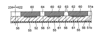
〔形態1 めっき処理によって作製された1層構造を有する蒸着マスク〕
はじめに、蒸着マスク20がめっき処理によって作製された1層構造を有する場合について説明する。図4は、めっき処理によって作製された1層構造の蒸着マスク20を、図3のA−A線に沿って切断した場合を示す断面図である。
[Embodiment 1 Vapor deposition mask having a one-layer structure produced by plating]
First, the case where the vapor deposition mask 20 has a one-layer structure produced by a plating process will be described. FIG. 4 is a cross-sectional view showing a case where the vapor deposition mask 20 having a single layer structure manufactured by plating is cut along the line AA in FIG.

この形態における蒸着マスク20は、図3および図4に示すように、金属層28(マスク本体)と、金属層28に設けられた複数の上述した貫通孔25と、を備えている。   The vapor deposition mask 20 in this embodiment includes a metal layer 28 (mask body) and a plurality of the above-described through holes 25 provided in the metal layer 28 as shown in FIGS. 3 and 4.

このうち金属層28は、インデンテーション弾性率をx(GPa)、0.2%耐力をy(MPa)としたときに、
y≧950、かつ、y≧23x−1280 ・・・(1)
を満たしている。ここで、インデンテーション弾性率とは、極小領域の弾性率を評価するためのナノ・インデンテーション試験によって算出される弾性率である。弾性率の指標としてインデンテーション弾性率を採用することにより、金属層28の厚みが小さい場合であっても、その弾性率を適切に評価することができる。0.2%耐力とは、除荷時の永久ひずみが0.2%となる応力を言う。
Of these, the metal layer 28 has an indentation elastic modulus x (GPa) and a 0.2% proof stress y (MPa).
y ≧ 950 and y ≧ 23x−1280 (1)
Meet. Here, the indentation elastic modulus is an elastic modulus calculated by a nano-indentation test for evaluating the elastic modulus in the minimum region. By adopting the indentation elastic modulus as an index of the elastic modulus, even when the thickness of the metal layer 28 is small, the elastic modulus can be appropriately evaluated. The 0.2% proof stress refers to a stress at which the permanent set upon unloading is 0.2%.

あるいは、金属層28は、インデンテーション弾性率をx(GPa)、インデンテーション硬度をz(GPa)としたときに、
z≧3.7、かつ、z≧0.1x−6.0 ・・・(1)
を満たしている。ここで、インデンテーション硬度とは、上記ナノ・インデンテーション試験によって算出される硬度である。硬度の指標としてインデンテーション硬度を採用することにより、金属層28の厚みが小さい場合であっても、その硬度を適切に評価することができる。
Alternatively, when the metal layer 28 has an indentation elastic modulus x (GPa) and an indentation hardness z (GPa),
z ≧ 3.7 and z ≧ 0.1x−6.0 (1)
Meet. Here, the indentation hardness is a hardness calculated by the nano-indentation test. By adopting indentation hardness as an index of hardness, even when the thickness of the metal layer 28 is small, the hardness can be appropriately evaluated.

ここで、本明細書では、金属層28が上記式(1)を満たしているとは、貫通孔25が形成されていない状態の金属層28が上記式(1)を満たしていることを意味し、貫通孔25が形成された状態の金属層28が上記式(1)を満たしていることを意味するものではない、とする。従って、本明細書では、蒸着マスク20が、上記式(1)を満たしている金属層28に、貫通孔25が形成されたという構成を有している、と言うことができる。貫通孔25が形成された状態の金属層28では、インデンテーション弾性率や0.2%耐力(若しくは、インデンテーション硬度)が、貫通孔25の大きさ、ピッチ、形状等によって影響を受けると考えられる。このため、蒸着マスク20の完成形として、金属層28に複数の貫通孔25が形成された状態においては、上記式(1)を満たす金属層28の領域は、貫通孔25が形成されていない領域、より詳細にはインデンテーション弾性率および0.2%耐力(若しくは、インデンテーション硬度)に貫通孔25の影響が及ばない領域であって、例えば、上述した周囲領域23のうち貫通孔25の影響が及ばない領域や、有効領域22のうち互いに隣り合う貫通孔25同士の間の領域であって貫通孔25の影響が及ばない領域となる。従って、蒸着マスク20の完成形から金属層28のインデンテーション弾性率および0.2%耐力(若しくは、インデンテーション硬度)を調べる場合には、周囲領域23のうち貫通孔25が含まれない領域を切り取って、後述するナノ・インデンテーション試験、および0.2%耐力を調べる場合には引張試験を行うことが好適である。また、有効領域22であっても、互いに隣り合う貫通孔25同士の間の距離が、ナノ・インデンテーション試験、および0.2%耐力を調べる場合の引張試験を行うことが可能な程度の距離であれば、貫通孔25同士の間の領域を切り取ってもよい。なお、材料特性の点で述べると、一般的に蒸着マスク20の金属層28は、材料の組成や材質が位置によって異なることはない。このため、貫通孔25に近い位置と、貫通孔25から離れた位置とで、材料の特性が異なることはない。   Here, in this specification, that the metal layer 28 satisfies the above formula (1) means that the metal layer 28 in a state where the through hole 25 is not formed satisfies the above formula (1). However, it does not mean that the metal layer 28 in the state where the through-holes 25 are formed satisfies the above formula (1). Therefore, in this specification, it can be said that the vapor deposition mask 20 has a configuration in which the through hole 25 is formed in the metal layer 28 that satisfies the above-described formula (1). In the metal layer 28 in the state where the through holes 25 are formed, the indentation elastic modulus and 0.2% proof stress (or indentation hardness) are considered to be affected by the size, pitch, shape, etc. of the through holes 25. It is done. For this reason, in a state where a plurality of through holes 25 are formed in the metal layer 28 as a completed form of the vapor deposition mask 20, the through hole 25 is not formed in the region of the metal layer 28 that satisfies the above formula (1). The region, more specifically, the region where the through hole 25 does not affect the indentation elastic modulus and the 0.2% proof stress (or indentation hardness). This is a region that is not affected, or a region that is between the adjacent through holes 25 in the effective region 22 and that is not affected by the through holes 25. Therefore, when examining the indentation elastic modulus and 0.2% proof stress (or indentation hardness) of the metal layer 28 from the completed form of the vapor deposition mask 20, the region of the surrounding region 23 that does not include the through hole 25 is selected. It is preferable to perform a tensile test when cutting and examining the nano-indentation test described later and the 0.2% proof stress. Further, even in the effective region 22, the distance between the adjacent through holes 25 is such that the nano-indentation test and the tensile test for examining 0.2% proof stress can be performed. If so, the region between the through holes 25 may be cut off. In terms of material properties, the metal layer 28 of the vapor deposition mask 20 generally does not vary in material composition or material depending on the position. For this reason, the characteristics of the material do not differ between a position close to the through hole 25 and a position away from the through hole 25.

蒸着マスク20の貫通孔25は、第1面20a側に位置し、第1面20aにおいて開口寸法S1を有する第1開口部30と、第2面20b側に位置し、第2面20bにおいて開口寸法S2を有する第2開口部35と、を含んでいる。言い換えると、第1面20a側の第1開口部30と第2面20b側の第2開口部35とが互いに連通することにより、貫通孔25が形成されている。図4において、蒸着マスク20の有効領域22のうち、第1面20a側の第1開口部30の輪郭を画定している部分(以下、第1部分とも称する)が符号32で表され、第2面20b側の第2開口部35の輪郭を画定している部分(以下、第2部分とも称する)が符号37で表されている。第1部分32および第2部分37は例えば、後述するめっき処理工程において基材51の表面51a上に析出する金属層28として同時に形成される。   The through hole 25 of the vapor deposition mask 20 is located on the first surface 20a side, is located on the first surface 30a having the opening dimension S1 on the first surface 20a, and on the second surface 20b side, and is opened on the second surface 20b. A second opening 35 having a dimension S2. In other words, the first opening 30 on the first surface 20a side and the second opening 35 on the second surface 20b side communicate with each other, whereby the through hole 25 is formed. In FIG. 4, a portion (hereinafter also referred to as a first portion) demarcating the outline of the first opening 30 on the first surface 20 a side in the effective region 22 of the vapor deposition mask 20 is represented by reference numeral 32. A portion demarcating the outline of the second opening 35 on the two-surface 20b side (hereinafter also referred to as a second portion) is denoted by reference numeral 37. For example, the first portion 32 and the second portion 37 are simultaneously formed as the metal layer 28 deposited on the surface 51a of the substrate 51 in a plating process described later.

図3に示すように、貫通孔25を構成する第1開口部30や第2開口部35は、平面視において略多角形状になっていてもよい。ここでは第1開口部30および第2開口部35が、略四角形状、より具体的には略正方形状になっている例が示されている。また図示はしないが、第1開口部30や第2開口部35は、略六角形状や略八角形状など、その他の略多角形状になっていてもよい。なお「略多角形状」とは、多角形の角部が丸められている形状を含む概念である。また図示はしないが、第1開口部30や第2開口部35は、円形状になっていてもよい。また、平面視において第2開口部35が第1開口部30を囲う輪郭を有する限りにおいて、第1開口部30の形状と第2開口部35の形状が相似形になっている必要はない。   As shown in FIG. 3, the first opening 30 and the second opening 35 constituting the through hole 25 may have a substantially polygonal shape in plan view. Here, an example is shown in which the first opening 30 and the second opening 35 have a substantially square shape, more specifically, a substantially square shape. Although not shown, the first opening 30 and the second opening 35 may have other substantially polygonal shapes such as a substantially hexagonal shape and a substantially octagonal shape. The “substantially polygonal shape” is a concept including a shape in which corners of a polygon are rounded. Although not shown, the first opening 30 and the second opening 35 may be circular. Moreover, as long as the 2nd opening part 35 has the outline which surrounds the 1st opening part 30 in planar view, the shape of the 1st opening part 30 and the shape of the 2nd opening part 35 do not need to be similar.

図5は、図4の金属層28の第1部分32および第2部分37を拡大して示す図である。後述するように、第1部分32は、基材51の低密着性領域56とめっき用レジストパターン60の第1面61との間において析出した金属によって形成される部分である。一方、第2部分37は、めっき用レジストパターン60の隙間64において析出した金属によって形成される部分である。図5においては、第1部分32と第2部分37との間の仮想的な境界線が一点鎖線で示されている。また、第1部分32によって画定される第1開口部30の壁面31と、第2部分37によって画定される第2開口部35の壁面36とが接する接続部が符号40で表されている。なお「壁面31」とは、第1部分32の面のうち第1開口部30を画成する面のことである。上述の「壁面36」も同様に、第2部分37の面のうち第2開口部35を画成する面のことである。   FIG. 5 is an enlarged view showing the first portion 32 and the second portion 37 of the metal layer 28 of FIG. As will be described later, the first portion 32 is a portion formed by a metal deposited between the low adhesion region 56 of the substrate 51 and the first surface 61 of the plating resist pattern 60. On the other hand, the second portion 37 is a portion formed by metal deposited in the gap 64 of the plating resist pattern 60. In FIG. 5, a virtual boundary line between the first portion 32 and the second portion 37 is indicated by a one-dot chain line. In addition, a connection portion where the wall surface 31 of the first opening 30 defined by the first portion 32 and the wall surface 36 of the second opening 35 defined by the second portion 37 are in contact with each other is denoted by reference numeral 40. The “wall surface 31” is a surface that defines the first opening 30 in the surface of the first portion 32. Similarly, the above-mentioned “wall surface 36” is a surface that defines the second opening 35 among the surfaces of the second portion 37.

図5に示すように、蒸着マスク20の第2面20bにおける金属層28の幅M2は、蒸着マスク20の第1面20aにおける金属層28の幅M1よりも小さくなっている。言い換えると、第2面20bにおける貫通孔25(第2開口部35)の開口寸法S2は、第1面20aにおける貫通孔25(第1開口部30)の開口寸法S1よりも大きくなっている。以下、このように金属層28を構成することの利点について説明する。   As shown in FIG. 5, the width M2 of the metal layer 28 on the second surface 20b of the vapor deposition mask 20 is smaller than the width M1 of the metal layer 28 on the first surface 20a of the vapor deposition mask 20. In other words, the opening dimension S2 of the through hole 25 (second opening 35) in the second surface 20b is larger than the opening dimension S1 of the through hole 25 (first opening 30) in the first surface 20a. Hereinafter, advantages of configuring the metal layer 28 in this way will be described.

蒸着マスク20の第2面20b側から飛来する蒸着材料98は、貫通孔25の第2開口部35および第1開口部30を順に通過して有機EL基板92に付着する。有機EL基板92のうち蒸着材料98が付着する領域は、第1面20aにおける貫通孔25の開口寸法S1や開口形状によって主に定められる。ところで、図4において第2面20b側から第1面20aへ向かう矢印L1で示すように、蒸着材料98は、るつぼ94から有機EL基板92に向けて蒸着マスク20の法線方向Nに沿って移動するだけでなく、蒸着マスク20の法線方向Nに対して大きく傾斜した方向に移動することもある。ここで、仮に第2面20bにおける貫通孔25の開口寸法S2が第1面20aにおける貫通孔25の開口寸法S1と同一であるとすると、蒸着マスク20の法線方向Nに対して大きく傾斜した方向に移動する蒸着材料98の多くは、貫通孔25を通過して有機EL基板92に到達するよりも前に、貫通孔25の第2開口部35の壁面36に到達して付着してしまう。従って、蒸着材料98の利用効率を高めるためには、第2開口部35の開口寸法S2を大きくすること、すなわち第2面20b側における金属層28の幅M2を小さくすることが好ましいと言える。   The vapor deposition material 98 flying from the second surface 20 b side of the vapor deposition mask 20 passes through the second opening 35 and the first opening 30 of the through hole 25 in order and adheres to the organic EL substrate 92. A region of the organic EL substrate 92 to which the vapor deposition material 98 adheres is mainly determined by the opening size S1 and the opening shape of the through hole 25 in the first surface 20a. By the way, as shown by an arrow L1 from the second surface 20b side to the first surface 20a in FIG. 4, the vapor deposition material 98 is along the normal direction N of the vapor deposition mask 20 from the crucible 94 toward the organic EL substrate 92. In addition to movement, the vapor deposition mask 20 may move in a direction greatly inclined with respect to the normal direction N of the vapor deposition mask 20. Here, assuming that the opening dimension S2 of the through hole 25 in the second surface 20b is the same as the opening dimension S1 of the through hole 25 in the first surface 20a, it is greatly inclined with respect to the normal direction N of the vapor deposition mask 20. Most of the vapor deposition material 98 that moves in the direction reaches and adheres to the wall surface 36 of the second opening 35 of the through hole 25 before reaching the organic EL substrate 92 through the through hole 25. . Therefore, in order to increase the utilization efficiency of the vapor deposition material 98, it can be said that it is preferable to increase the opening dimension S2 of the second opening 35, that is, to reduce the width M2 of the metal layer 28 on the second surface 20b side.

図4において、第2部分37の端部39および第1部分32の端部34を通る直線L1が、蒸着マスク20の法線方向Nに対してなす角度が、符号θ1で表されている。斜めに移動する蒸着材料98を、第2開口部35の壁面36に到達させることなく可能な限り有機EL基板92に到達させるためには、角度θ1を大きくすることが有利となる。角度θ1を大きくする上では、第1面20a側における金属層28の幅M1に比べて第2面20b側における金属層28の幅M2を小さくすることが有効である。また図から明らかなように、角度θ1を大きくする上では、第1部分32の厚みT1や第2部分37の厚みT2を小さくすることも有効である。ここで「第1部分32の厚みT1」は、第1部分32と第2部分37との境界における第1部分32の厚みを意味している。また図5から明らかなように、第2部分37の厚みT2は、蒸着マスク20の有効領域22を構成する金属層28の厚みと同義である。なお幅M2や厚みT1、厚みT2を過剰に小さくしてしまうと、蒸着マスク20の強度が低下し、このため搬送時や使用時に蒸着マスク20が破損してしまうことが考えられる。例えば、蒸着マスク20をフレーム15に張設する際に蒸着マスク20に加えられる引張り応力によって、蒸着マスク20が破損してしまうことが考えられる。これらの点を考慮すると、蒸着マスク20の各部分の幅や厚みが以下の範囲に設定されることが好ましいと言える。これによって、上述の角度θ1を例えば45°以上にすることができる。   In FIG. 4, an angle formed by a straight line L <b> 1 passing through the end portion 39 of the second portion 37 and the end portion 34 of the first portion 32 with respect to the normal direction N of the vapor deposition mask 20 is represented by reference sign θ <b> 1. In order to make the vapor deposition material 98 moving obliquely reach the organic EL substrate 92 as much as possible without reaching the wall surface 36 of the second opening 35, it is advantageous to increase the angle θ1. In order to increase the angle θ1, it is effective to make the width M2 of the metal layer 28 on the second surface 20b side smaller than the width M1 of the metal layer 28 on the first surface 20a side. As is clear from the figure, it is also effective to reduce the thickness T1 of the first portion 32 and the thickness T2 of the second portion 37 in increasing the angle θ1. Here, “the thickness T 1 of the first portion 32” means the thickness of the first portion 32 at the boundary between the first portion 32 and the second portion 37. Further, as apparent from FIG. 5, the thickness T <b> 2 of the second portion 37 is synonymous with the thickness of the metal layer 28 constituting the effective region 22 of the vapor deposition mask 20. If the width M2, the thickness T1, and the thickness T2 are excessively reduced, the strength of the vapor deposition mask 20 is lowered, and therefore the vapor deposition mask 20 may be damaged during transportation or use. For example, it is conceivable that the vapor deposition mask 20 is damaged due to the tensile stress applied to the vapor deposition mask 20 when the vapor deposition mask 20 is stretched on the frame 15. Considering these points, it can be said that the width and thickness of each portion of the vapor deposition mask 20 are preferably set in the following ranges. Thereby, the above-mentioned angle θ1 can be set to 45 ° or more, for example.

・第1面20a側における金属層28の幅M1:5〜25μm
・第2面20b側における金属層28の幅M2:2〜20μm
・第1部分32の厚みT1:5μm以下
・第2部分37の厚みT2:1〜50μm、より好ましくは3〜30μm、さらに好ましくは3〜25μm、さらに好ましくは3〜15μm
・厚みT1と厚みT2との差ΔT:0.1〜50μm、より好ましくは3〜30μm、さらに好ましくは3〜25μm、さらに好ましくは3〜15μm
とりわけ、第2部分37の厚みT2を15μm以下とすることにより、後述する圧延材で作製された蒸着マスク20では得ることが困難な厚みで蒸着マスク20を作製することができる。この場合、シャドーの影響を低減し、蒸着材料の利用効率を向上させることが可能な蒸着マスク20を得ることができる。
The width M1 of the metal layer 28 on the first surface 20a side is from 1 to 25 μm.
The width M2 of the metal layer 28 on the second surface 20b side: 2 to 20 μm
-Thickness T1 of the first portion 32: 5 [mu] m or less-Thickness T2 of the second portion 37: 1-50 [mu] m, more preferably 3-30 [mu] m, still more preferably 3-25 [mu] m, still more preferably 3-15 [mu] m
Difference ΔT between thickness T1 and thickness T2: 0.1 to 50 μm, more preferably 3 to 30 μm, still more preferably 3 to 25 μm, still more preferably 3 to 15 μm
In particular, by setting the thickness T2 of the second portion 37 to 15 μm or less, the vapor deposition mask 20 can be produced with a thickness that is difficult to obtain with the vapor deposition mask 20 produced from a rolled material described later. In this case, it is possible to obtain the vapor deposition mask 20 capable of reducing the influence of shadow and improving the utilization efficiency of the vapor deposition material.

表1に、5インチの有機EL表示装置において、表示画素数、および表示画素数に応じて求められる、蒸着マスク20の各部分の幅や厚みの値の例を示す。なお「FHD」は、Full High Definitionを意味し、「WQHD」は、Wide Quad High Definitionを意味し、「UHD」は、Ultra High Definitionを意味している。

Figure 0006443457
Table 1 shows an example of values of the width and thickness of each part of the vapor deposition mask 20 which are obtained according to the number of display pixels and the number of display pixels in a 5-inch organic EL display device. “FHD” means Full High Definition, “WQHD” means Wide Quad High Definition, and “UHD” means Ultra High Definition.
Figure 0006443457

次に、第1部分32の形状についてより詳細に説明する。仮に図5において点線で示すように、端部34において第1部分32が、第2面20b側へ向かって大きく切り立った形状を有している場合、貫通孔25の第2開口部35を通過した後の蒸着材料98の多くが第1部分32の壁面31に到達して付着してしまうことが考えられる。このような、端部34近傍における第1部分32への蒸着材料98の付着を抑制するため、図5に示すように、第1部分32は、端部34およびその近傍において、第1部分32のうち第2部分37に接する部分における厚みT1よりも小さな厚みを有することが好ましい。例えば図5に示すように、第1部分32の厚みが、第1部分32のうち第2部分37に接する部分から端部34に向かうにつれて単調に減少していることが好ましい。このような第1部分32の形状は、後述するように、めっき処理によって第1部分32を形成することによって実現され得る。   Next, the shape of the first portion 32 will be described in more detail. As shown by a dotted line in FIG. 5, when the first portion 32 has a shape that is greatly cut toward the second surface 20 b side at the end portion 34, it passes through the second opening 35 of the through hole 25. It is conceivable that most of the deposited material 98 after reaching the wall surface 31 of the first portion 32 adheres. In order to suppress the adhesion of the vapor deposition material 98 to the first portion 32 in the vicinity of the end portion 34 as described above, as shown in FIG. 5, the first portion 32 includes the first portion 32 at the end portion 34 and in the vicinity thereof. Of these, it is preferable to have a thickness smaller than the thickness T1 in the portion in contact with the second portion 37. For example, as shown in FIG. 5, it is preferable that the thickness of the first portion 32 monotonously decreases from the portion of the first portion 32 that contacts the second portion 37 toward the end portion 34. Such a shape of the first portion 32 can be realized by forming the first portion 32 by plating as described later.

(蒸着マスクの製造方法)
次に、以上のような構成からなる蒸着マスク20を製造する方法について、図6〜図13Bを参照して説明する。
(Method for manufacturing vapor deposition mask)
Next, a method of manufacturing the vapor deposition mask 20 having the above configuration will be described with reference to FIGS.

まず、後述する基材51上に、めっき処理によって、貫通孔25が設けられた金属層28(マスク本体)を形成する工程(成膜工程)が実施される。当該成膜工程は、後述する準備工程と、表面処理用レジスト形成工程と、表面処理工程と、めっき用レジスト形成工程と、めっき処理工程と、を有している。   First, a step (film formation step) of forming a metal layer 28 (mask main body) provided with the through holes 25 on a base material 51 described later is performed by plating. The film formation step includes a preparation step, a surface treatment resist formation step, a surface treatment step, a plating resist formation step, and a plating treatment step which will be described later.

(準備工程)
はじめに図6に示すように、めっき処理の際の下地となる基材51を準備する準備工程を実施する。ここでは、めっき処理が電解めっき処理である例について説明する。この場合、基材51の表面51aのうち少なくとも金属層28が析出する部分は、導電性を有する導電層によって構成されている。例えば基材51全体が、導電性を有する導電層によって構成されていてもよい。この場合、基材51のうち表面51aの反対側に位置する裏面51bには、裏面51bが他の部材と導通してしまうことを防ぐための、絶縁性を有するカバーフィルム52が設けられていてもよい。
(Preparation process)
First, as shown in FIG. 6, a preparatory process for preparing a base material 51 that is a base for the plating process is performed. Here, an example in which the plating process is an electrolytic plating process will be described. In this case, at least a portion of the surface 51a of the substrate 51 where the metal layer 28 is deposited is constituted by a conductive layer having conductivity. For example, the whole base material 51 may be comprised by the conductive layer which has electroconductivity. In this case, an insulating cover film 52 for preventing the back surface 51b from being electrically connected to other members is provided on the back surface 51b located on the opposite side of the front surface 51a of the base material 51. Also good.

後述するめっき処理の際に所定の金属を析出させることができる限りにおいて、基材51の導電層を構成する材料が特に限られることはない。例えば、基材51の導電層を構成する材料としては、金属材料や酸化物導電性材料等の導電性を有する材料が適宜用いられる。金属材料の例としては、例えばステンレススチールや銅などを挙げることができる。好ましくは、後述するめっき用レジストパターン60に対する高い密着性を有する材料が、基材51の導電層を構成する材料として用いられる。例えばめっき用レジストパターン60が、アクリル系光硬化性樹脂を含むレジスト膜など、いわゆるドライフィルムと称されるものをパターニングすることによって作製される場合、基材51の導電層を構成する材料として、ドライフィルムに対する高い密着性を有する銅が用いられることが好ましい。   As long as a predetermined metal can be deposited in the later-described plating process, the material constituting the conductive layer of the substrate 51 is not particularly limited. For example, as a material constituting the conductive layer of the substrate 51, a conductive material such as a metal material or an oxide conductive material is appropriately used. Examples of the metal material include stainless steel and copper. Preferably, a material having high adhesion to a plating resist pattern 60 described later is used as a material constituting the conductive layer of the substrate 51. For example, when the resist pattern 60 for plating is produced by patterning a so-called dry film such as a resist film containing an acrylic photocurable resin, as a material constituting the conductive layer of the substrate 51, It is preferable to use copper having high adhesion to a dry film.

準備工程においては、基材51を準備した後、基材51の表面51aに高密着性領域55および低密着性領域56を形成する工程を実施する。ここで「高密着性領域55および低密着性領域56」は、高密着性領域55に対する、後述するめっき用レジストパターン60の第1面61の密着力が、低密着性領域56に対するめっき用レジストパターン60の第1面61の密着力よりも相対的に高くなるよう構成された領域として定義される。図9Aおよび図9Bは、高密着性領域55および低密着性領域56が形成された基材51を示す断面図および平面図である。高密着性領域55は、めっき処理によって基材51の表面51a上に作製される蒸着マスク20の第1面20a側の第1開口部30に対応する領域である。図9Aおよび図9Bに示すように、高密着性領域55は、基材51の表面51a上に複数形成される。また各高密着性領域55は、第1開口部30に対応する形状、例えば略矩形形状を有している。一方、低密着性領域56は、各高密着性領域55を取り囲むよう形成される。高密着性領域55および低密着性領域56とめっき用レジストパターン60との間の密着力の評価方法としては、例えば、JIS K5400−8に記載の碁盤目試験、JIS−5600−5−6に記載のクロスカット法、JIS K5600−5−7に記載のプルオフ法などを用いることができる。   In the preparation step, after preparing the substrate 51, a step of forming the high adhesion region 55 and the low adhesion region 56 on the surface 51 a of the substrate 51 is performed. Here, the “high adhesion region 55 and the low adhesion region 56” means that the adhesion force of the first surface 61 of the plating resist pattern 60 to be described later to the high adhesion region 55 is a plating resist for the low adhesion region 56. It is defined as a region configured to be relatively higher than the adhesion force of the first surface 61 of the pattern 60. 9A and 9B are a cross-sectional view and a plan view showing the substrate 51 on which the high adhesion region 55 and the low adhesion region 56 are formed. The high adhesion region 55 is a region corresponding to the first opening 30 on the first surface 20a side of the vapor deposition mask 20 produced on the surface 51a of the substrate 51 by plating. As shown in FIGS. 9A and 9B, a plurality of high adhesion regions 55 are formed on the surface 51 a of the substrate 51. Each high adhesion region 55 has a shape corresponding to the first opening 30, for example, a substantially rectangular shape. On the other hand, the low adhesion region 56 is formed so as to surround each high adhesion region 55. As a method for evaluating the adhesion between the high adhesion region 55 and the low adhesion region 56 and the resist pattern 60 for plating, for example, a cross-cut test described in JIS K5400-8, JIS-5600-5-6 A cross-cut method described in the above, a pull-off method described in JIS K5600-5-7, or the like can be used.

(表面処理用レジスト形成工程)
以下、基材51上に高密着性領域55および低密着性領域56を形成する方法の一例について、図7および図8を参照して説明する。はじめに図7に示すように、基材51の表面51aのうち低密着性領域56に対応する領域の上に表面処理用レジストパターン53を形成する表面処理用レジスト形成工程を実施する。言い換えると、基材51の表面51aのうち高密着性領域55に対応する領域に隙間53aが空けられるよう、基材51の表面51a上に表面処理用レジストパターン53を設ける。具体的には、はじめに、基材51の表面51aにドライフィルムを貼り付けることによって、ネガ型のレジスト膜を形成する。ドライフィルムの例としては、例えば日立化成製のRY3310など、アクリル系光硬化性樹脂を含むものを挙げることができる。次に、レジスト膜のうち隙間53aとなるべき領域に光を透過させないようにした露光マスクを準備し、露光マスクをレジスト膜上に配置する。その後、真空密着によって露光マスクをレジスト膜に十分に密着させる。なおレジスト膜として、ポジ型のものが用いられてもよい。この場合、露光マスクとして、レジスト膜のうちの除去したい領域に光を透過させるようにした露光マスクが用いられる。
(Surface treatment resist formation process)
Hereinafter, an example of a method for forming the high adhesion region 55 and the low adhesion region 56 on the substrate 51 will be described with reference to FIGS. 7 and 8. First, as shown in FIG. 7, a surface treatment resist forming step is performed in which a surface treatment resist pattern 53 is formed on a region corresponding to the low adhesion region 56 on the surface 51 a of the substrate 51. In other words, the surface treatment resist pattern 53 is provided on the surface 51 a of the substrate 51 so that a gap 53 a is formed in a region corresponding to the high adhesion region 55 in the surface 51 a of the substrate 51. Specifically, first, a negative resist film is formed by attaching a dry film to the surface 51a of the base material 51. Examples of the dry film include those containing an acrylic photocurable resin such as RY3310 manufactured by Hitachi Chemical. Next, an exposure mask is prepared so as not to transmit light to the region of the resist film that should become the gap 53a, and the exposure mask is disposed on the resist film. Thereafter, the exposure mask is sufficiently adhered to the resist film by vacuum adhesion. Note that a positive type resist film may be used. In this case, an exposure mask in which light is transmitted through a region to be removed of the resist film is used as the exposure mask.

その後、レジスト膜を露光マスク越しに露光する。さらに、露光されたレジスト膜に像を形成するためにレジスト膜を現像する。以上のようにして、図7に示す表面処理用レジストパターン53を形成することができる。なお、表面処理用レジストパターン53を基材51の表面51aに対してより強固に密着させるため、現像工程の後に表面処理用レジストパターン53を加熱する熱処理工程を実施してもよい。   Thereafter, the resist film is exposed through an exposure mask. Further, the resist film is developed to form an image on the exposed resist film. As described above, the resist pattern 53 for surface treatment shown in FIG. 7 can be formed. In order to make the surface treatment resist pattern 53 tightly adhere to the surface 51a of the substrate 51, a heat treatment step of heating the surface treatment resist pattern 53 may be performed after the development step.

(表面処理工程)
次に、図8に示すように、基材51の表面51aのうち表面処理用レジストパターン53によって覆われていない領域を表面処理して被処理領域54を形成する表面処理工程を実施する。ここでは、表面処理液として、基材51の表面51aをソフトエッチングすることによって表面51aを粗化することができるものが用いられる。例えば表面処理液として、過酸化水素水および硫酸を含む、いわゆる過酸化水素/硫酸系のソフトエッチング剤などが用いられ、具体的にはAtoteck社製のボンドフィルムなどが用いられ得る。このような表面処理液を用いて基材51の表面51aを部分的に粗化することにより、後述するめっき用レジストパターン60に対する表面51aの被処理領域54の密着力を部分的に高めることができる。すなわち、表面処理液によって表面処理された被処理領域54が、めっき用レジストパターン60に対する高い密着力を有する高密着性領域55となる。また、表面処理用レジストパターン53によって覆われているために表面処理が施されなかった領域が、めっき用レジストパターン60に対する密着力が高密着性領域55に比べて相対的に低い低密着性領域56となる。高密着性領域55に施される粗化処理の程度、例えば高密着性領域55の表面粗さは、高密着性領域55を構成する材料や後述するめっき用レジストパターン60を構成する材料などに応じて適宜定められる。例えば、菱化システム社製の走査型白色干渉計VertScanを用いて表面粗さを測定した場合、高密着性領域55および低密着性領域56における表面粗さはそれぞれ以下の範囲内になっている。

Figure 0006443457
なお表2において、「表面積率(s-ratio)」は、高密着性領域55や低密着性領域56の表面の起伏や凹凸を考慮しない、表面の二次元的な投影面積に対する、高密着性領域55や低密着性領域56の表面の起伏や凹凸を含めた、表面の三次元的な実測面積の比を意味している。(Surface treatment process)
Next, as shown in FIG. 8, a surface treatment process is performed in which a region of the surface 51 a of the substrate 51 that is not covered with the surface treatment resist pattern 53 is surface-treated to form a treatment region 54. Here, a surface treatment liquid that can roughen the surface 51a by soft etching the surface 51a of the substrate 51 is used. For example, a so-called hydrogen peroxide / sulfuric acid based soft etching agent containing hydrogen peroxide and sulfuric acid is used as the surface treatment liquid, and specifically, a bond film manufactured by Atoteck or the like can be used. By partially roughening the surface 51a of the substrate 51 using such a surface treatment liquid, it is possible to partially increase the adhesion of the treated region 54 of the surface 51a to the plating resist pattern 60 described later. it can. That is, the region 54 to be treated which has been surface-treated with the surface treatment liquid becomes a high adhesion region 55 having a high adhesion to the plating resist pattern 60. Further, the region that is not subjected to the surface treatment because it is covered with the surface treatment resist pattern 53 is a low adhesion region in which the adhesion force to the plating resist pattern 60 is relatively lower than that of the high adhesion region 55. 56. The degree of the roughening treatment applied to the high adhesion region 55, for example, the surface roughness of the high adhesion region 55, depends on the material constituting the high adhesion region 55 or the material constituting the plating resist pattern 60 described later. It is determined accordingly. For example, when the surface roughness is measured using a scanning white interferometer VertScan manufactured by Ryoka System, the surface roughness in the high adhesion region 55 and the low adhesion region 56 is within the following ranges, respectively. .
Figure 0006443457
In Table 2, “surface area ratio (s-ratio)” indicates the high adhesion to the two-dimensional projected area of the surface without taking into account the undulations and irregularities of the surface of the high adhesion region 55 and the low adhesion region 56. It means the ratio of the three-dimensional measured area of the surface including the undulations and irregularities on the surface of the region 55 and the low adhesion region 56.

なお、めっき用レジストパターン60に対する基材51の表面51aの密着力を部分的に高めることができる限りにおいて、表面処理工程の内容が、上述の粗化処理に限られることはない。例えば表面処理工程は、めっき用レジストパターン60に対する高い密着性を有する層を、基材51の表面51aのうち表面処理用レジストパターン53によって覆われていない領域に設ける工程であってもよい。   Note that the content of the surface treatment process is not limited to the above-described roughening treatment as long as the adhesion of the surface 51a of the substrate 51 to the plating resist pattern 60 can be partially enhanced. For example, the surface treatment step may be a step of providing a layer having high adhesion to the plating resist pattern 60 in a region of the surface 51 a of the substrate 51 that is not covered with the surface treatment resist pattern 53.

その後、表面処理用レジストパターン53を除去する除去工程を実施する。例えばアルカリ系剥離液を用いることによって、表面処理用レジストパターン53を基材51の表面51aから剥離させることができる。このようにして、図9Aおよび図9Bに示すように、複数の高密着性領域55と、高密着性領域55を取り囲む低密着性領域56と、に区画された表面51aを有する基材51を準備することができる。   Thereafter, a removing step for removing the surface treatment resist pattern 53 is performed. For example, the surface treatment resist pattern 53 can be peeled from the surface 51 a of the substrate 51 by using an alkaline stripping solution. In this way, as shown in FIGS. 9A and 9B, the base material 51 having the surface 51a partitioned into a plurality of high adhesion regions 55 and a low adhesion region 56 surrounding the high adhesion regions 55. Can be prepared.

(めっき用レジスト形成工程)
次に、基材51の表面51a上に、所定の隙間64を空けてめっき用レジストパターン60を形成するめっき用レジスト形成工程を実施する。図10Aおよび図10Bは、めっき用レジストパターン60が形成された基材51を示す断面図および平面図である。図10Aに示すように、めっき用レジストパターン60は、基材51の表面51aに対向する第1面61と、第1面61の反対側に位置する第2面62と、隙間64に面する側面63と、を含んでいる。
(Plating resist formation process)
Next, a plating resist forming step for forming a plating resist pattern 60 on the surface 51a of the substrate 51 with a predetermined gap 64 is performed. 10A and 10B are a cross-sectional view and a plan view showing the substrate 51 on which the plating resist pattern 60 is formed. As shown in FIG. 10A, the plating resist pattern 60 faces the first surface 61 facing the surface 51 a of the substrate 51, the second surface 62 located on the opposite side of the first surface 61, and the gap 64. Side surface 63.

めっき用レジスト形成工程は、図10Aおよび図10Bに示すように、めっき用レジストパターン60の第1面61が高密着性領域55を覆うとともに低密着性領域56にまで広がり、かつ、めっき用レジストパターン60の隙間64が低密着性領域56上に位置するよう、実施される。この場合、図10Aに示すように、めっき用レジストパターン60の第1面61は、高密着性領域55および低密着性領域56の両方に接し、まためっき用レジストパターン60の側面63は低密着性領域56に接するようになる。なお上述のように高密着性領域55には粗化処理が施されているので、高密着性領域55に対するめっき用レジストパターン60の密着力は、低密着性領域56に対するめっき用レジストパターン60の密着力よりも高くなっている。   In the plating resist forming step, as shown in FIGS. 10A and 10B, the first surface 61 of the plating resist pattern 60 covers the high adhesion region 55 and extends to the low adhesion region 56, and the plating resist It implements so that the clearance gap 64 of the pattern 60 may be located on the low-adhesion area | region 56. FIG. In this case, as shown in FIG. 10A, the first surface 61 of the plating resist pattern 60 is in contact with both the high adhesion region 55 and the low adhesion region 56, and the side surface 63 of the plating resist pattern 60 is low adhesion. It comes into contact with the sex region 56. Since the high adhesion region 55 is roughened as described above, the adhesion force of the plating resist pattern 60 to the high adhesion region 55 is the same as that of the plating resist pattern 60 to the low adhesion region 56. It is higher than the adhesion.

後述するように、蒸着マスク20の第1部分32は、低密着性領域56とめっき用レジストパターン60との間に浸入しためっき液によって形成される。めっき用レジストパターン60のうち高密着性領域55から低密着性領域56へはみ出している部分の幅kは、第1面20a上における第1部分32の幅M3に対応しており、例えば0.5〜5.0μmの範囲内になっている。   As will be described later, the first portion 32 of the vapor deposition mask 20 is formed by a plating solution that has entered between the low adhesion region 56 and the resist pattern 60 for plating. The width k of the portion of the plating resist pattern 60 that protrudes from the high adhesion region 55 to the low adhesion region 56 corresponds to the width M3 of the first portion 32 on the first surface 20a. It is in the range of 5 to 5.0 μm.

めっき用レジスト形成工程においては、上述の表面処理用レジスト形成の場合と同様に、はじめに、基材51の表面51aにドライフィルムを貼り付けることによって、ネガ型のレジスト膜を形成する。ドライフィルムの例としては、例えば日立化成製のRY3310など、アクリル系光硬化性樹脂を含むものを挙げることができる。次に、レジスト膜のうち隙間64となるべき領域に光を透過させないようにした露光マスクを準備し、露光マスクをレジスト膜上に配置する。その後、真空密着によって露光マスクをレジスト膜に十分に密着させる。なおレジスト膜として、ポジ型のものが用いられてもよい。この場合、露光マスクとして、レジスト膜のうちの除去したい領域に光を透過させるようにした露光マスクが用いられる。   In the plating resist formation step, as in the case of the above-described surface treatment resist formation, first, a negative resist film is formed by attaching a dry film to the surface 51a of the base 51. Examples of the dry film include those containing an acrylic photocurable resin such as RY3310 manufactured by Hitachi Chemical. Next, an exposure mask that prevents light from being transmitted to a region that should become the gap 64 in the resist film is prepared, and the exposure mask is disposed on the resist film. Thereafter, the exposure mask is sufficiently adhered to the resist film by vacuum adhesion. Note that a positive type resist film may be used. In this case, an exposure mask in which light is transmitted through a region to be removed of the resist film is used as the exposure mask.

その後、レジスト膜を露光マスク越しに露光する。さらに、露光されたレジスト膜に像を形成するためにレジスト膜を現像する。以上のようにして、図10Aおよび図10Bに示すめっき用レジストパターン60を形成することができる。なお、めっき用レジストパターン60を基材51の表面51aに対して、特に高密着性領域55に対してより強固に密着させるため、現像工程の後にめっき用レジストパターン60を加熱する熱処理工程を実施してもよい。また現像工程の後、酸性の溶液などを用いてめっき用レジストパターン60に囲まれた低密着性領域56の金属表面を活性化する活性化工程を実施してもよい。これによって、めっき用レジストパターン60と低密着性領域56との間の密着性をより低くすることができる。酸性の溶液としては、例えばスルファミン酸を用いることができる。   Thereafter, the resist film is exposed through an exposure mask. Further, the resist film is developed to form an image on the exposed resist film. As described above, the plating resist pattern 60 shown in FIGS. 10A and 10B can be formed. In addition, in order to make the resist pattern 60 for plating adhere more firmly to the surface 51a of the base material 51, particularly to the high adhesion region 55, a heat treatment process for heating the resist pattern 60 for plating is performed after the development process. May be. Moreover, you may implement the activation process of activating the metal surface of the low-adhesion area | region 56 surrounded by the resist pattern 60 for plating using an acidic solution etc. after a image development process. Thereby, the adhesion between the plating resist pattern 60 and the low adhesion region 56 can be further reduced. As the acidic solution, for example, sulfamic acid can be used.

(めっき処理工程)
次に、めっき用レジストパターン60の隙間64にめっき液を供給するめっき処理工程を実施する。例えば、めっき用レジストパターン60が設けられた基材51を、めっき液が充填されためっき槽に浸してもよい。これによって、図11に示すように、隙間64において基材51の表面51a上に金属層28を析出させることができる。
(Plating process)
Next, a plating process step of supplying a plating solution to the gap 64 of the plating resist pattern 60 is performed. For example, the substrate 51 provided with the plating resist pattern 60 may be immersed in a plating tank filled with a plating solution. As a result, as shown in FIG. 11, the metal layer 28 can be deposited on the surface 51 a of the substrate 51 in the gap 64.

基材51の表面51a上に金属層28を析出させることができる限りにおいて、めっき処理工程の具体的な方法が特に限られることとはない。例えば、めっき処理工程は、基材51の導電層に電流を流すことによって基材51の表面51aの低密着性領域56上に金属層28を析出させる、いわゆる電解めっき処理工程として実施されてもよい。若しくは、めっき処理工程は、無電解めっき処理工程であってもよい。なおめっき処理工程が無電解めっき処理工程である場合、基材51の導電層上には適切な触媒層が設けられる。電解めっき処理工程が実施される場合にも、基材51の導電層上に触媒層が設けられていてもよい。   As long as the metal layer 28 can be deposited on the surface 51a of the substrate 51, the specific method of the plating process is not particularly limited. For example, the plating process may be performed as a so-called electrolytic plating process in which the metal layer 28 is deposited on the low adhesion region 56 of the surface 51a of the substrate 51 by passing an electric current through the conductive layer of the substrate 51. Good. Alternatively, the plating process may be an electroless plating process. When the plating process is an electroless plating process, an appropriate catalyst layer is provided on the conductive layer of the substrate 51. Even when the electrolytic plating treatment step is performed, a catalyst layer may be provided on the conductive layer of the substrate 51.

用いられるめっき液の成分は、金属層28に求められる特性に応じて適宜定められる。例えば金属層28が、ニッケルを含む鉄合金によって構成される場合、めっき液として、ニッケル化合物を含む溶液と、鉄化合物を含む溶液との混合溶液を用いることができる。例えば、スルファミン酸ニッケルや臭化ニッケルを含む溶液と、スルファミン酸第一鉄を含む溶液との混合溶液を用いることができる。めっき液には、様々な添加剤が含まれていてもよい。添加剤としては、例えば、ホウ酸などのph緩衝剤や、マロン酸やサッカリンなどの添加剤が含まれていてもよい。その他にも、金属層28を構成する材料に応じて、例えば、ニッケルおよびコバルトを含むめっき液や、ニッケルを含むめっき液などを用いることができる。   The components of the plating solution used are appropriately determined according to the characteristics required for the metal layer 28. For example, when the metal layer 28 is made of an iron alloy containing nickel, a mixed solution of a solution containing a nickel compound and a solution containing an iron compound can be used as the plating solution. For example, a mixed solution of a solution containing nickel sulfamate or nickel bromide and a solution containing ferrous sulfamate can be used. Various additives may be contained in the plating solution. As the additive, for example, a ph buffer such as boric acid or an additive such as malonic acid or saccharin may be contained. In addition, according to the material which comprises the metal layer 28, the plating solution containing nickel and cobalt, the plating solution containing nickel, etc. can be used, for example.

ところで上述のように、めっき用レジストパターン60の隙間64は基材51の低密着性領域56上に位置している。まためっき用レジストパターン60は、高密着性領域55から低密着性領域56へはみ出している。この場合、めっき用レジストパターン60の隙間64に供給されためっき液は、低密着性領域56とめっき用レジストパターン60の第1面61との間にも浸入し得る。このようなめっき液の浸入が生じるため、図11に示すように、隙間64だけでなく、基材51の低密着性領域56とめっき用レジストパターン60の第1面61との間においても金属(金属層28)の析出が生じる。このため、めっき処理工程によって基材51の表面51a上に生じる金属層28は、めっき用レジストパターン60の隙間64において析出した金属によって形成される第2部分37に加えて、基材51の低密着性領域56とめっき用レジストパターン60の第1面61との間において析出した金属によって形成される第1部分32を含むようになる。一方、高密着性領域55においては粗化処理によってめっき用レジストパターン60に対する密着力が高められている。このため図11に示すように、めっき液の浸入を高密着性領域55によって食い止めることができる。このため、金属層28に上述の第1開口部30を確保することができる。   By the way, as described above, the gap 64 of the plating resist pattern 60 is located on the low adhesion region 56 of the substrate 51. Further, the plating resist pattern 60 protrudes from the high adhesion region 55 to the low adhesion region 56. In this case, the plating solution supplied to the gap 64 of the plating resist pattern 60 can also enter between the low adhesion region 56 and the first surface 61 of the plating resist pattern 60. Since such infiltration of the plating solution occurs, as shown in FIG. 11, not only the gap 64 but also the metal between the low adhesion region 56 of the substrate 51 and the first surface 61 of the plating resist pattern 60. Precipitation of (metal layer 28) occurs. For this reason, the metal layer 28 generated on the surface 51a of the base material 51 by the plating process is not limited to the second portion 37 formed by the metal deposited in the gaps 64 of the plating resist pattern 60. The first portion 32 formed by the deposited metal between the adhesive region 56 and the first surface 61 of the plating resist pattern 60 is included. On the other hand, in the high adhesion region 55, the adhesion to the plating resist pattern 60 is enhanced by the roughening treatment. Therefore, as shown in FIG. 11, the penetration of the plating solution can be stopped by the high adhesion region 55. For this reason, the first opening 30 described above can be secured in the metal layer 28.

このようにして、図4および図5に示す金属層28が得られる。   In this way, the metal layer 28 shown in FIGS. 4 and 5 is obtained.

(除去工程)
その後、図12に示すように、めっき用レジストパターン60を金属層28から除去する除去工程を実施する。例えばアルカリ系剥離液を用いることによって、めっき用レジストパターン60を基材51の表面51aから剥離させることができる。めっき用レジストパターン60が除去されることにより、貫通孔25が現れ、貫通孔25が設けられた金属層28を得ることができる。
(Removal process)
Thereafter, as shown in FIG. 12, a removing step of removing the plating resist pattern 60 from the metal layer 28 is performed. For example, the plating resist pattern 60 can be peeled from the surface 51 a of the substrate 51 by using an alkaline stripping solution. By removing the plating resist pattern 60, the through hole 25 appears, and the metal layer 28 provided with the through hole 25 can be obtained.

(分離工程)
次に、金属層28を基材51の表面51aから分離させる分離工程を実施する。これによって、図13Aに示すように、第1面20aから第2面20bまで延びる第2部分37と、第1面20a側において第2部分37から貫通孔25の中心側に向かって広がる第1部分32と、を含む金属層28を有する蒸着マスク20を得ることができる。図13Bは、蒸着マスク20を第2面20b側から見た場合を示す平面図である。
(Separation process)
Next, a separation process for separating the metal layer 28 from the surface 51 a of the substrate 51 is performed. Accordingly, as shown in FIG. 13A, the second portion 37 extending from the first surface 20a to the second surface 20b, and the first portion spreading from the second portion 37 toward the center of the through hole 25 on the first surface 20a side. The vapor deposition mask 20 having the metal layer 28 including the portion 32 can be obtained. FIG. 13B is a plan view showing the case where the vapor deposition mask 20 is viewed from the second surface 20b side.

以下、分離工程の一例について詳細に説明する。はじめに、粘着性を有する物質が塗工などによって設けられているフィルムを、基材51上に形成された金属層28に貼り付ける。次に、フィルムを引き上げたり巻き取ったりすることにより、フィルムを基材51から引き離し、これによって、金属層28を基材51から分離させる。その後、金属層28からフィルムを剥がす。   Hereinafter, an example of the separation step will be described in detail. First, a film in which a substance having adhesiveness is provided by coating or the like is attached to the metal layer 28 formed on the substrate 51. Next, by pulling up or winding up the film, the film is pulled away from the base material 51, thereby separating the metal layer 28 from the base material 51. Thereafter, the film is peeled off from the metal layer 28.

なお粘着性を有する物質としては、UVなどの光を照射されることによって、または加熱されることによって粘着性を喪失する物質を使用してもよい。この場合、金属層28を基材51から分離させた後、フィルムに光を照射する工程やフィルムを加熱する工程を実施する。これによって、金属層28からフィルムを剥がす工程を容易化することができる。例えば、フィルムと金属層28とを可能な限り互いに平行な状態に維持した状態で、フィルムを剥がすことができる。これによって、フィルムを剥がす際に金属層28が湾曲することを抑制することができ、このことにより、蒸着マスク20に湾曲などの変形のくせがついてしまうことを抑制することができる。   Note that as the substance having adhesiveness, a substance that loses adhesiveness when irradiated with light such as UV or when heated may be used. In this case, after separating the metal layer 28 from the base material 51, a step of irradiating the film with light and a step of heating the film are performed. Thereby, the process of peeling the film from the metal layer 28 can be facilitated. For example, the film can be peeled off while keeping the film and the metal layer 28 as parallel as possible. Thereby, it is possible to suppress the metal layer 28 from being bent when the film is peeled off, and thereby it is possible to suppress the deposition mask 20 from being deformed such as a curve.

上述した形態1によれば、上述のように、めっき用レジスト形成工程は、めっき用レジストパターン60が高密着性領域55を覆うとともに低密着性領域56にまで広がり、かつ、めっき用レジストパターン60の隙間64が低密着性領域56上に位置するよう、実施される。このため、めっき処理工程の際、低密着性領域56とめっき用レジストパターン60との間にめっき液を少なくとも部分的に浸入させることができる。これによって、金属層28は、基材51の低密着性領域56とめっき用レジストパターン60との間において析出した金属によって形成される第1部分32と、めっき用レジストパターン60の隙間64において析出した金属によって形成される第2部分37と、を含むようになる。この場合、蒸着マスク20の貫通孔25の形状は、第1面20aにおいては第1部分32によって画定され、第2面20bにおいては第2部分37によって画定される。従って、複雑な形状を有する貫通孔25を得ることができる。   According to the above-described embodiment 1, as described above, in the plating resist formation step, the plating resist pattern 60 covers the high adhesion region 55 and extends to the low adhesion region 56, and the plating resist pattern 60 is formed. The gap 64 is located on the low adhesion region 56. For this reason, the plating solution can be at least partially infiltrated between the low adhesion region 56 and the plating resist pattern 60 during the plating process. As a result, the metal layer 28 is deposited in the first portion 32 formed by the deposited metal between the low adhesion region 56 of the substrate 51 and the plating resist pattern 60 and the gap 64 between the plating resist pattern 60. And a second portion 37 formed of the above-mentioned metal. In this case, the shape of the through hole 25 of the vapor deposition mask 20 is defined by the first portion 32 on the first surface 20a and is defined by the second portion 37 on the second surface 20b. Therefore, the through hole 25 having a complicated shape can be obtained.

また、低密着性領域56とめっき用レジストパターン60との間に浸入しためっき液を利用して第2部分を形成することにより、小さな厚みを有する第1部分32を得ることができる。さらに、第1部分32の厚みを、第1部分32のうち第2部分37に接する部分から端部34に向かうにつれて単調に減少させることも可能になる。これによって、有機EL基板92に到達し得る蒸着材料98の飛来角度に対応する上述の角度θ1を効率的に大きくすることができる。   In addition, the first portion 32 having a small thickness can be obtained by forming the second portion using a plating solution that has entered between the low adhesion region 56 and the resist pattern 60 for plating. Furthermore, the thickness of the first portion 32 can be monotonously decreased from the portion of the first portion 32 that contacts the second portion 37 toward the end portion 34. Thereby, the above-described angle θ1 corresponding to the flying angle of the vapor deposition material 98 that can reach the organic EL substrate 92 can be efficiently increased.

また、めっき処理を利用して金属層28を形成することにより、貫通孔25の形状とは独立に、蒸着マスク20の厚みを任意に設定することができる。このため、十分な強度を蒸着マスク20に持たせることができる。従って、高精細な有機EL表示装置を製造することができ、かつ耐久性に優れた蒸着マスク20を提供することができる。   Moreover, the thickness of the vapor deposition mask 20 can be arbitrarily set independently of the shape of the through-hole 25 by forming the metal layer 28 using a plating process. For this reason, the vapor deposition mask 20 can have sufficient strength. Therefore, a high-definition organic EL display device can be manufactured, and the vapor deposition mask 20 excellent in durability can be provided.

〔形態2 めっき処理によって作製された2層構造を有する蒸着マスク〕
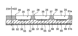
次に、蒸着マスク20がめっき処理によって作製された2層構造を有する場合について説明する。図14は、めっき処理によって作製された2層構造の蒸着マスク20を、図3のA−A線に沿って切断した場合を示す断面図である。
[Form 2: Evaporation mask having a two-layer structure produced by plating]
Next, the case where the vapor deposition mask 20 has a two-layer structure produced by plating is described. FIG. 14 is a cross-sectional view showing a case where the vapor deposition mask 20 having a two-layer structure produced by plating is cut along the line AA in FIG.

この形態における蒸着マスク20は、図14に示すように、金属層組合体28’(マスク本体)と、金属層組合体28’に設けられた複数の上述した貫通孔25と、を備えている。このうち金属層組合体28’は、所定のパターンで第1開口部30が設けられた第1金属層32’と、第1開口部30に連通する第2開口部35が設けられた第2金属層37’と、を有している。第2金属層37’は、第1金属層32’よりも蒸着マスク20の第2面20b側に配置されている。図14に示す例においては、第1金属層32’が蒸着マスク20の第1面20aを構成し、第2金属層37’が蒸着マスク20の第2面20bを構成している。   As shown in FIG. 14, the vapor deposition mask 20 in this embodiment includes a metal layer combination 28 ′ (mask body) and a plurality of the above-described through holes 25 provided in the metal layer combination 28 ′. . Among these, the metal layer combination 28 ′ has a first metal layer 32 ′ provided with the first opening 30 in a predetermined pattern and a second opening 35 provided with the second opening 35 communicating with the first opening 30. And a metal layer 37 ′. The second metal layer 37 ′ is disposed closer to the second surface 20 b of the vapor deposition mask 20 than the first metal layer 32 ′. In the example shown in FIG. 14, the first metal layer 32 ′ constitutes the first surface 20 a of the vapor deposition mask 20, and the second metal layer 37 ′ constitutes the second surface 20 b of the vapor deposition mask 20.

このうち金属層組合体28’は、上述した金属層28と同様に、上記式(1)を満たしている。   Among these, the metal layer combination 28 ′ satisfies the above formula (1), similarly to the metal layer 28 described above.

ここで、本明細書では、金属層組合体28’との用語は、上述した金属層28と同様に、貫通孔25が形成されていない状態(単なる板状)の部材の概念を意味するものとして用いる。すなわち、本明細書では、概念的には、金属層組合体28’に、金属層組合体28’とは別の概念である複数の貫通孔25が設けられた構成を、蒸着マスク20が有しているとする。このことにより、金属層組合体28’が上記式(1)を満たしているとは、貫通孔25が形成されていない状態の金属層組合体28’が上記式(1)を満たしていることを意味し、貫通孔25が形成された状態の金属層組合体28’が上記式(1)を満たしていることを意味するものではない。貫通孔25が形成された状態の金属層組合体28’では、インデンテーション弾性率や0.2%耐力(若しくは、インデンテーション硬度)が、貫通孔25の大きさ、ピッチ、形状等によって影響を受けると考えられる。このため、蒸着マスク20の完成形として、金属層組合体28’に複数の貫通孔25が形成された状態においては、上記式(1)を満たす金属層組合体28’の領域は、貫通孔25が形成されていない領域、より詳細にはインデンテーション弾性率および0.2%耐力(若しくは、インデンテーション硬度)に貫通孔25の影響が及ばない領域であり、例えば、上述した周囲領域23のうち貫通孔25の影響が及ばない領域や、有効領域22のうち互いに隣り合う貫通孔25同士の間の領域となる。従って、蒸着マスク20の完成形から金属層組合体28’のインデンテーション弾性率および0.2%耐力(若しくは、インデンテーション硬度)を調べる場合には、周囲領域23のうち貫通孔25が含まれない領域を切り取って、後述するナノ・インデンテーション試験、および0.2%耐力を調べる場合には引張試験を行うことが好適である。また、有効領域22であっても、互いに隣り合う貫通孔25同士の間の距離が、ナノ・インデンテーション試験および0.2%耐力を調べる場合の引張試験を行うことが可能な程度の距離であれば、貫通孔25同士の間の領域を切り取ってもよい。なお、材料特性の点で述べると、一般的に蒸着マスク20の金属層組合体28’は、材料の組成や材質が位置によって異なることはない。このため、貫通孔25に近い位置と、貫通孔25から離れた位置とで、材料の特性が異なることはない。   Here, in the present specification, the term “metal layer combination 28 ′” means the concept of a member in a state in which the through hole 25 is not formed (simple plate shape), like the metal layer 28 described above. Used as That is, in this specification, conceptually, the vapor deposition mask 20 has a configuration in which the metal layer combination 28 ′ is provided with a plurality of through holes 25 that are different from the metal layer combination 28 ′. Suppose you are. As a result, that the metal layer combination 28 'satisfies the above formula (1) means that the metal layer combination 28' without the through hole 25 satisfies the above formula (1). This does not mean that the metal layer combination 28 ′ in which the through holes 25 are formed satisfies the above formula (1). In the metal layer assembly 28 ′ in which the through holes 25 are formed, the indentation elastic modulus and 0.2% proof stress (or indentation hardness) are affected by the size, pitch, shape, etc. of the through holes 25. It is thought to receive. Therefore, as a completed form of the vapor deposition mask 20, in the state where the plurality of through holes 25 are formed in the metal layer combination 28 ′, the region of the metal layer combination 28 ′ that satisfies the above formula (1) is the through hole. 25 is a region where the through hole 25 does not affect the indentation elastic modulus and 0.2% yield strength (or indentation hardness), and more specifically, for example, the surrounding region 23 described above. Of these, a region that is not affected by the through hole 25 or a region between the adjacent through holes 25 in the effective region 22 is used. Therefore, when examining the indentation elastic modulus and 0.2% proof stress (or indentation hardness) of the metal layer combination 28 ′ from the completed form of the vapor deposition mask 20, the through hole 25 is included in the surrounding region 23. When a non-indentation test described later and a 0.2% proof stress are examined by cutting out a non-existing region, it is preferable to perform a tensile test. Further, even in the effective region 22, the distance between the adjacent through holes 25 is such that the nano-indentation test and the tensile test for examining 0.2% proof stress can be performed. If there is, the region between the through holes 25 may be cut off. In terms of material properties, the metal layer combination 28 ′ of the vapor deposition mask 20 generally does not differ in material composition or material depending on the position. For this reason, the characteristics of the material do not differ between a position close to the through hole 25 and a position away from the through hole 25.

形態2においては、第1開口部30と第2開口部35とが互いに連通することにより、蒸着マスク20を貫通する貫通孔25が構成されている。この場合、蒸着マスク20の第1面20a側における貫通孔25の開口寸法や開口形状は、第1金属層32’の第1開口部30によって画定される。一方、蒸着マスク20の第2面20b側における貫通孔25の開口寸法や開口形状は、第2金属層37’の第2開口部35によって画定される。言い換えると、貫通孔25には、第1金属層32’の第1開口部30によって画定される形状、および、第2金属層37’の第2開口部35によって画定される形状の両方が付与されている。   In the form 2, the 1st opening part 30 and the 2nd opening part 35 mutually communicate, and the through-hole 25 which penetrates the vapor deposition mask 20 is comprised. In this case, the opening size and the opening shape of the through hole 25 on the first surface 20a side of the vapor deposition mask 20 are defined by the first opening 30 of the first metal layer 32 '. On the other hand, the opening size and the opening shape of the through hole 25 on the second surface 20b side of the vapor deposition mask 20 are defined by the second opening 35 of the second metal layer 37 '. In other words, the through hole 25 has both a shape defined by the first opening 30 of the first metal layer 32 ′ and a shape defined by the second opening 35 of the second metal layer 37 ′. Has been.

図14において、符号40は、第1金属層32’と第2金属層37’とが接続される接続部を表している。なお図14においては、第1金属層32’と第2金属層37’とが接している例を示したが、これに限られることはなく、第1金属層32’と第2金属層37’との間にその他の層が介在されていてもよい。例えば、第1金属層32’と第2金属層37’との間に、第1金属層32’上における第2金属層37’の析出を促進させるための触媒層が設けられていてもよい。   In FIG. 14, reference numeral 40 denotes a connection portion where the first metal layer 32 'and the second metal layer 37' are connected. FIG. 14 shows an example in which the first metal layer 32 ′ and the second metal layer 37 ′ are in contact with each other. However, the present invention is not limited to this, and the first metal layer 32 ′ and the second metal layer 37 are not limited thereto. Other layers may be interposed between “and. For example, a catalyst layer for promoting the deposition of the second metal layer 37 ′ on the first metal layer 32 ′ may be provided between the first metal layer 32 ′ and the second metal layer 37 ′. .

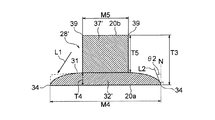
図15Aは、図14の第1金属層32’および第2金属層37’の一部を拡大して示す図である。図15Aに示すように、蒸着マスク20の第2面20bにおける第2金属層37’の幅M5は、蒸着マスク20の第1面20aにおける第1金属層32’の幅M4よりも小さくなっている。言い換えると、第2面20bにおける貫通孔25(第2開口部35)の開口寸法S2は、第1面20aにおける貫通孔25(第1開口部30)の開口寸法S1よりも大きくなっている。以下、このように第1金属層32’および第2金属層37’を構成することの利点について説明する。   FIG. 15A is an enlarged view showing a part of the first metal layer 32 ′ and the second metal layer 37 ′ of FIG. 14. As shown in FIG. 15A, the width M5 of the second metal layer 37 ′ on the second surface 20b of the vapor deposition mask 20 is smaller than the width M4 of the first metal layer 32 ′ on the first surface 20a of the vapor deposition mask 20. Yes. In other words, the opening dimension S2 of the through hole 25 (second opening 35) in the second surface 20b is larger than the opening dimension S1 of the through hole 25 (first opening 30) in the first surface 20a. Hereinafter, advantages of configuring the first metal layer 32 ′ and the second metal layer 37 ′ in this way will be described.

蒸着マスク20の第2面20b側から飛来する蒸着材料98は、貫通孔25の第2開口部35および第1開口部30を順に通って有機EL基板92に付着する。有機EL基板92のうち蒸着材料98が付着する領域は、第1面20aにおける貫通孔25の開口寸法S1や開口形状によって主に定められる。ところで、図14において第2面20b側から第1面20aへ向かう矢印L1で示すように、蒸着材料98は、るつぼ94から有機EL基板92に向けて蒸着マスク20の法線方向Nに沿って移動するだけでなく、蒸着マスク20の法線方向Nに対して大きく傾斜した方向に移動することもある。ここで、仮に第2面20bにおける貫通孔25の開口寸法S2が第1面20aにおける貫通孔25の開口寸法S1と同一であるとすると、蒸着マスク20の法線方向Nに対して大きく傾斜した方向に移動する蒸着材料98の多くは、貫通孔25を通って有機EL基板92に到達するよりも前に、貫通孔25の第2開口部35の壁面36に到達して付着してしまう。従って、蒸着材料98の利用効率を高めるためには、第2開口部35の開口寸法S2を大きくすること、すなわち第2金属層37’の幅M5を小さくすることが好ましいと言える。   The vapor deposition material 98 flying from the second surface 20 b side of the vapor deposition mask 20 adheres to the organic EL substrate 92 through the second opening 35 and the first opening 30 of the through hole 25 in order. A region of the organic EL substrate 92 to which the vapor deposition material 98 adheres is mainly determined by the opening size S1 and the opening shape of the through hole 25 in the first surface 20a. By the way, as shown by an arrow L1 from the second surface 20b side to the first surface 20a in FIG. 14, the vapor deposition material 98 is along the normal direction N of the vapor deposition mask 20 from the crucible 94 toward the organic EL substrate 92. In addition to movement, the vapor deposition mask 20 may move in a direction greatly inclined with respect to the normal direction N of the vapor deposition mask 20. Here, assuming that the opening dimension S2 of the through hole 25 in the second surface 20b is the same as the opening dimension S1 of the through hole 25 in the first surface 20a, it is greatly inclined with respect to the normal direction N of the vapor deposition mask 20. Most of the vapor deposition material 98 moving in the direction reaches the wall surface 36 of the second opening 35 of the through hole 25 and adheres before reaching the organic EL substrate 92 through the through hole 25. Therefore, in order to increase the utilization efficiency of the vapor deposition material 98, it can be said that it is preferable to increase the opening dimension S2 of the second opening 35, that is, to reduce the width M5 of the second metal layer 37 '.

図14において、第2金属層37’の端部39を通るとともに第1金属層32’の壁面31に接する直線L1が、蒸着マスク20の法線方向Nに対してなす角度が、符号θ1で表されている。斜めに移動する蒸着材料98を、第2開口部35の壁面36に到達させることなく可能な限り有機EL基板92に到達させるためには、角度θ1を大きくすることが有利となる。角度θ1を大きくする上では、第1金属層32’の幅M4に比べて第2金属層37’の幅M5を小さくすることが有効である。また図から明らかなように、角度θ1を大きくする上では、第1金属層32’の厚みT4や第2金属層37’の厚みT5を小さくすることも有効である。ここで「第1金属層32’の厚みT4」は、第1金属層32’のうち第2金属層37’に接続される部分における厚みを意味している。なお第2金属層37’の幅M5、第1金属層32’の厚みT5や第2金属層37’の厚みT5を過剰に小さくしてしまうと、蒸着マスク20の強度が低下し、このため搬送時や使用時に蒸着マスク20が破損してしまうことが考えられる。例えば、蒸着マスク20をフレーム15に張設する際に蒸着マスク20に加えられる引張り応力によって、蒸着マスク20が破損してしまうことが考えられる。これらの点を考慮すると、第1金属層32’および第2金属層37’の寸法が以下の範囲に設定されることが好ましいと言える。これによって、上述の角度θ1を例えば45°以上にすることができる。   In FIG. 14, the angle formed by the straight line L1 passing through the end 39 of the second metal layer 37 ′ and in contact with the wall surface 31 of the first metal layer 32 ′ with respect to the normal direction N of the vapor deposition mask 20 is denoted by θ1. It is represented. In order to make the vapor deposition material 98 moving obliquely reach the organic EL substrate 92 as much as possible without reaching the wall surface 36 of the second opening 35, it is advantageous to increase the angle θ1. In order to increase the angle θ1, it is effective to make the width M5 of the second metal layer 37 'smaller than the width M4 of the first metal layer 32'. As is clear from the figure, it is also effective to reduce the thickness T4 of the first metal layer 32 'and the thickness T5 of the second metal layer 37' to increase the angle θ1. Here, the “thickness T4 of the first metal layer 32 ′” means the thickness of the portion of the first metal layer 32 ′ connected to the second metal layer 37 ′. Note that if the width M5 of the second metal layer 37 ′, the thickness T5 of the first metal layer 32 ′, and the thickness T5 of the second metal layer 37 ′ are excessively reduced, the strength of the vapor deposition mask 20 is lowered. It is conceivable that the vapor deposition mask 20 is damaged during transportation or use. For example, it is conceivable that the vapor deposition mask 20 is damaged due to the tensile stress applied to the vapor deposition mask 20 when the vapor deposition mask 20 is stretched on the frame 15. Considering these points, it can be said that the dimensions of the first metal layer 32 ′ and the second metal layer 37 ′ are preferably set in the following ranges. Thereby, the above-mentioned angle θ1 can be set to 45 ° or more, for example.

・第1面20a側における第1金属層32’の幅M4:5〜25μm
・第2面20b側における第2金属層37’の幅M5:2〜20μm
・蒸着マスク20の厚みT3:1〜50μm、より好ましくは3〜30μm、さらに好ましくは3〜25μm、さらに好ましくは3〜15μm
・第1金属層32’の厚みT4:5μm以下
・第2金属層37’の厚みT5:0.1〜50μm、より好ましくは3〜30μm、さらに好ましくは3〜25μm、さらに好ましくは3〜15μm
とりわけ、蒸着マスク20の厚みT3を15μm以下とすることにより、後述する圧延材で作製された蒸着マスク20では得ることが困難な厚みで蒸着マスク20を作製することができる。この場合、シャドーの影響を低減し、蒸着材料の利用効率を向上させることが可能な蒸着マスク20を得ることができる。
-Width M4 of the first metal layer 32 ′ on the first surface 20a side: 5 to 25 μm
-Width M5 of the second metal layer 37 ′ on the second surface 20b side: 2 to 20 μm
-Thickness T3 of the evaporation mask 20: 1 to 50 [mu] m, more preferably 3 to 30 [mu] m, still more preferably 3 to 25 [mu] m, still more preferably 3 to 15 [mu] m
The thickness T4 of the first metal layer 32 ′ is 5 μm or less. The thickness T5 of the second metal layer 37 ′ is 0.1 to 50 μm, more preferably 3 to 30 μm, still more preferably 3 to 25 μm, still more preferably 3 to 15 μm.
In particular, by setting the thickness T3 of the vapor deposition mask 20 to 15 μm or less, it is possible to produce the vapor deposition mask 20 with a thickness that is difficult to obtain with the vapor deposition mask 20 produced from a rolled material described later. In this case, it is possible to obtain the vapor deposition mask 20 capable of reducing the influence of shadow and improving the utilization efficiency of the vapor deposition material.

表3に、5インチの有機EL表示装置において、表示画素数、および表示画素数に応じて求められる、蒸着マスク20の各部分の幅や厚みの値の例を示す。なお「FHD」は、Full High Definitionを意味し、「WQHD」は、Wide Quad High Definitionを意味し、「UHD」は、Ultra High Definitionを意味している。

Figure 0006443457
Table 3 shows an example of the values of the width and thickness of each part of the vapor deposition mask 20 which are obtained in accordance with the number of display pixels and the number of display pixels in the 5-inch organic EL display device. “FHD” means Full High Definition, “WQHD” means Wide Quad High Definition, and “UHD” means Ultra High Definition.
Figure 0006443457

次に、第1金属層32’の形状についてより詳細に説明する。仮に図15Aにおいて点線で示すように、端部34において第1金属層32’が、第2面20b側へ向かって大きく切り立った形状を有している場合、貫通孔25の第2開口部35を通過した後の蒸着材料98の多くが第1金属層32’の壁面31に到達して付着してしまうことが考えられる。このような、端部34近傍における第1金属層32’への蒸着材料98の付着を抑制するため、図15Aに示すように、第1金属層32’は、端部34およびその近傍において、第1金属層32’のうち第2金属層37’に接続される部分における厚みT4よりも小さな厚みを有することが好ましい。例えば図15Aに示すように、第1金属層32’の厚みが、第1金属層32’のうち第2金属層37’に接続される部分から端部34に向かうにつれて減少していることが好ましい。このような第1金属層32’の形状は、後述するように、めっき処理によって第1金属層32’を形成することによって実現され得る。   Next, the shape of the first metal layer 32 'will be described in more detail. As shown by a dotted line in FIG. 15A, when the first metal layer 32 ′ has a shape that is greatly raised toward the second surface 20 b at the end portion 34, the second opening 35 of the through hole 25. It is conceivable that much of the vapor deposition material 98 after passing through reaches the wall surface 31 of the first metal layer 32 ′ and adheres thereto. In order to suppress the adhesion of the vapor deposition material 98 to the first metal layer 32 ′ in the vicinity of the end portion 34, as shown in FIG. 15A, the first metal layer 32 ′ The first metal layer 32 ′ preferably has a thickness smaller than the thickness T4 in the portion connected to the second metal layer 37 ′. For example, as shown in FIG. 15A, the thickness of the first metal layer 32 ′ decreases from the portion of the first metal layer 32 ′ connected to the second metal layer 37 ′ toward the end 34. preferable. Such a shape of the first metal layer 32 ′ can be realized by forming the first metal layer 32 ′ by plating as described later.

図15Aにおいて、蒸着機から、第2金属層37’の端部39を通ることなく第1金属層32’の壁面31に接する直線L2が表されている。この直線L2が蒸着マスク20の法線方向Nに対してなす角度は、符号θ2となっている。この角度θ2は、端部39を通らないために上述した角度θ1よりも小さくなっている。このような角度θ2に相当する蒸着角度φ(=90°−θ2)を有する蒸着機に蒸着マスク20を適用した場合には、図15Bに示すようなシャドーが発生し得る。ここで、角度θ2について、図15Bを用いてより詳細に説明する。   In FIG. 15A, a straight line L2 coming into contact with the wall surface 31 of the first metal layer 32 'without passing through the end 39 of the second metal layer 37' is shown from the vapor deposition machine. The angle formed by the straight line L2 with respect to the normal direction N of the vapor deposition mask 20 is represented by the symbol θ2. This angle θ2 is smaller than the angle θ1 described above in order not to pass through the end 39. When the vapor deposition mask 20 is applied to a vapor deposition machine having a vapor deposition angle φ (= 90 ° −θ2) corresponding to such an angle θ2, a shadow as shown in FIG. 15B can occur. Here, the angle θ2 will be described in more detail with reference to FIG. 15B.

図15Bには、二点鎖線で示すように矩形状に形成された第1金属層32’の壁面31の角部を通る直線L3が法線方向Nに対してなす角度をθ2’とした場合に、シャドーSH1が発生し得ることが示されている。このように壁面31が矩形状に形成されている場合では、厚みを小さくすることによりシャドーを小さくすることが可能となるが、この場合には、蒸着マスク20の強度が低下し得る。   In FIG. 15B, the angle formed by the straight line L3 passing through the corner portion of the wall surface 31 of the first metal layer 32 ′ formed in a rectangular shape as indicated by a two-dot chain line with respect to the normal direction N is θ2 ′. It is shown that shadow SH1 can occur. In this way, when the wall surface 31 is formed in a rectangular shape, it is possible to reduce the shadow by reducing the thickness, but in this case, the strength of the vapor deposition mask 20 can be reduced.

これに対して、図15Bに示すように、湾曲状に形成された壁面31に接する角度θ2’の直線L4によって発生し得るシャドーは、SH2となる。このシャドーSH2は、上述のシャドーSH1よりも小さくなっている。このことにより、壁面31が矩形状に形成された場合よりも湾曲状に形成された場合の方が、シャドーを小さくすることができる。言い換えると、同じシャドーを得るためには、壁面31が矩形状に形成された場合よりも湾曲状に形成された場合の方が、当該壁面31に接する直線の角度を大きくすることができる。すなわち、図15Bに示すように、湾曲状の壁面31に接する直線L5の角度が、θ2’よりも大きいθ2’’である場合であっても、得られるシャドーはSH1となる。このことにより、壁面31が湾曲状に形成された蒸着マスク20は、角度θ2が大きくなり得る、すなわち蒸着角度φが小さくなり得る蒸着機に適用することができる。また、第1金属層32’の厚みを小さくしなくても、壁面31を湾曲状に形成することによって当該壁面31に接する直線の角度が大きくなるため、蒸着マスク20の強度を確保することもできる。   On the other hand, as shown in FIG. 15B, the shadow that can be generated by the straight line L4 of the angle θ2 ′ that contacts the curved wall surface 31 is SH2. This shadow SH2 is smaller than the above-described shadow SH1. Thereby, the shadow can be made smaller when the wall surface 31 is formed in a curved shape than when the wall surface 31 is formed in a rectangular shape. In other words, in order to obtain the same shadow, the angle of the straight line in contact with the wall surface 31 can be made larger when the wall surface 31 is formed in a curved shape than when the wall surface 31 is formed in a rectangular shape. That is, as shown in FIG. 15B, even when the angle of the straight line L5 in contact with the curved wall surface 31 is θ2 ″ larger than θ2 ′, the obtained shadow is SH1. Thereby, the vapor deposition mask 20 in which the wall surface 31 is formed in a curved shape can be applied to a vapor deposition machine in which the angle θ2 can be increased, that is, the vapor deposition angle φ can be decreased. Even if the thickness of the first metal layer 32 ′ is not reduced, by forming the wall surface 31 in a curved shape, the angle of the straight line in contact with the wall surface 31 is increased, so that the strength of the vapor deposition mask 20 can be ensured. it can.

このようにして、蒸着マスク20を、図15Aに示す角度θ2が大きくなり得る蒸着機に適用可能とすることが好適である。例えば、上述したように壁面31を湾曲状に形成することにより、角度θ2が、好ましくは30°以上、より好ましくは45°以上となり得る蒸着機に適用することが可能となる。   In this manner, it is preferable that the vapor deposition mask 20 is applicable to a vapor deposition machine that can increase the angle θ2 shown in FIG. 15A. For example, by forming the wall surface 31 in a curved shape as described above, it is possible to apply to an evaporation machine in which the angle θ2 can be preferably 30 ° or more, more preferably 45 ° or more.

このような壁面31の湾曲形状も、めっき処理によって第1金属層32’を形成することによって実現され得る。なお「壁面31」とは、第1金属層32’の面のうち第1開口部30を画成する面のことである。上述の「壁面36」も同様に、第2金属層37’の面のうち第2開口部35を画成する面のことである。   Such a curved shape of the wall surface 31 can also be realized by forming the first metal layer 32 ′ by plating. The “wall surface 31” is a surface that defines the first opening 30 in the surface of the first metal layer 32 ′. Similarly, the above-mentioned “wall surface 36” is a surface that defines the second opening 35 in the surface of the second metal layer 37 ′.

(蒸着マスクの製造方法)
次に、以上のような構成からなる蒸着マスク20を製造する方法について、図16〜図21Bを参照して説明する。
(Method for manufacturing vapor deposition mask)
Next, a method for manufacturing the vapor deposition mask 20 having the above configuration will be described with reference to FIGS.

まず、後述する基材51’上に、めっき処理によって、貫通孔25が設けられた金属層組合体28’(マスク本体)を形成する工程が実施される。当該工程は、具体的には、後述する第1成膜工程と、第2成膜工程と、を有している。   First, a step of forming a metal layer combination 28 ′ (mask main body) provided with the through holes 25 on a base material 51 ′ described later is performed by plating. Specifically, the process includes a first film forming process and a second film forming process which will be described later.

(第1成膜工程)
はじめに、絶縁性を有する基材51’上に所定のパターンで第1開口部30が設けられた第1金属層32’を形成する第1成膜工程について説明する。まず図16に示すように、絶縁性を有する基材51’と、基材51’上に形成された導電性パターン52’と、を有するパターン基板50を準備する準備工程を実施する。導電性パターン52’は、第1金属層32’に対応するパターンを有している。絶縁性および適切な強度を有する限りにおいて基材51’を構成する材料や基材51’の厚みが特に限られることはない。例えば基材51’を構成する材料として、ガラスや合成樹脂などを用いることができる。
(First film formation step)
First, the first film forming step for forming the first metal layer 32 ′ in which the first openings 30 are provided in a predetermined pattern on the insulating base material 51 ′ will be described. First, as shown in FIG. 16, a preparatory process for preparing a pattern substrate 50 having an insulating base 51 ′ and a conductive pattern 52 ′ formed on the base 51 ′ is performed. The conductive pattern 52 ′ has a pattern corresponding to the first metal layer 32 ′. As long as it has insulation and appropriate strength, the material constituting the base 51 'and the thickness of the base 51' are not particularly limited. For example, glass, synthetic resin, or the like can be used as a material constituting the substrate 51 ′.

導電性パターン52’を構成する材料としては、金属材料や酸化物導電性材料等の導電性を有する材料が適宜用いられる。金属材料の例としては、例えばクロムや銅などを挙げることができる。好ましくは、後述するレジストパターン60’に対する高い密着性を有する材料が、導電性パターン52’を構成する材料として用いられる。例えばレジストパターン60’が、アクリル系光硬化性樹脂を含むレジスト膜など、いわゆるドライフィルムと称されるものをパターニングすることによって作製される場合、導電性パターン52’を構成する材料として、ドライフィルムに対する高い密着性を有する銅が用いられることが好ましい。   As a material constituting the conductive pattern 52 ', a conductive material such as a metal material or an oxide conductive material is appropriately used. Examples of the metal material include chrome and copper. Preferably, a material having high adhesion to a resist pattern 60 'described later is used as a material constituting the conductive pattern 52'. For example, when the resist pattern 60 ′ is formed by patterning a so-called dry film such as a resist film containing an acrylic photocurable resin, a dry film is used as a material constituting the conductive pattern 52 ′. It is preferable to use copper having high adhesiveness to.

後述するように、導電性パターン52’の上には、導電性パターン52’を覆うように第1金属層32’が形成され、この第1金属層32’はその後の工程で導電性パターン52’から分離される。例えば導電性パターン52’の厚みは、50〜500nmの範囲内になっている。   As will be described later, a first metal layer 32 ′ is formed on the conductive pattern 52 ′ so as to cover the conductive pattern 52 ′, and this first metal layer 32 ′ is formed in a subsequent process by the conductive pattern 52 ′. Separated from '. For example, the thickness of the conductive pattern 52 ′ is in the range of 50 to 500 nm.

次に、導電性パターン52’が形成された基材51’上に第1めっき液を供給して、導電性パターン52’上に第1金属層32’を析出させる第1めっき処理工程を実施する。例えば、導電性パターン52’が形成された基材51’を、第1めっき液が充填されためっき槽に浸す。これによって、図17Aに示すように、パターン基板50上に、所定のパターンで第1開口部30が設けられた第1金属層32’を得ることができる。図17Bは、基材51’上に形成された第1金属層32’を示す平面図である。   Next, a first plating process is performed in which the first plating solution is supplied onto the base material 51 ′ on which the conductive pattern 52 ′ is formed to deposit the first metal layer 32 ′ on the conductive pattern 52 ′. To do. For example, the base material 51 ′ on which the conductive pattern 52 ′ is formed is immersed in a plating tank filled with the first plating solution. As a result, as shown in FIG. 17A, the first metal layer 32 ′ in which the first openings 30 are provided in a predetermined pattern can be obtained on the pattern substrate 50. FIG. 17B is a plan view showing the first metal layer 32 ′ formed on the base material 51 ′.

なおめっき処理の特性上、図17Aに示すように、第1金属層32’は、基材51’の法線方向に沿って見た場合に導電性パターン52’と重なる部分だけでなく、導電性パターン52’と重ならない部分にも形成され得る。これは、導電性パターン52’の端部53’と重なる部分に析出した第1金属層32’の表面にさらに第1金属層32’が析出するためである。この結果、図17Aに示すように、第1金属層32’の端部34は、基材51’の法線方向に沿って見た場合に導電性パターン52’と重ならない部分に位置するようになり得る。一方、金属の析出が厚み方向でなく基材51’の板面方向に進んだ分だけ、端部34およびその近傍における第1金属層32’の厚みは、中央部における厚みに比べて小さくなる。例えば図17Aに示すように、第1金属層32’の中央部から端部34に向かうにつれて第1金属層32’の厚みが少なくとも部分的に減少し、端部34およびその近傍(あるいは壁面31)が湾曲状に形成される。この結果、上述したように、適用可能な蒸着機の蒸着角度φを小さく(角度θ2を大きく)することができる。   Note that, as shown in FIG. 17A, the first metal layer 32 ′ is not only a portion overlapping the conductive pattern 52 ′ when viewed along the normal direction of the base material 51 ′, as shown in FIG. 17A. It may also be formed in a portion that does not overlap the sex pattern 52 ′. This is because the first metal layer 32 ′ is further deposited on the surface of the first metal layer 32 ′ deposited on the portion overlapping the end portion 53 ′ of the conductive pattern 52 ′. As a result, as shown in FIG. 17A, the end 34 of the first metal layer 32 ′ is positioned at a portion that does not overlap with the conductive pattern 52 ′ when viewed along the normal direction of the base 51 ′. Can be. On the other hand, the thickness of the first metal layer 32 ′ at the end portion 34 and in the vicinity thereof is smaller than the thickness at the central portion by the amount that the metal deposition has advanced in the plate surface direction of the base material 51 ′ instead of the thickness direction. . For example, as shown in FIG. 17A, the thickness of the first metal layer 32 ′ decreases at least partly from the center of the first metal layer 32 ′ toward the end 34, and the end 34 and its vicinity (or the wall surface 31). ) Is formed in a curved shape. As a result, as described above, the vapor deposition angle φ of the applicable vapor deposition machine can be reduced (the angle θ2 is increased).

図17Aにおいて、第1金属層32’のうち導電性パターン52’と重ならない部分の幅が符号wで表されている。幅wは、例えば0.5〜5.0μmの範囲内になる。導電性パターン52’の寸法は、この幅wを考慮して設定される。   In FIG. 17A, the width of the portion of the first metal layer 32 ′ that does not overlap with the conductive pattern 52 ′ is represented by the symbol w. The width w is in the range of 0.5 to 5.0 μm, for example. The dimension of the conductive pattern 52 'is set in consideration of the width w.

導電性パターン52’上に第1金属層32’を析出させることができる限りにおいて、第1めっき処理工程の具体的な方法が特に限られることはない。例えば第1めっき処理工程は、導電性パターン52’に電流を流すことによって導電性パターン52’上に第1金属層32’を析出させる、いわゆる電解めっき処理工程として実施されてもよい。若しくは、第1めっき処理工程は、無電解めっき処理工程であってもよい。なお第1めっき処理工程が無電解めっき処理工程である場合、導電性パターン52’上には適切な触媒層が設けられる。電解めっき処理工程が実施される場合にも、導電性パターン52’上に触媒層が設けられていてもよい。   As long as the first metal layer 32 ′ can be deposited on the conductive pattern 52 ′, the specific method of the first plating process is not particularly limited. For example, the first plating process may be performed as a so-called electrolytic plating process in which the first metal layer 32 ′ is deposited on the conductive pattern 52 ′ by passing a current through the conductive pattern 52 ′. Alternatively, the first plating process may be an electroless plating process. When the first plating process is an electroless plating process, an appropriate catalyst layer is provided on the conductive pattern 52 '. Even when the electrolytic plating treatment step is performed, a catalyst layer may be provided on the conductive pattern 52 ′.

用いられる第1めっき液の成分は、第1金属層32’に求められる特性に応じて適宜定められる。例えば第1金属層32’が、ニッケルを含む鉄合金によって構成される場合、第1めっき液として、ニッケル化合物を含む溶液と、鉄化合物を含む溶液との混合溶液を用いることができる。例えば、スルファミン酸ニッケルや臭化ニッケルを含む溶液と、スルファミン酸第一鉄を含む溶液との混合溶液を用いることができる。めっき液には、様々な添加剤が含まれていてもよい。添加剤としては、例えば、ホウ酸などのpH緩衝材や、マロン酸やサッカリンなどの添加剤が含まれていてもよい。   The components of the first plating solution used are appropriately determined according to the characteristics required for the first metal layer 32 '. For example, when the first metal layer 32 ′ is made of an iron alloy containing nickel, a mixed solution of a solution containing a nickel compound and a solution containing an iron compound can be used as the first plating solution. For example, a mixed solution of a solution containing nickel sulfamate or nickel bromide and a solution containing ferrous sulfamate can be used. Various additives may be contained in the plating solution. As the additive, for example, a pH buffer material such as boric acid, or an additive such as malonic acid or saccharin may be contained.

(第2成膜工程)
次に、第1開口部30に連通する第2開口部35が設けられた第2金属層37’を第1金属層32’上に形成する第2成膜工程を実施する。まず、パターン基板50の基材51’上および第1金属層32’上に、所定の隙間64’を空けてレジストパターン60’を形成するレジスト形成工程を実施する。図18Aおよび図18Bは、基材51’上に形成されたレジストパターン60’を示す断面図および平面図である。図18Aおよび図18Bに示すように、レジスト形成工程は、第1金属層32’の第1開口部30がレジストパターン60’によって覆われるとともに、レジストパターン60’の隙間64’が第1金属層32’上に位置するように実施される。
(Second film formation step)
Next, a second film forming step is performed in which a second metal layer 37 ′ having a second opening 35 communicating with the first opening 30 is formed on the first metal layer 32 ′. First, a resist formation step is performed in which a resist pattern 60 ′ is formed on the base 51 ′ and the first metal layer 32 ′ of the pattern substrate 50 with a predetermined gap 64 ′. 18A and 18B are a cross-sectional view and a plan view showing a resist pattern 60 ′ formed on a base material 51 ′. As shown in FIGS. 18A and 18B, in the resist formation step, the first opening 30 of the first metal layer 32 ′ is covered with the resist pattern 60 ′, and the gap 64 ′ of the resist pattern 60 ′ is formed in the first metal layer. It is carried out so that it may be located on 32 '.

以下、レジスト形成工程の一例について説明する。はじめに、パターン基板50の基材51’上および第1金属層32’上にドライフィルムを貼り付けることによって、ネガ型のレジスト膜を形成する。ドライフィルムの例としては、例えば日立化成製のRY3310など、アクリル系光硬化性樹脂を含むものを挙げることができる。次に、レジスト膜のうち隙間64’となるべき領域に光を透過させないようにした露光マスクを準備し、露光マスクをレジスト膜上に配置する。その後、真空密着によって露光マスクをレジスト膜に十分に密着させる。なおレジスト膜として、ポジ型のものが用いられてもよい。この場合、露光マスクとして、レジスト膜のうちの除去したい領域に光を透過させるようにした露光マスクが用いられる。   Hereinafter, an example of the resist forming process will be described. First, a negative resist film is formed by attaching a dry film on the base material 51 ′ and the first metal layer 32 ′ of the pattern substrate 50. Examples of the dry film include those containing an acrylic photocurable resin such as RY3310 manufactured by Hitachi Chemical. Next, an exposure mask is prepared so as not to transmit light to the region of the resist film where the gap 64 ′ is to be formed, and the exposure mask is disposed on the resist film. Thereafter, the exposure mask is sufficiently adhered to the resist film by vacuum adhesion. Note that a positive type resist film may be used. In this case, an exposure mask in which light is transmitted through a region to be removed of the resist film is used as the exposure mask.

その後、レジスト膜を露光マスク越しに露光する。さらに、露光されたレジスト膜に像を形成するためにレジスト膜を現像する。以上のようにして、図18Aおよび図18Bに示すように、第1金属層32’上に位置する隙間64’が設けられるとともに第1金属層32’の第1開口部30を覆うレジストパターン60’を形成することができる。なお、レジストパターン60’を基材51’および第1金属層32’に対してより強固に密着させるため、現像工程の後にレジストパターン60’を加熱する熱処理工程を実施してもよい。   Thereafter, the resist film is exposed through an exposure mask. Further, the resist film is developed to form an image on the exposed resist film. As described above, as shown in FIGS. 18A and 18B, a resist pattern 60 is provided that has a gap 64 ′ positioned on the first metal layer 32 ′ and covers the first opening 30 of the first metal layer 32 ′. 'Can be formed. Note that a heat treatment step of heating the resist pattern 60 ′ may be performed after the development step in order to make the resist pattern 60 ′ more firmly adhere to the base material 51 ′ and the first metal layer 32 ′.

次に、レジストパターン60’の隙間64’に第2めっき液を供給して、第1金属層32’上に第2金属層37’を析出させる第2めっき処理工程を実施する。例えば、第1金属層32’が形成された基材51’を、第2めっき液が充填されためっき槽に浸す。これによって、図19に示すように、第1金属層32’上に第2金属層37’を形成することができる。   Next, a second plating process is performed in which a second plating solution is supplied to the gap 64 ′ of the resist pattern 60 ′ to deposit the second metal layer 37 ′ on the first metal layer 32 ′. For example, the substrate 51 ′ on which the first metal layer 32 ′ is formed is immersed in a plating tank filled with the second plating solution. As a result, as shown in FIG. 19, the second metal layer 37 'can be formed on the first metal layer 32'.

第1金属層32’上に第2金属層37’を析出させることができる限りにおいて、第2めっき処理工程の具体的な方法が特に限られることとはない。例えば、第2めっき処理工程は、第1金属層32’に電流を流すことによって第1金属層32’上に第2金属層37’を析出させる、いわゆる電解めっき処理工程として実施されてもよい。若しくは、第2めっき処理工程は、無電解めっき処理工程であってもよい。なお第2めっき処理工程が無電解めっき処理工程である場合、第1金属層32’上には適切な触媒層が設けられる。電解めっき処理工程が実施される場合にも、第1金属層32’上に触媒層が設けられていてもよい。   As long as the second metal layer 37 ′ can be deposited on the first metal layer 32 ′, the specific method of the second plating process is not particularly limited. For example, the second plating process may be performed as a so-called electrolytic plating process in which a second metal layer 37 ′ is deposited on the first metal layer 32 ′ by passing a current through the first metal layer 32 ′. . Alternatively, the second plating process may be an electroless plating process. When the second plating process is an electroless plating process, an appropriate catalyst layer is provided on the first metal layer 32 '. Even when the electrolytic plating treatment step is performed, a catalyst layer may be provided on the first metal layer 32 ′.

第2めっき液としては、上述の第1めっき液と同一のめっき液が用いられてもよい。若しくは、第1めっき液とは異なるめっき液が第2めっき液として用いられてもよい。第1めっき液の組成と第2めっき液の組成とが同一である場合、第1金属層32’を構成する金属の組成と、第2金属層37’を構成する金属の組成も同一になる。   As the second plating solution, the same plating solution as the first plating solution described above may be used. Alternatively, a plating solution different from the first plating solution may be used as the second plating solution. When the composition of the first plating solution and the composition of the second plating solution are the same, the composition of the metal constituting the first metal layer 32 ′ and the composition of the metal constituting the second metal layer 37 ′ are also the same. .

なお図19においては、レジストパターン60’の上面と第2金属層37’の上面とが一致するようになるまで第2めっき処理工程が継続される例を示したが、これに限られることはない。第2金属層37’の上面がレジストパターン60’の上面よりも下方に位置する状態で、第2めっき処理工程が停止されてもよい。   FIG. 19 shows an example in which the second plating process is continued until the upper surface of the resist pattern 60 ′ and the upper surface of the second metal layer 37 ′ coincide with each other. However, the present invention is not limited to this. Absent. The second plating process may be stopped with the upper surface of the second metal layer 37 ′ positioned below the upper surface of the resist pattern 60 ′.

このようにして、第1金属層32’上に第2金属層37’が形成され、図14および図15Aに示す第1金属層32’と第2金属層37’とを有する金属層組合体28’が得られる。   In this way, the second metal layer 37 ′ is formed on the first metal layer 32 ′, and the metal layer combination having the first metal layer 32 ′ and the second metal layer 37 ′ shown in FIGS. 14 and 15A. 28 'is obtained.

(除去工程)
その後、図20に示すように、レジストパターン60’を除去する除去工程を実施する。例えばアルカリ系剥離液を用いることによって、レジストパターン60’を基材51’、第1金属層32’や第2金属層37’から剥離させることができる。
(Removal process)
Thereafter, as shown in FIG. 20, a removing process for removing the resist pattern 60 ′ is performed. For example, by using an alkaline stripping solution, the resist pattern 60 ′ can be stripped from the base material 51 ′, the first metal layer 32 ′, and the second metal layer 37 ′.

(分離工程)
次に、第1金属層32’および第2金属層37’を有する金属層組合体28’をパターン基板50の基材51’から分離させる分離工程を実施する。これによって、図21Aに示すように、所定のパターンで第1開口部30が設けられた第1金属層32’と、第1開口部30に連通する第2開口部35が設けられた第2金属層37’と、を備えた蒸着マスク20を得ることができる。図21Bは、蒸着マスク20を第2面20b側から見た場合を示す平面図である。
(Separation process)
Next, a separation step of separating the metal layer combination 28 ′ having the first metal layer 32 ′ and the second metal layer 37 ′ from the base material 51 ′ of the pattern substrate 50 is performed. Accordingly, as shown in FIG. 21A, the first metal layer 32 ′ provided with the first opening 30 in a predetermined pattern and the second opening 35 provided with the second opening 35 communicating with the first opening 30 are provided. The vapor deposition mask 20 provided with the metal layer 37 ′ can be obtained. FIG. 21B is a plan view illustrating the vapor deposition mask 20 as viewed from the second surface 20b side.

以下、分離工程の一例について詳細に説明する。はじめに、粘着性を有する物質が塗工などによって設けられているフィルムを、基材51’上に形成された金属層組合体28’に貼り付ける。次に、フィルムを引き上げたり巻き取ったりすることにより、フィルムを基材51’から引き離し、これによって、金属層組合体28’をパターン基板50の基材51’から分離させる。その後、金属層組合体28’からフィルムを剥がす。その他にも、分離工程においては、はじめに、金属層組合体28’と基材51’との間に、分離のきっかけとなる間隙を形成し、次に、この間隙にエアを吹き付け、これによって分離工程を促進してもよい。   Hereinafter, an example of the separation step will be described in detail. First, a film provided with an adhesive substance by coating or the like is attached to the metal layer combination 28 ′ formed on the base material 51 ′. Next, the film is pulled up or wound up to separate the film from the base material 51 ′, thereby separating the metal layer combination 28 ′ from the base material 51 ′ of the pattern substrate 50. Thereafter, the film is peeled off from the metal layer combination 28 '. In addition, in the separation step, first, a gap is formed between the metal layer combination 28 'and the base material 51' as a trigger for separation, and then air is blown into the gap, thereby separating. The process may be accelerated.

なお粘着性を有する物質としては、UVなどの光を照射されることによって、または加熱されることによって粘着性を喪失する物質を使用してもよい。この場合、金属層組合体28’を基材51’から分離させた後、フィルムに光を照射する工程やフィルムを加熱する工程を実施する。これによって、金属層組合体28’からフィルムを剥がす工程を容易化することができる。例えば、フィルムと金属層組合体28’とを可能な限り互いに平行な状態に維持した状態で、フィルムを剥がすことができる。これによって、フィルムを剥がす際に金属層組合体28’が湾曲することを抑制することができ、このことにより、蒸着マスク20に湾曲などの変形のくせがついてしまうことを抑制することができる。   Note that as the substance having adhesiveness, a substance that loses adhesiveness when irradiated with light such as UV or when heated may be used. In this case, after separating the metal layer combination 28 ′ from the base material 51 ′, a step of irradiating the film with light and a step of heating the film are performed. This can facilitate the process of peeling the film from the metal layer combination 28 '. For example, the film can be peeled off while keeping the film and the metal layer combination 28 'as parallel as possible. Accordingly, it is possible to suppress the metal layer combination 28 ′ from being bent when the film is peeled off, and thus it is possible to suppress the deposition mask 20 from being deformed such as a curve.

上述した形態2によれば、上述のように、レジストパターン60’の隙間64’に第2めっき液を供給して、第1金属層32’上に第2金属層37’を析出させることによって、蒸着マスク20が作製される。このため、蒸着マスク20の貫通孔25に、第1金属層32’の第1開口部30によって画定される形状、および、第2金属層37’の第2開口部35によって画定される形状の両方を付与することができる。従って、複雑な形状を有する貫通孔25を精密に形成することができる。例えば、上述の角度θ1を大きくすることが可能な貫通孔25を得ることができる。とりわけ、第1金属層32’の端部34およびその近傍を、後述する形態3よりも大きく湾曲状に形成することができるため、当該角度θ1をより一層大きくすることができる。これによって、蒸着材料98の利用効率を高めることができる。言い換えると、端部34およびその近傍が湾曲状に形成されていることにより、所定の角度θ1に対して第1金属層32’の厚みを、湾曲の度合いが小さい場合よりも大きくすることができ、第1金属層32’の強度、例えば超音波洗浄時に対する強度を増大させることができる。また、めっき処理を利用して第2金属層37’を形成することにより、貫通孔25の形状とは独立に、蒸着マスク20の厚みT3を任意に設定することができる。このため、十分な強度を蒸着マスク20に持たせることができる。従って、高精細な有機EL表示装置を製造することができ、かつ耐久性に優れた蒸着マスク20を提供することができる。さらに、上述したように、第1金属層32’の端部34およびその近傍を湾曲状に形成しているため、蒸着マスク20を適用可能な蒸着機の蒸着角度φを小さく(角度θ2を大きく)することができる。   According to the above-described form 2, as described above, the second plating solution is supplied to the gap 64 ′ of the resist pattern 60 ′ to deposit the second metal layer 37 ′ on the first metal layer 32 ′. The vapor deposition mask 20 is produced. Therefore, the shape defined by the first opening 30 of the first metal layer 32 ′ and the shape defined by the second opening 35 of the second metal layer 37 ′ are formed in the through hole 25 of the vapor deposition mask 20. Both can be granted. Therefore, the through hole 25 having a complicated shape can be precisely formed. For example, the through hole 25 capable of increasing the above-described angle θ1 can be obtained. In particular, the end portion 34 of the first metal layer 32 ′ and the vicinity thereof can be formed in a curved shape that is larger than that of the third embodiment to be described later, so that the angle θ 1 can be further increased. Thereby, the utilization efficiency of the vapor deposition material 98 can be improved. In other words, since the end portion 34 and the vicinity thereof are formed in a curved shape, the thickness of the first metal layer 32 ′ can be increased with respect to the predetermined angle θ1 as compared with the case where the degree of bending is small. The strength of the first metal layer 32 ′, for example, the strength with respect to ultrasonic cleaning can be increased. Further, by forming the second metal layer 37 ′ using a plating process, the thickness T <b> 3 of the vapor deposition mask 20 can be arbitrarily set independently of the shape of the through hole 25. For this reason, the vapor deposition mask 20 can have sufficient strength. Therefore, a high-definition organic EL display device can be manufactured, and the vapor deposition mask 20 excellent in durability can be provided. Furthermore, as described above, since the end portion 34 of the first metal layer 32 ′ and the vicinity thereof are formed in a curved shape, the vapor deposition angle φ of the vapor deposition machine to which the vapor deposition mask 20 can be applied is reduced (the angle θ2 is increased). )can do.

〔形態3 2層構造を有する蒸着マスクのめっき処理による製造方法の他の例〕
次に、2層構造を有する蒸着マスクのめっき処理による製造方法の他の例について説明する。当該製造方法により製造される蒸着マスク20の構造は、図14に示す形態2の構造と略同一となるため、ここでは詳細な説明は省略する。以下に、形態3における蒸着マスク20を製造する方法について、図22〜図28を参照して説明する。
[Form 3 Another Example of Manufacturing Method by Plating of Evaporation Mask Having Two-Layer Structure]
Next, another example of the manufacturing method by plating of the vapor deposition mask having a two-layer structure will be described. Since the structure of the vapor deposition mask 20 manufactured by the manufacturing method is substantially the same as that of the second embodiment shown in FIG. 14, detailed description thereof is omitted here. Below, the method to manufacture the vapor deposition mask 20 in the form 3 is demonstrated with reference to FIGS.

まず、後述する基材51’’上に、めっき処理によって、貫通孔25が設けられた金属層組合体28’(マスク本体)を形成する工程が実施される。当該工程は、具体的には、後述する第1成膜工程と、第2成膜工程と、を有している。   First, a step of forming a metal layer combination 28 ′ (mask body) provided with the through holes 25 on a base material 51 ″ described later is performed by plating. Specifically, the process includes a first film forming process and a second film forming process which will be described later.

(第1成膜工程)
はじめに図22に示すように、めっき処理の際の下地となる基材51’’を準備する準備工程を実施する。ここでは、めっき処理が電解めっき処理である例について説明する。この場合、基材51’’の表面51a’’のうち少なくとも第1金属層32’が析出する部分は、導電性を有する導電層によって構成されている。例えば、基材51’’全体が、導電性を有する導電層によって構成されていてもよい。この場合、基材51’’のうち表面51a’’の反対側に位置する裏面51b’’には、裏面51b’’が他の部材と導通してしまうことを防ぐための、絶縁性を有するカバーフィルム52’’が設けられていてもよい。
(First film formation step)
First, as shown in FIG. 22, a preparatory step for preparing a base material 51 ″ as a base in the plating process is performed. Here, an example in which the plating process is an electrolytic plating process will be described. In this case, at least a portion of the surface 51a ″ of the base 51 ″ where the first metal layer 32 ′ is deposited is constituted by a conductive layer having conductivity. For example, the whole substrate 51 ″ may be constituted by a conductive layer having conductivity. In this case, the back surface 51b '' located on the opposite side of the front surface 51a '' of the base material 51 '' has an insulating property to prevent the back surface 51b '' from conducting with other members. A cover film 52 '' may be provided.

後述するめっき処理の際に所定の金属を析出させることができる限りにおいて、基材51’’の導電層を構成する材料が特に限られることはない。例えば、基材51’’の導電層を構成する材料としては、金属材料や酸化物導電性材料等の導電性を有する材料が適宜用いられる。金属材料の例としては、例えばステンレススチールや銅などを挙げることができる。好ましくは、後述する第1レジストパターン60Aに対する高い密着性を有する材料が、基材51’’の導電層を構成する材料として用いられる。例えば第1レジストパターン60Aが、アクリル系光硬化性樹脂を含むレジスト膜など、いわゆるドライフィルムと称されるものをパターニングすることによって作製される場合、基材51’’の導電層を構成する材料として、ドライフィルムに対する高い密着性を有する銅が用いられることが好ましい。   As long as a predetermined metal can be deposited during the plating process described later, the material constituting the conductive layer of the substrate 51 ″ is not particularly limited. For example, as a material forming the conductive layer of the base member 51 ″, a conductive material such as a metal material or an oxide conductive material is appropriately used. Examples of the metal material include stainless steel and copper. Preferably, a material having high adhesion to the first resist pattern 60A described later is used as a material constituting the conductive layer of the base member 51 ''. For example, when the first resist pattern 60A is formed by patterning a so-called dry film such as a resist film containing an acrylic photocurable resin, a material constituting the conductive layer of the substrate 51 ″ As such, copper having high adhesion to a dry film is preferably used.

次に、基材51’’の表面51a’’上に、所定の第1隙間64Aを空けて第1レジストパターン60Aを形成する第1レジスト形成工程を実施する。図23は、第1レジストパターン60Aが形成された基材51’’を示す断面図である。図23に示すように、第1レジストパターン60Aは、第1隙間64Aに面する側面63Aを含んでいる。   Next, a first resist formation step is performed in which a first resist pattern 60A is formed on the surface 51a '' of the base member 51 '' with a predetermined first gap 64A. FIG. 23 is a cross-sectional view showing the base material 51 ″ on which the first resist pattern 60A is formed. As shown in FIG. 23, the first resist pattern 60A includes a side surface 63A that faces the first gap 64A.

第1レジスト形成工程においては、はじめに、基材51’’の表面51a’’にドライフィルムを貼り付けることによって、ネガ型のレジスト膜を形成する。ドライフィルムの例としては、例えば日立化成製のRY3310など、アクリル系光硬化性樹脂を含むものを挙げることができる。次に、レジスト膜のうち第1隙間64Aとなるべき領域に光を透過させないようにした露光マスクを準備し、露光マスクをレジスト膜上に配置する。その後、真空密着によって露光マスクをレジスト膜に十分に密着させる。なおレジスト膜として、ポジ型のものが用いられてもよい。この場合、露光マスクとして、レジスト膜のうちの除去したい領域に光を透過させるようにした露光マスクが用いられる。   In the first resist formation step, first, a negative resist film is formed by attaching a dry film to the surface 51 a ″ of the substrate 51 ″. Examples of the dry film include those containing an acrylic photocurable resin such as RY3310 manufactured by Hitachi Chemical. Next, an exposure mask is prepared so as not to transmit light to the region of the resist film that should become the first gap 64A, and the exposure mask is disposed on the resist film. Thereafter, the exposure mask is sufficiently adhered to the resist film by vacuum adhesion. Note that a positive type resist film may be used. In this case, an exposure mask in which light is transmitted through a region to be removed of the resist film is used as the exposure mask.

その後、レジスト膜を露光マスク越しに露光する。さらに、露光されたレジスト膜に像を形成するためにレジスト膜を現像する。以上のようにして、図23に示す第1レジストパターン60Aを形成することができる。なお、第1レジストパターン60Aを基材51’’の表面51a’’に対してより強固に密着させるため、現像工程の後に第1レジストパターン60Aを加熱する熱処理工程を実施してもよい。   Thereafter, the resist film is exposed through an exposure mask. Further, the resist film is developed to form an image on the exposed resist film. As described above, the first resist pattern 60A shown in FIG. 23 can be formed. Note that a heat treatment step of heating the first resist pattern 60A may be performed after the development step in order to make the first resist pattern 60A more firmly adhere to the surface 51a '' of the substrate 51 ''.

次に、第1レジストパターン60Aが形成された基材51’’上に第1めっき液を供給して、第1隙間64Aにおける基材51’’上に第1金属層32’を析出させる第1めっき処理工程を実施する。例えば、第1レジストパターン60Aが形成された基材51’’を、第1めっき液が充填されためっき槽に浸す。これによって、図24に示すように、基材51’’上に、所定のパターンで第1開口部30が設けられた第1金属層32’を得ることができる。   Next, a first plating solution is supplied onto the substrate 51 ″ on which the first resist pattern 60A is formed, so that the first metal layer 32 ′ is deposited on the substrate 51 ″ in the first gap 64A. 1 Plating process is performed. For example, the substrate 51 ″ on which the first resist pattern 60 </ b> A is formed is immersed in a plating tank filled with the first plating solution. As a result, as shown in FIG. 24, the first metal layer 32 ′ in which the first openings 30 are provided in a predetermined pattern on the base material 51 ″ can be obtained.

なおめっき処理の特性上、図24に示すように、第1金属層32’は、基材51’’の法線方向に析出して成長していく。しかしながら、第1レジストパターン60Aの第1隙間64Aに面する側面63A付近では、第1レジストパターン60Aの存在により、第1めっき液が入り込みにくくなっていることから、金属材料の析出速度が低下する。このことにより、第1金属層32’の端部34およびその近傍は、図14および図15Aに示すような湾曲状に形成され得る。なお、図24〜図28においては、図面を明瞭化するために、端部34およびその近傍は矩形状に示されている。   Due to the characteristics of the plating process, as shown in FIG. 24, the first metal layer 32 ′ is deposited and grows in the normal direction of the base material 51 ″. However, in the vicinity of the side surface 63A facing the first gap 64A of the first resist pattern 60A, the presence of the first resist pattern 60A makes it difficult for the first plating solution to enter, so the deposition rate of the metal material decreases. . Accordingly, the end portion 34 of the first metal layer 32 ′ and the vicinity thereof can be formed in a curved shape as shown in FIGS. 14 and 15A. 24 to 28, the end 34 and the vicinity thereof are shown in a rectangular shape for the sake of clarity.

基材51’’上に第1金属層32’を析出させることができる限りにおいて、第1めっき処理工程の具体的な方法が特に限られることはない。例えば第1めっき処理工程は、基材51’’に電流を流すことによって基材51’’上に第1金属層32’を析出させる、いわゆる電解めっき処理工程として実施されてもよい。若しくは、第1めっき処理工程は、無電解めっき処理工程であってもよい。なお第1めっき処理工程が無電解めっき処理工程である場合、基材51’’上には適切な触媒層が設けられる。電解めっき処理工程が実施される場合にも、基材51’’上に触媒層が設けられていてもよい。   As long as the first metal layer 32 ′ can be deposited on the substrate 51 ″, the specific method of the first plating process is not particularly limited. For example, the first plating process may be performed as a so-called electrolytic plating process in which the first metal layer 32 ′ is deposited on the substrate 51 ″ by passing an electric current through the substrate 51 ″. Alternatively, the first plating process may be an electroless plating process. When the first plating process is an electroless plating process, an appropriate catalyst layer is provided on the substrate 51 ″. Even when the electrolytic plating treatment step is performed, a catalyst layer may be provided on the substrate 51 ″.

第1めっき液の成分は、形態2で説明した第1めっき液と同様とすることができるため、ここでは詳細な説明は省略する。   Since the components of the first plating solution can be the same as those of the first plating solution described in Embodiment 2, detailed description thereof is omitted here.

(第2成膜工程)
次に、第1開口部30に連通する第2開口部35が設けられた第2金属層37’を第1金属層32’上に形成する第2成膜工程を実施する。まず、第1レジストパターン60A上および第1金属層32’上に、所定の第2隙間64Bを空けて第2レジストパターン60Bを形成する第2レジスト形成工程を実施する。図25は、第1レジストパターン60Aおよび第1金属層32’上に形成された第2レジストパターン60Bを示す断面図である。図25に示すように、第2レジスト形成工程は、第1金属層32’の第1開口部30が第2レジストパターン60Bによって覆われるとともに、第2レジストパターン60Bの第2隙間64Bが第1金属層32’上に位置するように実施される。
(Second film formation step)
Next, a second film forming step is performed in which a second metal layer 37 ′ having a second opening 35 communicating with the first opening 30 is formed on the first metal layer 32 ′. First, a second resist forming step is performed in which a second resist pattern 60B is formed on the first resist pattern 60A and the first metal layer 32 ′ with a predetermined second gap 64B. FIG. 25 is a cross-sectional view showing the second resist pattern 60B formed on the first resist pattern 60A and the first metal layer 32 ′. As shown in FIG. 25, in the second resist forming step, the first opening 30 of the first metal layer 32 ′ is covered with the second resist pattern 60B, and the second gap 64B of the second resist pattern 60B is the first. It is carried out so as to be located on the metal layer 32 '.

第2レジストパターン60Bの形成工程は、上述した第1レジストパターン60Aの形成工程と同様に実施することができるため、ここでは詳細な説明は省略する。   Since the formation process of the 2nd resist pattern 60B can be implemented similarly to the formation process of the 1st resist pattern 60A mentioned above, detailed explanation is omitted here.

次に、第2レジストパターン60Bの第2隙間64Bに第2めっき液を供給して、第1金属層32’上に第2金属層37’を析出させる第2めっき処理工程を実施する。例えば、第1金属層32’が形成された基材51’’を、第2めっき液が充填されためっき槽に浸す。これによって、図26に示すように、第1金属層32’上に第2金属層37’を形成することができる。   Next, a second plating process is performed in which the second plating solution is supplied to the second gap 64B of the second resist pattern 60B to deposit the second metal layer 37 'on the first metal layer 32'. For example, the substrate 51 ″ on which the first metal layer 32 ′ is formed is immersed in a plating tank filled with the second plating solution. Accordingly, as shown in FIG. 26, the second metal layer 37 'can be formed on the first metal layer 32'.

第1金属層32’上に第2金属層37’を析出させることができる限りにおいて、第2めっき処理工程の具体的な方法が特に限られることとはない。例えば、第2めっき処理工程は、第1金属層32’に電流を流すことによって第1金属層32’上に第2金属層37’を析出させる、いわゆる電解めっき処理工程として実施されてもよい。若しくは、第2めっき処理工程は、無電解めっき処理工程であってもよい。なお第2めっき処理工程が無電解めっき処理工程である場合、第1金属層32’上には適切な触媒層が設けられる。電解めっき処理工程が実施される場合にも、第1金属層32’上に触媒層が設けられていてもよい。   As long as the second metal layer 37 ′ can be deposited on the first metal layer 32 ′, the specific method of the second plating process is not particularly limited. For example, the second plating process may be performed as a so-called electrolytic plating process in which a second metal layer 37 ′ is deposited on the first metal layer 32 ′ by passing a current through the first metal layer 32 ′. . Alternatively, the second plating process may be an electroless plating process. When the second plating process is an electroless plating process, an appropriate catalyst layer is provided on the first metal layer 32 '. Even when the electrolytic plating treatment step is performed, a catalyst layer may be provided on the first metal layer 32 ′.

第2めっき液としては、上述の第1めっき液と同一のめっき液が用いられてもよい。若しくは、第1めっき液とは異なるめっき液が第2めっき液として用いられてもよい。第1めっき液の組成と第2めっき液の組成とが同一である場合、第1金属層32’を構成する金属の組成と、第2金属層37’を構成する金属の組成も同一になる。   As the second plating solution, the same plating solution as the first plating solution described above may be used. Alternatively, a plating solution different from the first plating solution may be used as the second plating solution. When the composition of the first plating solution and the composition of the second plating solution are the same, the composition of the metal constituting the first metal layer 32 ′ and the composition of the metal constituting the second metal layer 37 ′ are also the same. .

なお図26においては、第2レジストパターン60Bの上面と第2金属層37’の上面とが一致するようになるまで第2めっき処理工程が継続される例を示したが、これに限られることはない。第2金属層37’の上面が第2レジストパターン60Bの上面よりも下方に位置する状態で、第2めっき処理工程が停止されてもよい。   In FIG. 26, the example in which the second plating process is continued until the upper surface of the second resist pattern 60B coincides with the upper surface of the second metal layer 37 ′ is shown. However, the present invention is not limited to this. There is no. The second plating process may be stopped with the upper surface of the second metal layer 37 ′ positioned below the upper surface of the second resist pattern 60 </ b> B.

このようにして、第1金属層32’上に第2金属層37’が形成され、図14および図15Aに示す第1金属層32’と第2金属層37’とを有する金属層組合体28’が得られる。   In this way, the second metal layer 37 ′ is formed on the first metal layer 32 ′, and the metal layer combination having the first metal layer 32 ′ and the second metal layer 37 ′ shown in FIGS. 14 and 15A. 28 'is obtained.

(除去工程)
その後、図27に示すように、第1レジストパターン60Aおよび第2レジストパターン60Bを除去する除去工程を実施する。例えばアルカリ系剥離液を用いることによって、第1レジストパターン60Aおよび第2レジストパターン60Bを基材51’’、第1金属層32’や第2金属層37’から剥離させることができる。
(Removal process)
Thereafter, as shown in FIG. 27, a removal step of removing the first resist pattern 60A and the second resist pattern 60B is performed. For example, by using an alkaline stripping solution, the first resist pattern 60A and the second resist pattern 60B can be stripped from the substrate 51 ″, the first metal layer 32 ′, and the second metal layer 37 ′.

(分離工程)
次に、第1金属層32’および第2金属層37’を有する金属層組合体28’を基材51’’から分離させる分離工程を実施する。これによって、図28に示すように、所定のパターンで第1開口部30が設けられた第1金属層32’と、第1開口部30に連通する第2開口部35が設けられた第2金属層37’と、を備えた蒸着マスク20を得ることができる。分離工程は、上述した形態2における分離工程と同様に実施することができる。
(Separation process)
Next, a separation step of separating the metal layer combination 28 ′ having the first metal layer 32 ′ and the second metal layer 37 ′ from the base material 51 ″ is performed. Thus, as shown in FIG. 28, the first metal layer 32 ′ provided with the first opening 30 in a predetermined pattern and the second opening 35 provided with the second opening 35 communicating with the first opening 30 are provided. The vapor deposition mask 20 provided with the metal layer 37 ′ can be obtained. The separation step can be performed in the same manner as the separation step in the above-described form 2.

上述した形態3によれば、上述のように、第1レジストパターン60Aの第1隙間64Aに第1めっき液を供給して第1金属層32’を析出させ、第2レジストパターン60Bの第2隙間64Bに第2めっき液を供給して、第1金属層32’上に第2金属層37’を析出させることによって、蒸着マスク20が作製される。このため、蒸着マスク20の貫通孔25に、第1金属層32’の第1開口部30によって画定される形状、および、第2金属層37’の第2開口部35によって画定される形状の両方を付与することができる。従って、複雑な形状を有する貫通孔25を精密に形成することができる。例えば、上述の角度θ1を大きくすることが可能な貫通孔25を得ることができる。これによって、蒸着材料98の利用効率を高めることができる。また、めっき処理を利用して第2金属層37’を形成することにより、貫通孔25の形状とは独立に、蒸着マスク20の厚みT3を任意に設定することができる。このため、十分な強度を蒸着マスク20に持たせることができる。従って、高精細な有機EL表示装置を製造することができ、かつ耐久性に優れた蒸着マスク20を提供することができる。   According to the above-described embodiment 3, as described above, the first plating solution is supplied to the first gap 64A of the first resist pattern 60A to deposit the first metal layer 32 ′, and the second resist pattern 60B is second. The vapor deposition mask 20 is produced by supplying the second plating solution to the gap 64B and depositing the second metal layer 37 ′ on the first metal layer 32 ′. Therefore, the shape defined by the first opening 30 of the first metal layer 32 ′ and the shape defined by the second opening 35 of the second metal layer 37 ′ are formed in the through hole 25 of the vapor deposition mask 20. Both can be granted. Therefore, the through hole 25 having a complicated shape can be precisely formed. For example, the through hole 25 capable of increasing the above-described angle θ1 can be obtained. Thereby, the utilization efficiency of the vapor deposition material 98 can be improved. Further, by forming the second metal layer 37 ′ using a plating process, the thickness T <b> 3 of the vapor deposition mask 20 can be arbitrarily set independently of the shape of the through hole 25. For this reason, the vapor deposition mask 20 can have sufficient strength. Therefore, a high-definition organic EL display device can be manufactured, and the vapor deposition mask 20 excellent in durability can be provided.

〔形態4 エッチングによって作製された蒸着マスク〕
上述の図3〜図28に示す例においては、めっき処理によって蒸着マスク20を作製する場合について説明した。しかしながら、蒸着マスク20を作製するために採用される方法が、めっき処理に限られることはない。以下、エッチングによって金属板21に貫通孔25を形成することによって蒸着マスク20を作製する例について説明する。ここで、金属板21は、エッチングによって、有機EL基板92に蒸着材料98を蒸着させる蒸着マスク20であって、複数の貫通孔25が形成された蒸着マスク20を作製するために用いられる板材である。
[Form 4 Evaporation Mask Prepared by Etching]
In the example shown in FIGS. 3 to 28 described above, the case where the vapor deposition mask 20 is produced by plating processing has been described. However, the method adopted for producing the vapor deposition mask 20 is not limited to the plating process. Hereinafter, an example in which the vapor deposition mask 20 is produced by forming the through holes 25 in the metal plate 21 by etching will be described. Here, the metal plate 21 is a vapor deposition mask 20 for depositing a vapor deposition material 98 on the organic EL substrate 92 by etching, and is a plate material used for producing the vapor deposition mask 20 in which a plurality of through holes 25 are formed. is there.

すなわち、この形態4における蒸着マスク20は、図29に示すように、金属板21(マスク本体)と、金属板21に設けられた複数の上述の貫通孔25と、を備えている。   That is, the vapor deposition mask 20 in this embodiment 4 includes a metal plate 21 (mask body) and a plurality of the above-described through holes 25 provided in the metal plate 21 as shown in FIG.

このうち金属板21は、上述した金属層28と同様に、上記式(1)を満たしている。   Among these, the metal plate 21 satisfies the above-described formula (1), similarly to the metal layer 28 described above.

ここで、本明細書では、金属板21との用語は、上述した金属層28と同様に、貫通孔25が形成されていない状態(単なる板状)の部材の概念を意味するものとして用いる。すなわち、本明細書では、概念的には、金属板21に、金属板21とは別の概念である複数の貫通孔25が設けられた構成を、蒸着マスク20が有しているとする。このことにより、金属板21が上記式(1)を満たしているとは、貫通孔25が形成されていない状態の金属板21が上記式(1)を満たしていることを意味し、貫通孔25が形成された状態の金属板21が上記式(1)を満たしていることを意味するものではない。貫通孔25が形成された状態の金属板21では、インデンテーション弾性率や0.2%耐力(若しくは、インデンテーション硬度)が、貫通孔25の大きさ、ピッチ、形状等によって影響を受けると考えられる。このため、蒸着マスク20の完成形として、金属板21に複数の貫通孔25が形成された状態においては、上記式(1)を満たす金属板21の領域は、貫通孔25が形成されていない領域、より詳細にはインデンテーション弾性率および0.2%耐力(若しくは、インデンテーション硬度)に貫通孔25の影響が及ばない領域であり、例えば、上述した周囲領域23のうち貫通孔25の影響が及ばない領域や、有効領域22のうち互いに隣り合う貫通孔25同士の間の領域となる。従って、蒸着マスク20の完成形から金属板21のインデンテーション弾性率および0.2%耐力(若しくは、インデンテーション硬度)を調べる場合には、周囲領域23のうち貫通孔25が含まれない領域を切り取って、後述するナノ・インデンテーション試験、および0.2%耐力を調べる場合には引張試験を行うことが好適である。また、有効領域22であっても、互いに隣り合う貫通孔25同士の間の距離が、ナノ・インデンテーション試験、および0.2%耐力を調べる場合の引張試験を行うことが可能な程度の距離であれば、貫通孔25同士の間の領域を切り取ってもよい。なお、材料特性の点で述べると、一般的に蒸着マスク20の金属板21は、材料の組成や材質が位置によって異なることはない。このため、貫通孔25に近い位置と、貫通孔25から離れた位置とで、材料の特性が異なることはない。   Here, in the present specification, the term “metal plate 21” is used to mean the concept of a member in which the through-hole 25 is not formed (simple plate shape), like the metal layer 28 described above. That is, in this specification, it is assumed that the vapor deposition mask 20 has a configuration in which the metal plate 21 is conceptually provided with a plurality of through holes 25 that are different from the metal plate 21. Thus, the fact that the metal plate 21 satisfies the above formula (1) means that the metal plate 21 in a state where the through hole 25 is not formed satisfies the above formula (1). It does not mean that the metal plate 21 in a state where 25 is formed satisfies the above formula (1). In the metal plate 21 in which the through holes 25 are formed, the indentation elastic modulus and 0.2% proof stress (or indentation hardness) are considered to be affected by the size, pitch, shape, etc. of the through holes 25. It is done. For this reason, in a state where a plurality of through holes 25 are formed in the metal plate 21 as a completed form of the vapor deposition mask 20, the through holes 25 are not formed in the region of the metal plate 21 that satisfies the above formula (1). The region, more specifically, the region where the through hole 25 does not affect the indentation elastic modulus and 0.2% proof stress (or indentation hardness). For example, the influence of the through hole 25 in the surrounding region 23 described above. Is an area between the through holes 25 adjacent to each other in the effective area 22. Therefore, when examining the indentation elastic modulus and 0.2% yield strength (or indentation hardness) of the metal plate 21 from the completed form of the vapor deposition mask 20, the region of the surrounding region 23 that does not include the through hole 25 is selected. It is preferable to perform a tensile test when cutting and examining the nano-indentation test described later and the 0.2% proof stress. Further, even in the effective region 22, the distance between the adjacent through holes 25 is such that the nano-indentation test and the tensile test for examining 0.2% proof stress can be performed. If so, the region between the through holes 25 may be cut off. In terms of material properties, the metal plate 21 of the vapor deposition mask 20 generally does not vary in composition and material depending on the position. For this reason, the characteristics of the material do not differ between a position close to the through hole 25 and a position away from the through hole 25.

図29は、エッチングを利用することによって作製された蒸着マスク20を、図3のA−A線に沿って切断した場合を示す断面図である。図29に示す例では、後に詳述するように、蒸着マスクの法線方向における一方の側となる金属板21の第1面21aに第1開口部30がエッチングによって形成され、金属板21の法線方向における他方の側となる第2面21bに第2開口部35がエッチングによって形成される。第1開口部30は、第2開口部35に接続され、これによって第2開口部35と第1開口部30とが互いに連通するように形成される。貫通孔25は、第2開口部35と、第2開口部35に接続された第1開口部30とによって構成されている。   FIG. 29 is a cross-sectional view showing a case where the vapor deposition mask 20 produced by using etching is cut along the line AA in FIG. In the example shown in FIG. 29, as will be described in detail later, a first opening 30 is formed by etching on the first surface 21a of the metal plate 21 on one side in the normal direction of the vapor deposition mask. A second opening 35 is formed by etching on the second surface 21b on the other side in the normal direction. The first opening portion 30 is connected to the second opening portion 35 so that the second opening portion 35 and the first opening portion 30 communicate with each other. The through hole 25 includes a second opening 35 and a first opening 30 connected to the second opening 35.

図29に示すように、蒸着マスク20の第1面20aの側から第2面20bの側へ向けて、蒸着マスク20の法線方向に沿った各位置における蒸着マスク20の板面に沿った断面での各第1開口部30の断面積は、しだいに小さくなっていく。同様に、蒸着マスク20の法線方向に沿った各位置における蒸着マスク20の板面に沿った断面での各第2開口部35の断面積は、蒸着マスク20の第2面20bの側から第1面20aの側へ向けて、しだいに小さくなっていく。   As shown in FIG. 29, along the plate surface of the vapor deposition mask 20 at each position along the normal direction of the vapor deposition mask 20 from the first surface 20 a side to the second surface 20 b side of the vapor deposition mask 20. The cross-sectional area of each first opening 30 in the cross section gradually decreases. Similarly, the cross-sectional area of each second opening 35 in the cross section along the plate surface of the vapor deposition mask 20 at each position along the normal direction of the vapor deposition mask 20 is from the second surface 20b side of the vapor deposition mask 20. It gradually becomes smaller toward the first surface 20a.

図29に示すように、第1開口部30の壁面31と、第2開口部35の壁面36とは、周状の接続部41を介して接続されている。接続部41は、蒸着マスクの法線方向に対して傾斜した第1開口部30の壁面31と、蒸着マスクの法線方向に対して傾斜した第2開口部35の壁面36とが合流する張り出し部の稜線によって、画成されている。そして、接続部41は、蒸着マスク20の平面視において貫通孔25の面積が最小になる貫通部42を画成する。   As shown in FIG. 29, the wall surface 31 of the first opening 30 and the wall surface 36 of the second opening 35 are connected via a circumferential connection portion 41. The connecting portion 41 is an overhang where the wall surface 31 of the first opening 30 inclined with respect to the normal direction of the vapor deposition mask and the wall surface 36 of the second opening 35 inclined with respect to the normal direction of the vapor deposition mask merge. It is defined by the ridgeline of the part. And the connection part 41 defines the penetration part 42 in which the area of the through-hole 25 becomes the minimum in the planar view of the vapor deposition mask 20.

図29に示すように、蒸着マスクの法線方向に沿った一方の側の面、すなわち、蒸着マスク20の第1面20a上において、隣り合う二つの貫通孔25は、蒸着マスクの板面に沿って互いから離間している。すなわち、後述する製造方法のように、蒸着マスク20の第1面20aに対応するようになる金属板21の第1面21a側から当該金属板21をエッチングして第1開口部30を作製する場合、隣り合う二つの第1開口部30の間に金属板21の第1面21aが残存するようになる。   As shown in FIG. 29, on one surface along the normal direction of the vapor deposition mask, that is, on the first surface 20a of the vapor deposition mask 20, two adjacent through holes 25 are formed on the plate surface of the vapor deposition mask. Are spaced apart from each other. That is, like the manufacturing method described later, the metal plate 21 is etched from the side of the first surface 21 a of the metal plate 21 that corresponds to the first surface 20 a of the vapor deposition mask 20 to produce the first opening 30. In this case, the first surface 21 a of the metal plate 21 remains between two adjacent first openings 30.

同様に、図29に示すように、蒸着マスクの法線方向に沿った他方の側、すなわち、蒸着マスク20の第2面20bの側においても、隣り合う二つの第2開口部35が、蒸着マスクの板面に沿って互いから離間していてもよい。すなわち、隣り合う二つの第2開口部35の間に金属板21の第2面21bが残存していてもよい。以下の説明において、金属板21の第2面21bの有効領域22のうちエッチングされずに残っている部分のことを、トップ部43とも称する。このようなトップ部43が残るように蒸着マスク20を作製することにより、蒸着マスク20に十分な強度を持たせることができる。このことにより、例えば搬送中などに蒸着マスク20が破損してしまうことを抑制することができる。なおトップ部43の幅βが大きすぎると、蒸着工程においてシャドーが発生し、これによって蒸着材料98の利用効率が低下することがある。従って、トップ部43の幅βが過剰に大きくならないように蒸着マスク20が作製されることが好ましい。例えば、トップ部43の幅βが2μm以下であることが好ましい。なおトップ部43の幅βは一般に、蒸着マスク20を切断する方向に応じて変化する。例えば、図29に示すトップ部43の幅βは互いに異なることがある。この場合、いずれの方向で蒸着マスク20を切断した場合にもトップ部43の幅βが2μm以下になるよう、蒸着マスク20が構成されていてもよい。   Similarly, as shown in FIG. 29, two adjacent second openings 35 are formed on the other side along the normal direction of the vapor deposition mask, that is, on the second surface 20 b side of the vapor deposition mask 20. They may be spaced apart from each other along the plate surface of the mask. That is, the second surface 21b of the metal plate 21 may remain between two adjacent second openings 35. In the following description, the portion of the effective area 22 of the second surface 21 b of the metal plate 21 that remains without being etched is also referred to as a top portion 43. By producing the vapor deposition mask 20 so that such a top portion 43 remains, the vapor deposition mask 20 can have sufficient strength. This can prevent the vapor deposition mask 20 from being damaged, for example, during transportation. If the width β of the top portion 43 is too large, shadowing may occur in the vapor deposition process, which may reduce the utilization efficiency of the vapor deposition material 98. Therefore, it is preferable that the vapor deposition mask 20 is manufactured so that the width β of the top portion 43 does not become excessively large. For example, the width β of the top part 43 is preferably 2 μm or less. Note that the width β of the top portion 43 generally varies depending on the direction in which the vapor deposition mask 20 is cut. For example, the widths β of the top portions 43 shown in FIG. 29 may be different from each other. In this case, the vapor deposition mask 20 may be configured such that the width β of the top portion 43 is 2 μm or less when the vapor deposition mask 20 is cut in any direction.

図29においても、上述の図4に示す場合と同様に、蒸着マスク20の第2面20b側における貫通孔25(第2開口部35)の端部38を通る蒸着材料98の経路であって、有機EL基板92に到達することができる経路のうち、蒸着マスク20の法線方向Nに対して角度θ1をなす経路が、符号L1で表されている。本形態においても、蒸着材料98の利用効率を高めるためには、角度θ1を大きくすることが好ましい。例えば、蒸着マスク20の強度を確保できる範囲内で可能な限り蒸着マスク20の厚みを小さくし、これによって角度θ1を大きくすることが好ましい。例えば蒸着マスク20の厚みは、80μm以下に、例えば10〜80μmの範囲内や20〜80μmの範囲内に設定される。蒸着の精度をさらに向上させるため、蒸着マスク20の厚みを、40μm以下に、例えば10〜40μmの範囲内や20〜40μmの範囲内に設定してもよい。なお蒸着マスク20の厚みは、周囲領域23の厚み、すなわち蒸着マスク20のうち第1開口部30および第2開口部35が形成されていない部分の厚みである。従って蒸着マスク20の厚みは、金属板21の厚みであると言うこともできる。   29 also shows a path of the vapor deposition material 98 that passes through the end 38 of the through hole 25 (second opening 35) on the second surface 20b side of the vapor deposition mask 20, as in the case shown in FIG. Of the paths that can reach the organic EL substrate 92, a path that forms an angle θ1 with respect to the normal direction N of the vapor deposition mask 20 is denoted by reference numeral L1. Also in this embodiment, in order to increase the utilization efficiency of the vapor deposition material 98, it is preferable to increase the angle θ1. For example, it is preferable to reduce the thickness of the vapor deposition mask 20 as much as possible within a range in which the strength of the vapor deposition mask 20 can be ensured, thereby increasing the angle θ1. For example, the thickness of the vapor deposition mask 20 is set to 80 μm or less, for example, in the range of 10 to 80 μm or in the range of 20 to 80 μm. In order to further improve the accuracy of vapor deposition, the thickness of the vapor deposition mask 20 may be set to 40 μm or less, for example, in the range of 10 to 40 μm or in the range of 20 to 40 μm. The thickness of the vapor deposition mask 20 is the thickness of the surrounding region 23, that is, the thickness of the vapor deposition mask 20 where the first opening 30 and the second opening 35 are not formed. Therefore, it can be said that the thickness of the vapor deposition mask 20 is the thickness of the metal plate 21.

次に、図29に示す蒸着マスク20を、エッチングを利用して製造する方法について説明する。   Next, a method for manufacturing the vapor deposition mask 20 shown in FIG. 29 using etching will be described.

はじめに、所定の厚みを有する金属板21を準備する。金属板21を構成する材料としては、ニッケルを含む鉄合金などが用いられ得る。とりわけ、このような合金からなる圧延材を好適に用いることができる。次に図30に示すように、金属板21の第1面21a上に、所定の隙間66aを空けて第1レジストパターン65aを形成する。また、金属板21の第2面21b上に、所定の隙間66bを空けて第2レジストパターン65bを形成する。   First, a metal plate 21 having a predetermined thickness is prepared. As a material constituting the metal plate 21, an iron alloy containing nickel or the like can be used. In particular, a rolled material made of such an alloy can be preferably used. Next, as shown in FIG. 30, a first resist pattern 65a is formed on the first surface 21a of the metal plate 21 with a predetermined gap 66a therebetween. A second resist pattern 65b is formed on the second surface 21b of the metal plate 21 with a predetermined gap 66b.

その後、図31に示すように、金属板21の第1面21aのうち第1レジストパターン65aによって覆われていない領域を、第1エッチング液を用いてエッチングする第1面エッチング工程を実施する。例えば、第1エッチング液が、金属板21の第1面21aに対面する側に配置されたノズルから、第1レジストパターン65a越しに金属板21の第1面21aに向けて噴射される。この結果、図31に示すように、金属板21の第1面21aのうち第1レジストパターン65aによって覆われていない領域で、第1エッチング液による浸食が進む。これによって、金属板21の第1面21aに多数の第1開口部30が形成される。第1エッチング液としては、例えば塩化第2鉄溶液および塩酸を含むものが用いられる。   Then, as shown in FIG. 31, the 1st surface etching process of etching the area | region which is not covered with the 1st resist pattern 65a among the 1st surfaces 21a of the metal plate 21 is implemented. For example, the first etching liquid is sprayed from the nozzle disposed on the side facing the first surface 21a of the metal plate 21 toward the first surface 21a of the metal plate 21 through the first resist pattern 65a. As a result, as shown in FIG. 31, erosion by the first etching solution proceeds in a region of the first surface 21a of the metal plate 21 that is not covered with the first resist pattern 65a. As a result, a large number of first openings 30 are formed in the first surface 21 a of the metal plate 21. As the first etching solution, for example, a solution containing a ferric chloride solution and hydrochloric acid is used.

その後、図32に示すように、後の第2面エッチング工程において用いられる第2エッチング液に対する耐性を有した樹脂69によって、第1開口部30が被覆される。すなわち、第2エッチング液に対する耐性を有した樹脂69によって、第1開口部30が封止される。図32に示す例においては、樹脂69の膜が、形成された第1開口部30だけでなく、金属板21の第1面21a(第1レジストパターン65a)も覆うように形成されている。   Thereafter, as shown in FIG. 32, the first opening 30 is covered with a resin 69 having resistance to a second etching solution used in a subsequent second surface etching step. That is, the first opening 30 is sealed with the resin 69 having resistance to the second etching solution. In the example shown in FIG. 32, a film of resin 69 is formed so as to cover not only the formed first opening 30 but also the first surface 21a (first resist pattern 65a) of the metal plate 21.

次に、図33に示すように、金属板21の第2面21bのうち第2レジストパターン65bによって覆われていない領域をエッチングし、第2面21bに第2開口部35を形成する第2面エッチング工程を実施する。第2面エッチング工程は、第1開口部30と第2開口部35とが互いに通じ合い、これによって貫通孔25が形成されるようになるまで実施される。第2エッチング液としては、上述の第1エッチング液と同様に、例えば塩化第2鉄溶液および塩酸を含むものが用いられる。   Next, as shown in FIG. 33, a region of the second surface 21b of the metal plate 21 that is not covered with the second resist pattern 65b is etched to form a second opening 35 in the second surface 21b. A surface etching process is performed. The second surface etching process is performed until the first opening 30 and the second opening 35 communicate with each other, thereby forming the through hole 25. As the second etching solution, for example, a solution containing a ferric chloride solution and hydrochloric acid is used in the same manner as the first etching solution.

なお第2エッチング液による浸食は、金属板21のうち第2エッチング液に触れている部分において行われていく。従って、浸食は、金属板21の法線方向(厚み方向)のみに進むのではなく、金属板21の板面に沿った方向にも進んでいく。ここで好ましくは、第2面エッチング工程は、第2レジストパターン65bの隣り合う二つの隙間66bに対面する位置にそれぞれ形成された二つの第2開口部35が、二つの隙間66bの間に位置するブリッジ部67bの裏側において合流するよりも前に終了される。これによって、図33に示すように、金属板21の第2面21bに上述のトップ部43を残すことができる。   Note that the erosion by the second etching solution is performed in the portion of the metal plate 21 that is in contact with the second etching solution. Therefore, erosion does not proceed only in the normal direction (thickness direction) of the metal plate 21 but also proceeds in the direction along the plate surface of the metal plate 21. Preferably, in the second surface etching step, the two second openings 35 respectively formed at positions facing the two adjacent gaps 66b of the second resist pattern 65b are positioned between the two gaps 66b. It ends before joining at the back side of the bridge portion 67b. As a result, as shown in FIG. 33, the above-described top portion 43 can be left on the second surface 21 b of the metal plate 21.

その後、金属板21から樹脂69を除去する。これによって、金属板21に形成された複数の貫通孔25を備える蒸着マスク20を得ることができる。樹脂69は、例えばアルカリ系剥離液を用いることによって、除去することができる。アルカリ系剥離液が用いられる場合、樹脂69と同時にレジストパターン65a,65bも除去され得る。なお、樹脂69を除去した後、樹脂69を剥離させるための剥離液とは異なる剥離液を用いて、樹脂69とは別途にレジストパターン65a,65bを除去してもよい。   Thereafter, the resin 69 is removed from the metal plate 21. Thereby, the vapor deposition mask 20 provided with the some through-hole 25 formed in the metal plate 21 can be obtained. The resin 69 can be removed by using, for example, an alkaline stripping solution. When an alkaline stripping solution is used, the resist patterns 65 a and 65 b can be removed simultaneously with the resin 69. In addition, after removing the resin 69, the resist patterns 65a and 65b may be removed separately from the resin 69 by using a remover different from the remover for removing the resin 69.

このように本実施の形態によれば、蒸着マスク20のマスク本体(金属層28、金属板21)が、インデンテーション弾性率をx(GPa)、0.2%耐力をy(MPa)としたときに、y≧950、かつ、y≧23x−1280を満たしている場合、以下に詳述するように、蒸着マスク20の超音波洗浄時に、蒸着マスク20の第1面20aおよび第2面20bに凹みが発生することを抑制でき、蒸着マスク20が変形することを抑制できる。とりわけ、蒸着マスク20のマスク本体の厚みが、15μm以下となっている場合であっても、凹みが発生することを抑制できる。すなわち、高い画素密度を有する有機EL表示装置を精密に作製することができるとともに、変形を防止することができる蒸着マスク20を得ることができる。   Thus, according to the present embodiment, the mask body (metal layer 28, metal plate 21) of the vapor deposition mask 20 has an indentation elastic modulus of x (GPa) and a 0.2% proof stress of y (MPa). Sometimes, when y ≧ 950 and y ≧ 23x-1280 are satisfied, the first surface 20a and the second surface 20b of the deposition mask 20 are subjected to ultrasonic cleaning of the deposition mask 20 as will be described in detail below. It can suppress that a dent generate | occur | produces in this and can suppress that the vapor deposition mask 20 deform | transforms. In particular, even when the thickness of the mask body of the vapor deposition mask 20 is 15 μm or less, the occurrence of dents can be suppressed. That is, it is possible to obtain an organic EL display device having a high pixel density and to obtain a vapor deposition mask 20 that can prevent deformation.

また、本実施の形態によれば、蒸着マスク20のマスク本体(金属層28、金属板21)が、インデンテーション弾性率をx(GPa)、インデンテーション硬度をz(GPa)としたときに、z≧3.7、かつ、z≧0.1x−6.0を満たしている場合、以下に詳述するように、蒸着マスク20の超音波洗浄時に、蒸着マスク20の第1面20aおよび第2面20bに凹みが発生することを抑制でき、蒸着マスク20が変形することを抑制できる。とりわけ、蒸着マスク20のマスク本体の厚みが、15μm以下となっている場合であっても、凹みが発生することを抑制できる。すなわち、高い画素密度を有する有機EL表示装置を精密に作製することができるとともに、変形を防止することができる蒸着マスク20を得ることができる。   Further, according to the present embodiment, when the mask main body (metal layer 28, metal plate 21) of the vapor deposition mask 20 has an indentation elastic modulus x (GPa) and an indentation hardness z (GPa), When z ≧ 3.7 and z ≧ 0.1x−6.0 are satisfied, as will be described in detail below, the first surface 20a and the first surface 20a of the deposition mask 20 and the It can suppress that a dent generate | occur | produces on the 2nd surface 20b, and can suppress that the vapor deposition mask 20 deform | transforms. In particular, even when the thickness of the mask body of the vapor deposition mask 20 is 15 μm or less, the occurrence of dents can be suppressed. That is, it is possible to obtain an organic EL display device having a high pixel density and to obtain a vapor deposition mask 20 that can prevent deformation.

以上、本発明の実施の形態について詳細に説明してきたが、本発明による蒸着マスク、蒸着マスクの製造方法および金属板は、上記実施の形態に何ら限定されるものではなく、本発明の趣旨を逸脱しない範囲において種々の変更が可能である。   As described above, the embodiments of the present invention have been described in detail. However, the vapor deposition mask, the method for producing the vapor deposition mask, and the metal plate according to the present invention are not limited to the above-described embodiments at all, and the gist of the present invention. Various modifications can be made without departing from the scope.

(実施例1)
上述した本実施の形態による蒸着マスク20のマスク本体(金属層28、金属層組合体28’、金属板21)のインデンテーション弾性率および0.2%耐力を測定するとともに、超音波洗浄を行って、マスク本体の2つの面のうちの一方の面(以下、対象面と記す)に発生した凹みの有無を確認した。
Example 1
The indentation elastic modulus and 0.2% proof stress of the mask main body (metal layer 28, metal layer combination 28 ', metal plate 21) of the vapor deposition mask 20 according to this embodiment described above are measured, and ultrasonic cleaning is performed. The presence or absence of a dent generated on one of the two surfaces of the mask body (hereinafter referred to as the target surface) was confirmed.

まず、めっき処理によって作製されたマスク本体としての2層構造の金属層組合体28’([形態2])について、種々のサンプルを作製した。第1めっき液には、スルファミン酸第一鉄、スルファミン酸ニッケル、ホウ酸、サッカリン、マロン酸等を含む混合溶液を用いた。この第1めっき液の温度を35℃〜50℃とし、鉄ペレットおよびニッケルペレットをアノードとして用いて、第1金属層32’を析出させた。第2めっき液には第1めっき液と同様の混合溶液を用い、第1金属層32’を析出させる際の条件と同様の条件で、第2金属層37’を析出させた。このようにして、第1金属層32’と第2金属層37’とによって構成された2層構造の各サンプルを作製した。作製された金属層組合体28’のサンプルのうち一部のサンプルに、アニール処理(焼成処理)を行い、残りのサンプルにはアニール処理を行わなかった。このようにして、5種類の金属層組合体28’のサンプルを作製した(後述する表4および図36のサンプルS1〜S5)。なお、アニール処理は、100℃から600℃の温度、窒素雰囲気下で60分間行ったが、温度が高い方が、後述する0.2%耐力が小さくなる傾向にあった。   First, various samples were prepared for the metal layer combination 28 '([Mode 2]) having a two-layer structure as a mask body manufactured by plating. As the first plating solution, a mixed solution containing ferrous sulfamate, nickel sulfamate, boric acid, saccharin, malonic acid and the like was used. The temperature of this 1st plating solution was 35 to 50 degreeC, and the 1st metal layer 32 'was deposited using an iron pellet and a nickel pellet as an anode. A mixed solution similar to the first plating solution was used as the second plating solution, and the second metal layer 37 ′ was deposited under the same conditions as those for depositing the first metal layer 32 ′. In this manner, each sample having a two-layer structure constituted by the first metal layer 32 ′ and the second metal layer 37 ′ was produced. A part of the samples of the produced metal layer combination 28 ′ was subjected to an annealing process (firing process), and the remaining samples were not subjected to the annealing process. In this way, samples of five types of metal layer combinations 28 'were prepared (Table 4 described later and samples S1 to S5 in FIG. 36). The annealing treatment was performed for 60 minutes in a nitrogen atmosphere at a temperature of 100 ° C. to 600 ° C. However, the higher the temperature, the smaller the 0.2% yield strength described later.

また、めっき処理によって作製されたマスク本体としての1層構造の金属層28([形態1])についても、種々のサンプルを作製した。めっき液には、上述した第1めっき液や第2めっき液と同様の混合溶液を用い、同様の条件で金属層28を析出させて1層構造の各サンプルを作製した。作製された金属層28のサンプルのうち一部のサンプルに、アニール処理(焼成処理)を行い、残りのサンプルにはアニール処理を行わなかった。このようにして、10種類の金属層28のサンプルを作製した(後述する表4および図36のサンプルS6〜S15)。なお、アニール処理は、100℃から600℃の温度、窒素雰囲気下で60分間行ったが、温度が高い方が、後述する0.2%耐力が小さくなる傾向にあった。   Various samples were also produced for the metal layer 28 ([Embodiment 1]) having a single-layer structure as a mask body produced by plating. As the plating solution, a mixed solution similar to the first plating solution and the second plating solution described above was used, and the metal layer 28 was deposited under the same conditions to produce each sample having a single layer structure. Some samples of the fabricated metal layer 28 were annealed (baked), and the remaining samples were not annealed. In this way, 10 types of samples of the metal layer 28 were produced (Table 4 described later and samples S6 to S15 in FIG. 36). The annealing treatment was performed for 60 minutes in a nitrogen atmosphere at a temperature of 100 ° C. to 600 ° C. However, the higher the temperature, the smaller the 0.2% yield strength described later.

金属層組合体28’のサンプルおよび金属層28のサンプルは、40mm×40mm、厚みは、0.5μm〜25μmの形状とした。このサンプルには、上述した貫通孔25は形成しなかった。なお、厚みは、サンプルによって違いが生じているが、この程度の違いでは、インデンテーション弾性率や0.2%耐力の測定、および超音波洗浄時での凹みの発生には影響が無いものと考えられる。   The sample of the metal layer combination 28 ′ and the sample of the metal layer 28 had a shape of 40 mm × 40 mm and a thickness of 0.5 μm to 25 μm. The through hole 25 described above was not formed in this sample. Although the thickness varies depending on the sample, this difference does not affect the measurement of indentation elastic modulus or 0.2% proof stress and the occurrence of dents during ultrasonic cleaning. Conceivable.

また、エッチング処理によって作製されたマスク本体としての金属板21([形態4])について、2種類のサンプルを作製した(後述する表4および図36のサンプルS16〜S17)。ここでは、圧延材として、日立金属株式会社製の36Ni−Fe合金であるYET36(35〜37質量%のニッケルと、鉄およびその他の微量成分を含有)を使用した。作製された金属板21のサンプルにはアニール処理は行わなかった。また、金属板21のサンプルの形状は、金属層組合体28’や金属層28のサンプルの形状と同様とし、貫通孔25は形成しなかった。   Further, two types of samples were prepared for the metal plate 21 ([Mode 4]) as the mask body prepared by the etching process (Table 4 described later and samples S16 to S17 in FIG. 36). Here, YET36 (containing 35 to 37% by mass of nickel, iron and other trace components), which is a 36Ni-Fe alloy manufactured by Hitachi Metals, Ltd., was used as the rolled material. The sample of the produced metal plate 21 was not annealed. Further, the shape of the sample of the metal plate 21 was the same as the shape of the sample of the metal layer combination 28 ′ and the metal layer 28, and the through hole 25 was not formed.

次に、作製された各サンプルについてナノ・インデンテーション試験を行い、各サンプルのインデンテーション弾性率を測定した。測定には、ナノインデンター(ハイジトロン社製、TriboIndenter、TI950)を用いた。圧子には、ダイヤモンド製の三角錐形状の圧子(Berkovich圧子、No.TI0039-10251012)を用いた。ナノ・インデンテーション試験は、室温(23℃〜25℃)下で行った。   Next, a nano-indentation test was performed on each prepared sample, and the indentation elastic modulus of each sample was measured. For the measurement, a nanoindenter (manufactured by Heiditron, TriboIndenter, TI950) was used. As the indenter, a triangular pyramid shaped indenter (Berkovich indenter, No. TI0039-10251012) made of diamond was used. The nano-indentation test was performed at room temperature (23 ° C. to 25 ° C.).

測定の際には、図34に示すように、押込過程として圧子をサンプルに深さ200nmまで押し込んだ。この際の圧子の押込速度は20nm/秒とした。その後、除荷過程として、サンプルに押し込まれていた圧子を引き出した。この際の圧子の引出速度は20nm/秒とした。   In the measurement, as shown in FIG. 34, the indenter was pushed into the sample to a depth of 200 nm as shown in FIG. The indenter indentation speed at this time was 20 nm / second. Thereafter, as the unloading process, the indenter that had been pushed into the sample was pulled out. The indenter extraction speed at this time was 20 nm / second.

図34に示す押込過程および除荷過程の間に、圧子の押込荷重Pと押込量hとを測定し、測定された押込荷重Pのうちの最大荷重Pmaxを求め、その最大荷重Pmaxが圧子に負荷されたときの押込量hから圧子とサンプルとの接触面積Aを求めた。なお、押込荷重P、押込量hの測定と、最大荷重Pmax、接触面積Acの算出は、ナノインデンター内で行われた。このようにして求められた最大荷重Pmaxと接触面積Aとから、以下の式を用いてインデンテーション弾性率Eを求めた。

Figure 0006443457
ここで、Sは、除荷過程におけるスティッフネス(接触剛性)を示しており、
Figure 0006443457
である。このように、インデンテーション弾性率Eは、除荷過程における押込荷重Pと押込量hとの関係から求められ、減少弾性率または戻り弾性率と称されることもある。During the push process and unloading process shown in FIG. 34, to measure the indentation load P and depression depth h of the indenter, seeking the maximum load P max of the measured indentation load P, its maximum load P max from depression depth h when loaded on the indenter was determined contact area a C of the indenter and the sample. The measurement of the indentation load P and the indentation amount h, and the calculation of the maximum load P max and the contact area Ac were performed in the nano indenter. This way, the maximum load P max determined by the contact area A C, was obtained indentation modulus E r using the following equation.
Figure 0006443457
Here, S indicates the stiffness (contact rigidity) in the unloading process,
Figure 0006443457
It is. Thus, the indentation elastic modulus Er is obtained from the relationship between the indentation load P and the indentation amount h in the unloading process, and may be referred to as a decrease elastic modulus or a return elastic modulus.

なお、押込荷重Pおよび押込量hの測定から、インデンテーション弾性率Eの算出までは、ナノインデンターが行った。The nanoindenter performed from the measurement of the indentation load P and the indentation amount h to the calculation of the indentation elastic modulus Er .

0.2%耐力の測定には、インストロン社製のデジタル材料試験機5581型を用いた。0.2%耐力の測定は、室温で行った。試験片は、ダンベル形状(JIS K6251の5号形)とした。引張荷重は、1mm/分の試験速度で負荷した。伸び測定には、インストロン社製の非接触ビデオ伸び計AVEを用いた。伸び測定の基準となる標点間の距離は25mmとした。引張荷重と試験片の伸びとの関係から応力−歪み曲線を求め、ここから0.2%耐力を求めた。   For measurement of 0.2% proof stress, a digital material testing machine Model 5581 manufactured by Instron was used. The 0.2% yield strength was measured at room temperature. The test piece had a dumbbell shape (JIS K6251 No. 5 type). The tensile load was applied at a test speed of 1 mm / min. For the elongation measurement, a non-contact video extensometer AVE manufactured by Instron was used. The distance between the gauges used as a standard for measuring the elongation was 25 mm. A stress-strain curve was obtained from the relationship between the tensile load and the elongation of the test piece, and 0.2% yield strength was obtained therefrom.

各サンプルで得られたインデンテーション弾性率および0.2%耐力は、後述する表4に示す。   The indentation elastic modulus and 0.2% yield strength obtained for each sample are shown in Table 4 described later.

次に、各サンプルの超音波洗浄を行い、凹みの発生の有無を調べた。   Next, each sample was subjected to ultrasonic cleaning to examine whether or not a dent was generated.

具体的には、まず、図35に示すように、洗浄槽100内に洗浄液を貯留し、この洗浄液にサンプルSを浸漬させた。洗浄液には、溶剤であるN−メチルピロリドン(NMP)を使用した。洗浄液の温度は40℃に調整した。また、サンプルSは、サンプルの上端部を保持するようにして洗浄液内に吊り下げられるように浸漬させた。これにより、サンプルSの対象面が、垂直方向に沿うようにした。なお、超音波洗浄時には、蒸着マスク20の両端を保持して超音波洗浄することが一般的である。上述のようにしてサンプルSの一端のみを保持してサンプルSを吊り下げる場合には、一般的な場合よりも凹みが発生しやすくなると考えられ、凹みの発生に関して厳しい条件を採用した。   Specifically, first, as shown in FIG. 35, the cleaning liquid was stored in the cleaning tank 100, and the sample S was immersed in the cleaning liquid. N-methylpyrrolidone (NMP) which is a solvent was used for the cleaning liquid. The temperature of the cleaning liquid was adjusted to 40 ° C. Moreover, the sample S was immersed so that it might be suspended in a washing | cleaning liquid so that the upper end part of a sample might be hold | maintained. Thereby, the target surface of the sample S was made to follow a perpendicular direction. In ultrasonic cleaning, it is common to perform ultrasonic cleaning while holding both ends of the vapor deposition mask 20. When the sample S is suspended by holding only one end of the sample S as described above, it is considered that a dent is more likely to occur than in a general case, and strict conditions are adopted for the generation of the dent.

このサンプルの対象面に対して、超音波を20kHzで30分間、水平方向(サンプルの対象面に対して垂直な方向)に照射し、サンプルの超音波洗浄を行った。なお、超音波洗浄を行う際に照射される超音波の周波数は、一般的には20kHzよりも高いが、ここでは、加速試験との意味合いを込めて、一般的な周波数よりも低い周波数とした。   The sample surface was irradiated with ultrasonic waves at 20 kHz for 30 minutes in the horizontal direction (direction perpendicular to the sample surface), and the sample was subjected to ultrasonic cleaning. In addition, the frequency of the ultrasonic wave irradiated when performing ultrasonic cleaning is generally higher than 20 kHz, but here it is set to a frequency lower than the general frequency for the purpose of the acceleration test. .

超音波を照射した後、サンプルを取り出して、対象面における凹みの発生の有無を確認した。凹みが発生していた場合には、発生した凹みの個数を数えた。その結果を、以下の表4に示す。なお、凹みの確認は、サンプルの対象面を実体顕微鏡(株式会社ニコン社製、型式SMZ645)で総合倍率50倍で拡大した画像を反射照明下で行われた。また、表4の凹み発生数は、各サンプルを17個作製して、その結果を平均した値を示している。   After irradiating with ultrasonic waves, the sample was taken out and it was confirmed whether or not a dent was generated on the target surface. When dents were generated, the number of dents generated was counted. The results are shown in Table 4 below. In addition, the confirmation of the dent was performed under reflected illumination on an image obtained by enlarging the target surface of the sample with a stereomicroscope (manufactured by Nikon Corporation, model SMZ645) at a total magnification of 50 times. Further, the number of dents generated in Table 4 represents a value obtained by preparing 17 samples and averaging the results.

Figure 0006443457
Figure 0006443457

各サンプルの良否判定は、凹みの発生数が1以下であるとした。この良否判定に基づくと、各サンプルの良否判定は表4に示すようになる。   In the pass / fail judgment for each sample, the number of dents was 1 or less. Based on this pass / fail judgment, pass / fail judgment for each sample is as shown in Table 4.

表4に示された各サンプルを、図36にプロットした。図36では、横軸にインデンテーション弾性率をとり、縦軸に0.2%耐力をとった。   Each sample shown in Table 4 is plotted in FIG. In FIG. 36, the horizontal axis represents indentation elastic modulus, and the vertical axis represents 0.2% yield strength.

図36に示されているように、プロットされた各サンプルのうち、良と判定されたサンプルのグループが存在するエリアと、否と判定されたサンプルのグループが存在するエリアとは、明確に区分けされていることがわかる。より具体的には、概略的には、0.2%耐力が小さい範囲に、否と判定されたサンプルが存在し、0.2%耐力が大きい範囲に、良と判定されたサンプルが存在している。   As shown in FIG. 36, among the plotted samples, an area where a group of samples determined to be good exists and an area where a group of samples determined as “no” are clearly distinguished. You can see that More specifically, there is a sample that is judged as NO in a range where the 0.2% yield strength is small, and a sample that is judged as good in a range where the 0.2% yield strength is large. ing.

そして、これらのサンプルのグループの間には、明確な境界線が存在すると言うことができる。その境界線は、インデンテーション弾性率が所定の値(図36では約97)よりも小さい範囲では、0.2%耐力が一定となる線によって定義できることがわかる。より具体的には、0.2%耐力をy(MPa)とすると、境界線は、
y=950
によって定義できる。すなわち、このインデンテーション弾性率の範囲では、y=950の境界線よりも0.2%耐力が小さい範囲に、否と判定されたサンプルのグループが存在し、当該境界線よりも大きい範囲に、良と判定されたサンプルのグループが存在している。
And it can be said that there is a clear boundary between these groups of samples. It can be seen that the boundary line can be defined by a line having a constant 0.2% proof stress in a range where the indentation elastic modulus is smaller than a predetermined value (about 97 in FIG. 36). More specifically, when the 0.2% proof stress is y (MPa), the boundary line is
y = 950
Can be defined by That is, in the range of the indentation elastic modulus, there is a group of samples determined as NO in a range where the 0.2% proof stress is smaller than the boundary line of y = 950, and in a range larger than the boundary line, There are groups of samples that are judged good.

一方、インデンテーション弾性率が上記所定の値よりも大きい範囲では、0.2%耐力が、インデンテーション弾性率の一次関数を示す線によって定義できることがわかる。より具体的には、インデンテーション弾性率をx(GPa)、0.2%耐力をy(MPa)とすると、境界線は、
y=23x−1280
によって定義できる。すなわち、このインデンテーション弾性率の範囲では、y=23x−1280よりも0.2%耐力が小さい範囲に、否と判定されたサンプルのグループが存在し、当該境界線よりも大きい範囲に、良と判定されたサンプルのグループが存在している。
On the other hand, in the range where the indentation elastic modulus is larger than the predetermined value, it can be seen that the 0.2% proof stress can be defined by a line indicating a linear function of the indentation elastic modulus. More specifically, when the indentation elastic modulus is x (GPa) and the 0.2% proof stress is y (MPa), the boundary line is
y = 23x-1280
Can be defined by That is, within this range of indentation elastic modulus, there is a group of samples determined as NO in the range where the 0.2% proof stress is smaller than y = 23x-1280, and the range larger than the boundary line is good. A group of samples determined to exist.

従って、インデンテーション弾性率x(GPa)と0.2%耐力y(MPa)が、
y≧950、かつ、y≧23x−1280
を満たしていると、超音波洗浄時に凹みの発生の可能性を低減できる、または凹みが発生し得ない蒸着マスク20のマスク本体(金属層28、金属層組合体28’、金属板21)を得ることができる。
Therefore, the indentation elastic modulus x (GPa) and the 0.2% proof stress y (MPa) are
y ≧ 950 and y ≧ 23x−1280
If the above condition is satisfied, the possibility of the occurrence of dents during ultrasonic cleaning can be reduced, or the mask body (metal layer 28, metal layer combination 28 ', metal plate 21) of the vapor deposition mask 20 where dents cannot be generated. Can be obtained.

なお、実施例1におけるサンプルS1〜S6は、上述したように2層構造の金属層組合体28’([形態2])である。これらのサンプルS1〜S6は、いずれも良と判定されており、否と判定されたサンプルが存在していない。しかしながら、形態2の金属層組合体28’と、形態1の金属層28とは、層構造の点で相違するが、層構造の相違は、凹みの発生に影響を及ぼすことは考え難いため、形態2の金属層組合体28’も、形態1の金属層28と同様の傾向を示すと考えられる。このため、形態2の金属層組合体28’であっても、上記式を満たすことにより、超音波洗浄時に凹みの発生の可能性を低減できる、または凹みが発生し得ない蒸着マスク20のマスク本体(金属層組合体28’)を得ることができる。   Samples S1 to S6 in Example 1 are the metal layer combination 28 '([Embodiment 2]) having a two-layer structure as described above. These samples S1 to S6 are all determined to be good, and there is no sample determined to be no. However, the metal layer combination 28 ′ of the form 2 and the metal layer 28 of the form 1 are different in terms of the layer structure, but it is difficult to think that the difference in the layer structure affects the generation of dents. The metal layer combination 28 ′ of form 2 is also considered to show the same tendency as the metal layer 28 of form 1. For this reason, even if it is metal layer combination 28 'of form 2, the mask of the vapor deposition mask 20 which can reduce the possibility of a dent generation | occurrence | production at the time of ultrasonic cleaning by satisfy | filling the said Formula, or a dent cannot generate | occur | produce. A main body (metal layer combination 28 ') can be obtained.

また、形態3の金属層組合体28’と、形態2の金属層組合体28’とは、第1金属層32’が析出する下地が、第1レジストパターン60Aが形成された基材51’’か、あるいは基材51’上に形成された導電性パターン52’かが異なるだけであり、第2金属層37’の析出方法に差異は無い。このことにより、形態3の金属層組合体28’も、形態2の金属層組合体28’(更に言えば形態1の金属層28)と同様の傾向を示すと考えられる。このため、形態3の金属層組合体28’であっても、上記式を満たすことにより、超音波洗浄時に凹みの発生の可能性を低減できる、または凹みが発生し得ない蒸着マスク20のマスク本体(金属層組合体28’)を得ることができる。   Further, the metal layer combination 28 ′ of form 3 and the metal layer combination 28 ′ of form 2 are the base 51 ′ on which the first resist pattern 60 </ b> A is formed as the base on which the first metal layer 32 ′ is deposited. The only difference is 'or the conductive pattern 52' formed on the substrate 51 ', and there is no difference in the deposition method of the second metal layer 37'. Accordingly, it is considered that the metal layer combination 28 ′ of the form 3 shows the same tendency as the metal layer combination 28 ′ of the form 2 (more specifically, the metal layer 28 of the form 1). For this reason, even if it is metal layer combination 28 'of form 3, the mask of the vapor deposition mask 20 which can reduce the possibility of a dent generation | occurrence | production at the time of ultrasonic cleaning by satisfy | filling the said Formula, or a dent cannot generate | occur | produce a mask. A main body (metal layer combination 28 ') can be obtained.

(実施例2)
上述した本実施の形態による蒸着マスク20のマスク本体(金属層28、金属層組合体28’、金属板21)のインデンテーション弾性率およびインデンテーション硬度を測定するとともに、超音波洗浄を行って、マスク本体の2つの面のうちの一方の面(以下、対象面と記す)に発生した凹みの有無を確認した。
(Example 2)
In addition to measuring the indentation elastic modulus and indentation hardness of the mask body (metal layer 28, metal layer combination 28 ', metal plate 21) of the vapor deposition mask 20 according to the above-described embodiment, ultrasonic cleaning is performed. The presence or absence of the dent which generate | occur | produced in one surface (henceforth a target surface) of the two surfaces of a mask main body was confirmed.

まず、めっき処理によって作製されたマスク本体としての2層構造の金属層組合体28’([形態2])について、上述した実施例1と同様にして5種類の金属層組合体28’のサンプルを作製した(後述する表5および図37のサンプルS1〜S5)。なお、アニール処理は、100℃から600℃の温度、窒素雰囲気下で60分間行ったが、温度が高い方が、後述するインデンテーション硬度が小さくなる傾向にあった。   First, with respect to the metal layer combination 28 ′ ([Mode 2]) having a two-layer structure as a mask body produced by plating, samples of five types of metal layer combinations 28 ′ are obtained in the same manner as in Example 1 described above. (Table 5 to be described later and samples S1 to S5 in FIG. 37). The annealing treatment was performed for 60 minutes in a nitrogen atmosphere at a temperature of 100 ° C. to 600 ° C., but the higher the temperature, the smaller the indentation hardness described later.

また、めっき処理によって作製されたマスク本体としての1層構造の金属層28([形態1])について、上述した実施例1と同様にして10種類の金属層28のサンプルを作製した(後述する表5および図37のサンプルS6〜S15)。なお、アニール処理は、100℃から600℃の温度、窒素雰囲気下で60分間行ったが、温度が高い方が、後述するインデンテーション弾性率が小さくなる傾向にあった。   Further, for the metal layer 28 ([Embodiment 1]) having a one-layer structure as a mask main body produced by plating, ten types of metal layer 28 samples were produced in the same manner as in Example 1 described above (described later). Table 5 and samples S6 to S15 in FIG. 37). The annealing treatment was performed for 60 minutes in a nitrogen atmosphere at a temperature of 100 ° C. to 600 ° C., but the higher the temperature, the smaller the indentation elastic modulus described later.

金属層組合体28’のサンプルおよび金属層28のサンプルは、40mm×40mm、厚みは、0.5μm〜25μmの形状とした。このサンプルには、上述した貫通孔25は形成しなかった。なお、厚みは、サンプルによって違いが生じているが、この程度の違いでは、インデンテーション弾性率やインデンテーション硬度の測定、および超音波洗浄時での凹みの発生には影響が無いものと考えられる。   The sample of the metal layer combination 28 ′ and the sample of the metal layer 28 had a shape of 40 mm × 40 mm and a thickness of 0.5 μm to 25 μm. The through hole 25 described above was not formed in this sample. The thickness varies depending on the sample, but it is considered that this difference does not affect the measurement of indentation elastic modulus and indentation hardness and the formation of dents during ultrasonic cleaning. .

また、エッチング処理によって作製されたマスク本体としての金属板21([形態4])について、上述した実施例1と同様にして2種類のサンプルを作製した(後述する表5および図37のサンプルS16〜S17)。   In addition, two types of samples were prepared for the metal plate 21 ([form 4]) as the mask body prepared by the etching process in the same manner as in Example 1 described above (Table 5 described later and sample S16 in FIG. 37). To S17).

次に、作製された各サンプルについてナノ・インデンテーション試験を行い、各サンプルのインデンテーション弾性率およびインデンテーション硬度を測定した。実施例2におけるインデンテーション弾性率の測定およびインデンテーション硬度の測定は、実施例1と同様に行った。   Next, a nano-indentation test was performed on each of the produced samples, and the indentation elastic modulus and indentation hardness of each sample were measured. The measurement of the indentation elastic modulus and the measurement of the indentation hardness in Example 2 were performed in the same manner as in Example 1.

インデンテーション硬度HITは、実施例1と同様にして求められた最大荷重Pmaxと接触面積Aとから以下の式を用いて求めた。

Figure 0006443457
Indentation hardness H we were determined using the following equation from the contact area A C and maximum load P max determined in the same manner as in Example 1.
Figure 0006443457

なお、押込荷重Pおよび押込量hの測定から、インデンテーション弾性率Eおよびインデンテーション硬度HITの算出までは、ナノインデンターが行った。Incidentally, the measurement of the indentation load P and depression depth h, until the calculation of the indentation modulus E r and indentation hardness H IT, nano indenter did.

各サンプルで得られたインデンテーション弾性率およびインデンテーション硬度は、後述する表5に示す。   The indentation elastic modulus and indentation hardness obtained for each sample are shown in Table 5 described later.

次に、各サンプルの超音波洗浄を行い、凹みの発生の有無を調べた。   Next, each sample was subjected to ultrasonic cleaning to examine whether or not a dent was generated.

超音波洗浄は、実施例1と同様にして行い、超音波を照射した後、サンプルを取り出して、対象面における凹みの発生の有無を確認した。凹みが発生していた場合には、発生した凹みの個数を数えた。その結果を、以下の表5に示す。なお、凹みの確認は、実施例1と同様に行った。表5の凹み発生数は、各サンプルを17個作製して、その結果を平均した値を示している。   Ultrasonic cleaning was performed in the same manner as in Example 1, and after irradiating ultrasonic waves, the sample was taken out and the presence or absence of dents on the target surface was confirmed. When dents were generated, the number of dents generated was counted. The results are shown in Table 5 below. In addition, confirmation of the dent was performed similarly to Example 1. The number of occurrences of dents in Table 5 represents a value obtained by preparing 17 samples and averaging the results.

Figure 0006443457
Figure 0006443457

各サンプルの良否判定は、凹みの発生数が1以下であるとした。この良否判定に基づくと、各サンプルの良否判定は表5に示すようになる。   In the pass / fail judgment for each sample, the number of dents was 1 or less. Based on this pass / fail judgment, pass / fail judgment for each sample is as shown in Table 5.

表5に示された各サンプルを、図37にプロットした。図37では、横軸にインデンテーション弾性率をとり、縦軸にインデンテーション硬度をとった。   Each sample shown in Table 5 is plotted in FIG. In FIG. 37, the horizontal axis represents the indentation elastic modulus, and the vertical axis represents the indentation hardness.

図37に示されているように、プロットされた各サンプルのうち、良と判定されたサンプルのグループが存在するエリアと、否と判定されたサンプルのグループが存在するエリアとは、明確に区分けされていることがわかる。より具体的には、概略的には、インデンテーション硬度が小さい範囲に、否と判定されたサンプルが存在し、インデンテーション硬度が大きい範囲に、良と判定されたサンプルが存在している。   As shown in FIG. 37, among the plotted samples, an area where a group of samples determined to be good exists and an area where a group of samples determined as “no” are clearly separated. You can see that More specifically, roughly, there are samples determined as NO in a range where the indentation hardness is small, and there are samples determined as good in a range where the indentation hardness is large.

そして、これらのサンプルのグループの間には、明確な境界線が存在すると言うことができる。その境界線は、インデンテーション弾性率が所定の値(図37では約97)よりも小さい範囲では、インデンテーション硬度が一定となる線によって定義できることがわかる。より具体的には、インデンテーション硬度をz(GPa)とすると、境界線は、
z=3.7
によって定義できる。すなわち、このインデンテーション弾性率の範囲では、z=3.7の境界線よりもインデンテーション硬度が小さい範囲に、否と判定されたサンプルのグループが存在し、当該境界線よりも大きい範囲に、良と判定されたサンプルのグループが存在している。
And it can be said that there is a clear boundary between these groups of samples. It can be seen that the boundary line can be defined by a line having a constant indentation hardness in a range where the indentation elastic modulus is smaller than a predetermined value (about 97 in FIG. 37). More specifically, when the indentation hardness is z (GPa), the boundary line is
z = 3.7
Can be defined by That is, in the range of the indentation elastic modulus, there is a group of samples determined to be no in a range where the indentation hardness is smaller than the boundary line of z = 3.7, and in a range larger than the boundary line, There are groups of samples that are judged good.

一方、インデンテーション弾性率が上記所定の値よりも大きい範囲では、インデンテーション硬度が、インデンテーション弾性率の一次関数を示す線によって定義できることがわかる。より具体的には、インデンテーション弾性率をx(GPa)、インデンテーション硬度をz(GPa)とすると、境界線は、
z=0.1x−0.6
によって定義できる。すなわち、このインデンテーション弾性率の範囲では、z=0.1x−0.6よりもインデンテーション硬度が小さい範囲に、否と判定されたサンプルのグループが存在し、当該境界線よりも大きい範囲に、良と判定されたサンプルのグループが存在している。
On the other hand, in the range where the indentation elastic modulus is larger than the predetermined value, it can be seen that the indentation hardness can be defined by a line indicating a linear function of the indentation elastic modulus. More specifically, when the indentation elastic modulus is x (GPa) and the indentation hardness is z (GPa), the boundary line is
z = 0.1x-0.6
Can be defined by That is, in the range of the indentation elastic modulus, there is a group of samples determined to be no in a range where the indentation hardness is smaller than z = 0.1x−0.6, and in a range larger than the boundary line. There are groups of samples that are judged good.

従って、インデンテーション弾性率x(GPa)とインデンテーション硬度z(GPa)が、
z≧3.7、かつ、z≧0.1x−6.0
を満たしていると、超音波洗浄時に凹みの発生の可能性を低減できる、または凹みが発生し得ない蒸着マスク20のマスク本体(金属層28、金属層組合体28’、金属板21)を得ることができる。
Therefore, the indentation elastic modulus x (GPa) and the indentation hardness z (GPa) are
z ≧ 3.7 and z ≧ 0.1x−6.0
If the above condition is satisfied, the possibility of the occurrence of dents during ultrasonic cleaning can be reduced, or the mask body (metal layer 28, metal layer combination 28 ', metal plate 21) of the vapor deposition mask 20 where dents cannot be generated. Can be obtained.

なお、実施例2におけるサンプルS1〜S6は、上述したように2層構造の金属層組合体28’([形態2])である。これらのサンプルS1〜S6は、いずれも良と判定されており、否と判定されたサンプルが存在していない。しかしながら、形態2の金属層組合体28’と、形態1の金属層28とは、層構造の点で相違するが、層構造の相違は、凹みの発生に影響を及ぼすことは考え難いため、形態2の金属層組合体28’も、形態1の金属層28と同様の傾向を示すと考えられる。このため、形態2の金属層組合体28’であっても、上記式を満たすことにより、超音波洗浄時に凹みの発生の可能性を低減できる、または凹みが発生し得ない蒸着マスク20のマスク本体(金属層組合体28’)を得ることができる。   Samples S1 to S6 in Example 2 are the metal layer combination 28 '([Embodiment 2]) having a two-layer structure as described above. These samples S1 to S6 are all determined to be good, and there is no sample determined to be no. However, the metal layer combination 28 ′ of the form 2 and the metal layer 28 of the form 1 are different in terms of the layer structure, but it is difficult to think that the difference in the layer structure affects the generation of dents. The metal layer combination 28 ′ of form 2 is also considered to show the same tendency as the metal layer 28 of form 1. For this reason, even if it is metal layer combination 28 'of form 2, the mask of the vapor deposition mask 20 which can reduce the possibility of a dent generation | occurrence | production at the time of ultrasonic cleaning by satisfy | filling the said Formula, or a dent cannot generate | occur | produce. A main body (metal layer combination 28 ') can be obtained.

また、形態3の金属層組合体28’と、形態2の金属層組合体28’とは、第1金属層32’が析出する下地が、第1レジストパターン60Aが形成された基材51’’か、あるいは基材51’上に形成された導電性パターン52’かが異なるだけであり、第2金属層37’の析出方法に差異は無い。このことにより、形態3の金属層組合体28’も、形態2の金属層組合体28’(更に言えば形態1の金属層28)と同様の傾向を示すと考えられる。このため、形態3の金属層組合体28’であっても、上記式を満たすことにより、超音波洗浄時に凹みの発生の可能性を低減できる、または凹みが発生し得ない蒸着マスク20のマスク本体(金属層組合体28’)を得ることができる。   Further, the metal layer combination 28 ′ of form 3 and the metal layer combination 28 ′ of form 2 are the base 51 ′ on which the first resist pattern 60 </ b> A is formed as the base on which the first metal layer 32 ′ is deposited. The only difference is 'or the conductive pattern 52' formed on the substrate 51 ', and there is no difference in the deposition method of the second metal layer 37'. Accordingly, it is considered that the metal layer combination 28 ′ of the form 3 shows the same tendency as the metal layer combination 28 ′ of the form 2 (more specifically, the metal layer 28 of the form 1). For this reason, even if it is metal layer combination 28 'of form 3, the mask of the vapor deposition mask 20 which can reduce the possibility of a dent generation | occurrence | production at the time of ultrasonic cleaning by satisfy | filling the said Formula, or a dent cannot generate | occur | produce a mask. A main body (metal layer combination 28 ') can be obtained.

Claims (14)

被蒸着基板に蒸着材料を蒸着させる有機EL用の蒸着マスクであって、
マスク本体と、
前記マスク本体に設けられ、前記蒸着材料を前記被蒸着基板に蒸着させる際に前記蒸着材料が通過する貫通孔と、を備え、
前記マスク本体は、インデンテーション弾性率をx(GPa)、0.2%耐力をy(MPa)としたときに、
y≧950、かつ、y≧23x−1280
を満たし、
前記マスク本体の厚みは、15μm以下であることを特徴とする蒸着マスク。
A vapor deposition mask for organic EL that deposits a vapor deposition material on a substrate to be vapor-deposited,
The mask body,
A through-hole provided in the mask body, through which the vapor deposition material passes when vapor deposition of the vapor deposition material on the deposition target substrate,
The mask body has an indentation elastic modulus x (GPa) and a 0.2% proof stress y (MPa).
y ≧ 950 and y ≧ 23x−1280
The filling,
The thickness of the said mask main body is 15 micrometers or less, The vapor deposition mask characterized by the above-mentioned.
被蒸着基板に蒸着材料を蒸着させる有機EL用の蒸着マスクであって、
マスク本体と、
前記マスク本体に設けられ、前記蒸着材料を前記被蒸着基板に蒸着させる際に前記蒸着材料が通過する貫通孔と、を備え、
前記マスク本体は、インデンテーション弾性率をx(GPa)、インデンテーション硬度をz(GPa)としたときに、
z≧3.7、かつ、z≧0.1x−6.0
を満たし、
前記マスク本体の厚みは、15μm以下であることを特徴とする蒸着マスク。
A vapor deposition mask for organic EL that deposits a vapor deposition material on a substrate to be vapor-deposited,
The mask body,
A through-hole provided in the mask body, through which the vapor deposition material passes when vapor deposition of the vapor deposition material on the deposition target substrate,
The mask body has an indentation elastic modulus x (GPa) and an indentation hardness z (GPa).
z ≧ 3.7 and z ≧ 0.1x−6.0
The filling,
The thickness of the said mask main body is 15 micrometers or less, The vapor deposition mask characterized by the above-mentioned.
前記蒸着マスクは、めっき処理によって作製されたことを特徴とする請求項1または2に記載の蒸着マスク。   The vapor deposition mask according to claim 1, wherein the vapor deposition mask is produced by a plating process. 前記マスク本体は、第1金属層と、前記第1金属層上に設けられた第2金属層と、を有していることを特徴とする請求項1乃至3のいずれか一項に記載の蒸着マスク。   The said mask main body has a 1st metal layer and the 2nd metal layer provided on the said 1st metal layer, The Claim 1 thru | or 3 characterized by the above-mentioned. Deposition mask. 被蒸着基板に蒸着材料を蒸着させる有機EL用の蒸着マスクを製造する蒸着マスクの製造方法であって、
基材上に、めっき処理によって、前記蒸着材料を前記被蒸着基板に蒸着させる際に前記蒸着材料が通過する貫通孔が設けられたマスク本体を形成する工程と、
前記マスク本体を前記基材から分離させる工程と、を備え、
前記マスク本体は、インデンテーション弾性率をx(GPa)、0.2%耐力をy(MPa)としたときに、
y≧950、かつ、y≧23x−1280
を満たし、
前記マスク本体の厚みは、15μm以下であることを特徴とする蒸着マスクの製造方法。
A method for producing a vapor deposition mask for producing a vapor deposition mask for organic EL in which a vapor deposition material is vapor-deposited on a substrate to be vapor-deposited,
Forming a mask body provided with a through-hole through which the vapor deposition material passes when the vapor deposition material is vapor-deposited on the substrate to be vapor-deposited on a base material by a plating process;
Separating the mask body from the substrate, and
The mask body has an indentation elastic modulus x (GPa) and a 0.2% proof stress y (MPa).
y ≧ 950 and y ≧ 23x−1280
The filling,
The method of manufacturing a vapor deposition mask, wherein the mask body has a thickness of 15 μm or less.
被蒸着基板に蒸着材料を蒸着させる有機EL用の蒸着マスクを製造する蒸着マスクの製造方法であって、
基材上に、めっき処理によって、前記蒸着材料を前記被蒸着基板に蒸着させる際に前記蒸着材料が通過する貫通孔が設けられたマスク本体を形成する工程と、
前記マスク本体を前記基材から分離させる工程と、を備え、
前記マスク本体は、インデンテーション弾性率をx(GPa)、インデンテーション硬度をz(GPa)としたときに、
z≧3.7、かつ、z≧0.1x−6.0
を満たし、
前記マスク本体の厚みは、15μm以下であることを特徴とする蒸着マスクの製造方法。
A method for producing a vapor deposition mask for producing a vapor deposition mask for organic EL in which a vapor deposition material is vapor-deposited on a substrate to be vapor-deposited,
Forming a mask body provided with a through-hole through which the vapor deposition material passes when the vapor deposition material is vapor-deposited on the substrate to be vapor-deposited on a base material by a plating process;
Separating the mask body from the substrate, and
The mask body has an indentation elastic modulus x (GPa) and an indentation hardness z (GPa).
z ≧ 3.7 and z ≧ 0.1x−6.0
The filling,
The method of manufacturing a vapor deposition mask, wherein the mask body has a thickness of 15 μm or less.
前記マスク本体を形成する工程は、
前記貫通孔を構成する第1開口部が設けられた第1金属層を形成する第1成膜工程と、
前記第1開口部に連通する第2開口部が設けられた第2金属層を前記第1金属層上に形成する第2成膜工程であって、前記第1金属層と前記第2金属層とを有する前記マスク本体を得る第2成膜工程と、を有していることを特徴とする請求項またはに記載の蒸着マスクの製造方法。
The step of forming the mask body includes
A first film forming step of forming a first metal layer provided with a first opening constituting the through hole;
A second film-forming step of forming a second metal layer provided with a second opening communicating with the first opening on the first metal layer, the first metal layer and the second metal layer; method for manufacturing a deposition mask according to claim 5 or 6, wherein the has a second film forming step of obtaining a mask body, a with and.
前記第2成膜工程は、
前記基材上および前記第1金属層上に、所定の隙間を空けてレジストパターンを形成するレジスト形成工程と、
前記レジストパターンの前記隙間において前記第1金属層上に、第2金属層を析出させるめっき処理工程と、を含み、
前記レジスト形成工程は、前記第1金属層の前記第1開口部が前記レジストパターンによって覆われるとともに、前記レジストパターンの前記隙間が前記第1金属層上に位置するように実施されることを特徴とする請求項に記載の蒸着マスクの製造方法。
The second film forming step includes
A resist forming step of forming a resist pattern on the base material and the first metal layer with a predetermined gap;
A plating treatment step of depositing a second metal layer on the first metal layer in the gap of the resist pattern,
The resist forming step is performed such that the first opening of the first metal layer is covered with the resist pattern and the gap of the resist pattern is positioned on the first metal layer. The manufacturing method of the vapor deposition mask of Claim 7 .
前記第2成膜工程の前記めっき処理工程は、前記第1金属層に電流を流すことによって前記第1金属層上に前記第2金属層を析出させる電解めっき処理工程を含むことを特徴とする請求項に記載の蒸着マスクの製造方法。 The plating treatment step of the second film formation step includes an electrolytic plating treatment step of depositing the second metal layer on the first metal layer by passing an electric current through the first metal layer. The manufacturing method of the vapor deposition mask of Claim 8 . 前記基材は、絶縁性を有しており、
前記基材上には、前記第1金属層に対応するパターンを有する導電性パターンが形成されており、
前記第1成膜工程は、前記導電性パターン上に前記第1金属層を析出させるめっき処理工程を含むことを特徴とする請求項乃至のいずれか一項に記載の蒸着マスクの製造方法。
The base material has an insulating property,
A conductive pattern having a pattern corresponding to the first metal layer is formed on the substrate,
The method for manufacturing a vapor deposition mask according to any one of claims 7 to 9 , wherein the first film forming step includes a plating treatment step for depositing the first metal layer on the conductive pattern. .
前記第1成膜工程の前記めっき処理工程は、前記導電性パターンに電流を流すことによって前記導電性パターン上に前記第1金属層を析出させる電解めっき処理工程を含むことを特徴とする請求項10に記載の蒸着マスクの製造方法。 The plating process of the first film forming process includes an electrolytic plating process of depositing the first metal layer on the conductive pattern by passing a current through the conductive pattern. The manufacturing method of the vapor deposition mask of 10 . 前記第1成膜工程は、
前記基材上に、所定の隙間を空けてレジストパターンを形成するレジスト形成工程と、 前記レジストパターンの前記隙間において前記基材上に、第1金属層を析出させるめっき処理工程と、を含み、
前記基材の表面のうち前記第1金属層が析出する部分は、導電性を有する導電層によって構成されていることを特徴とする請求項乃至のいずれか一項に記載の蒸着マスクの製造方法。
The first film forming step includes
A resist forming step of forming a resist pattern on the base material with a predetermined gap; and a plating step of depositing a first metal layer on the base material in the gap of the resist pattern,
Portion in which the first metal layer is deposited in the surface of the substrate, the deposition mask according to any one of claims 7 to 9, characterized in that it is constituted by a conductive layer having conductivity Production method.
前記第1成膜工程の前記めっき処理工程は、前記基材に電流を流すことによって前記基材上に前記第1金属層を析出させる電解めっき処理工程を含むことを特徴とする請求項12に記載の蒸着マスクの製造方法。 The plating processing step of the first film-forming step, to claim 12, characterized in that it comprises an electroplating process to deposit the first metal layer on said substrate by flowing a current to the base The manufacturing method of the vapor deposition mask of description. 前記マスク本体を形成する工程において、前記マスク本体を形成するためのめっき液は、マロン酸またはサッカリンを含むことを特徴とする請求項乃至13のいずれか一項に記載の蒸着マスクの製造方法。 The method for manufacturing a vapor deposition mask according to any one of claims 5 to 13 , wherein, in the step of forming the mask body, a plating solution for forming the mask body contains malonic acid or saccharin. .
JP2016564655A 2015-09-30 2016-09-29 Vapor deposition mask and method of manufacturing vapor deposition mask Active JP6443457B2 (en)

Priority Applications (1)

Application Number Priority Date Filing Date Title
JP2018139772A JP6939732B2 (en) 2015-09-30 2018-07-25 Thin-film mask, thin-film mask device, thin-film mask manufacturing method, thin-film mask device manufacturing method and thin-film method

Applications Claiming Priority (9)

Application Number Priority Date Filing Date Title
JP2015194316 2015-09-30
JP2015194295 2015-09-30
JP2015194316 2015-09-30
JP2016138883 2016-07-13
JP2016139523 2016-07-14
PCT/JP2016/078899 WO2017057621A1 (en) 2015-09-30 2016-09-29 Deposition mask, method for manufacturing deposition mask, and metal plate

Related Child Applications (1)

Application Number Title Priority Date Filing Date
JP2018139772A Division JP6939732B2 (en) 2015-09-30 2018-07-25 Thin-film mask, thin-film mask device, thin-film mask manufacturing method, thin-film mask device manufacturing method and thin-film method

Publications (2)

Publication Number Publication Date
JPWO2017057621A1 JPWO2017057621A1 (en) 2017-12-14
JP6443457B2 true JP6443457B2 (en) 2018-12-26

Family

ID=58423573

Family Applications (2)

Application Number Title Priority Date Filing Date
JP2016564655A Active JP6443457B2 (en) 2015-09-30 2016-09-29 Vapor deposition mask and method of manufacturing vapor deposition mask
JP2018139772A Active JP6939732B2 (en) 2015-09-30 2018-07-25 Thin-film mask, thin-film mask device, thin-film mask manufacturing method, thin-film mask device manufacturing method and thin-film method

Family Applications After (1)

Application Number Title Priority Date Filing Date
JP2018139772A Active JP6939732B2 (en) 2015-09-30 2018-07-25 Thin-film mask, thin-film mask device, thin-film mask manufacturing method, thin-film mask device manufacturing method and thin-film method

Country Status (7)

Country Link
US (2) US10538838B2 (en)
EP (2) EP3358038B1 (en)
JP (2) JP6443457B2 (en)
KR (3) KR102477941B1 (en)
CN (1) CN108138303B (en)
TW (1) TWI604074B (en)
WO (1) WO2017057621A1 (en)

Families Citing this family (19)

* Cited by examiner, † Cited by third party
Publication number Priority date Publication date Assignee Title
EP3358038B1 (en) * 2015-09-30 2023-01-18 Dai Nippon Printing Co., Ltd. Deposition mask, method for manufacturing deposition mask, and metal plate
KR20180059606A (en) * 2016-11-25 2018-06-05 삼성디스플레이 주식회사 mask for deposition, manufacturing method thereof and manufacturing method of display apparatus
EP3650575A4 (en) 2017-07-05 2021-04-21 Dai Nippon Printing Co., Ltd. Vapor deposition mask, vapor deposition mask device, vapor deposition mask manufacturing method and vapor deposition mask device manufacturing method
CN110997969A (en) 2017-08-31 2020-04-10 堺显示器制品株式会社 Method for manufacturing film formation mask
KR102153870B1 (en) * 2017-09-15 2020-09-09 도판 인사츠 가부시키가이샤 Deposition mask manufacturing method, display device manufacturing method, and evaporation mask
JP6652227B2 (en) * 2017-10-27 2020-02-19 大日本印刷株式会社 Evaporation mask and method of manufacturing evaporation mask
KR102404744B1 (en) * 2018-05-02 2022-06-07 주식회사 오럼머티리얼 Stick mask, frame-integrated mask and producing method thereof
CN108796438B (en) * 2018-07-24 2021-01-15 京东方科技集团股份有限公司 Mask plate preparation method, mask plate and evaporation equipment
JP6671572B1 (en) * 2018-08-08 2020-03-25 堺ディスプレイプロダクト株式会社 Evaporation mask, method of manufacturing evaporation mask, and method of manufacturing organic semiconductor element
CN108940750B (en) * 2018-09-27 2020-06-30 京东方科技集团股份有限公司 Glass cement coating mask plate and glue spreader
KR20200056525A (en) * 2018-11-14 2020-05-25 삼성디스플레이 주식회사 Mask and method of manufacturing mask
KR20230048564A (en) * 2019-10-04 2023-04-11 도판 인사츠 가부시키가이샤 Vapor-deposition mask, method for manufacturing vapor-deposition mask, and method for manufacturing display device
JP7454934B2 (en) * 2019-11-29 2024-03-25 株式会社ジャパンディスプレイ Vapor deposition mask and its manufacturing method
JP2021175824A (en) * 2020-03-13 2021-11-04 大日本印刷株式会社 Evaluation method of vapor deposition chamber of manufacturing apparatus of organic device, standard mask device and standard substrate used for evaluation method, manufacturing method of standard mask device, manufacturing apparatus of organic device having vapor deposition chamber evaluated by evaluation method, organic device having vapor-deposited layer formed in vapor deposition chamber evaluated by evaluation method, and maintenance method of vapor deposition chamber in manufacturing apparatus of organic device
CN111341210A (en) * 2020-04-09 2020-06-26 京东方科技集团股份有限公司 Display panel, display device, and method for manufacturing display panel
CN117203368A (en) * 2021-05-31 2023-12-08 拓自达电线株式会社 Mask jig, film forming method and film forming apparatus
TWI777614B (en) * 2021-06-11 2022-09-11 達運精密工業股份有限公司 Metal mask and method of manufacturing the same
KR20230089671A (en) * 2021-12-14 2023-06-21 엘지이노텍 주식회사 Metal plate and deposition mask for oled pixel deposition using the same
WO2024034222A1 (en) * 2022-08-08 2024-02-15 タツタ電線株式会社 Masking jig, film formation method, and film formation device

Family Cites Families (21)

* Cited by examiner, † Cited by third party
Publication number Priority date Publication date Assignee Title
US4676193A (en) * 1984-02-27 1987-06-30 Applied Magnetics Corporation Stabilized mask assembly for direct deposition of a thin film pattern onto a substrate
CA1269342A (en) * 1984-04-30 1990-05-22 Ppg Industries Ohio, Inc. Method of electroforming articles using a photomask mandrel
US4762595A (en) 1984-04-30 1988-08-09 Ppg Industries, Inc. Electroforming elements
US4549939A (en) 1984-04-30 1985-10-29 Ppg Industries, Inc. Photoelectroforming mandrel and method of electroforming
US6036832A (en) * 1996-04-19 2000-03-14 Stork Veco B.V. Electroforming method, electroforming mandrel and electroformed product
US6296711B1 (en) * 1998-04-14 2001-10-02 Cvd Systems, Inc. Film processing system
JP2001234385A (en) 2000-02-24 2001-08-31 Tohoku Pioneer Corp Metal mask and its producing method
KR100813832B1 (en) 2002-05-31 2008-03-17 삼성에스디아이 주식회사 Mask frame assembly for an evaporation and method of manufacturing the same
US6729927B2 (en) * 2002-08-01 2004-05-04 Eastman Kodak Company Method and apparatus for making a shadow mask array
KR100505002B1 (en) * 2003-04-24 2005-08-01 주식회사 나노인바 Nani invar alloyes and the process of producing the same
JP2005154879A (en) * 2003-11-28 2005-06-16 Canon Components Inc Metal mask for vapor deposition, and method of producing vapor deposition pattern using the same
JP5151004B2 (en) * 2004-12-09 2013-02-27 大日本印刷株式会社 Metal mask unit and manufacturing method thereof
JP2006233286A (en) * 2005-02-25 2006-09-07 Seiko Epson Corp Mask, method for manufacturing mask, pattern-forming apparatus and pattern-forming method
JP2007234248A (en) 2006-02-27 2007-09-13 Kyocera Corp Deposition mask and manufacturing method of organic el display using it
JP5525866B2 (en) 2010-03-02 2014-06-18 株式会社日立ハイテクノロジーズ Mask member cleaning device
JP5382259B1 (en) 2013-01-10 2014-01-08 大日本印刷株式会社 Metal plate, method for producing metal plate, and method for producing vapor deposition mask using metal plate
CN105144421B (en) * 2013-04-22 2018-10-26 应用材料公司 The fine metal mask of active alignment
JP2015067892A (en) 2013-09-30 2015-04-13 大日本印刷株式会社 Vapor deposition mask, and organic semiconductor element manufacturing method
KR102474454B1 (en) 2015-02-10 2022-12-06 다이니폰 인사츠 가부시키가이샤 Deposition mask manufacturing method and deposition mask
JP6728733B2 (en) 2015-02-10 2020-07-22 大日本印刷株式会社 Method for manufacturing vapor deposition mask and vapor deposition mask
EP3358038B1 (en) * 2015-09-30 2023-01-18 Dai Nippon Printing Co., Ltd. Deposition mask, method for manufacturing deposition mask, and metal plate

Also Published As

Publication number Publication date
US11118258B2 (en) 2021-09-14
KR20220025944A (en) 2022-03-03
CN108138303B (en) 2020-12-25
KR102477941B1 (en) 2022-12-16
EP3757247A1 (en) 2020-12-30
JP6939732B2 (en) 2021-09-22
TW201726950A (en) 2017-08-01
US20190169733A1 (en) 2019-06-06
EP3358038A1 (en) 2018-08-08
JPWO2017057621A1 (en) 2017-12-14
JP2019007083A (en) 2019-01-17
KR20180043816A (en) 2018-04-30
WO2017057621A1 (en) 2017-04-06
TWI604074B (en) 2017-11-01
US20180334740A1 (en) 2018-11-22
CN108138303A (en) 2018-06-08
EP3358038A4 (en) 2020-01-01
US10538838B2 (en) 2020-01-21
KR102366712B1 (en) 2022-02-23
EP3358038B1 (en) 2023-01-18
KR20200137032A (en) 2020-12-08

Similar Documents

Publication Publication Date Title
JP6443457B2 (en) Vapor deposition mask and method of manufacturing vapor deposition mask
US10541387B2 (en) Deposition mask, method of manufacturing deposition mask and metal plate
JP6688478B2 (en) Method for manufacturing vapor deposition mask and vapor deposition mask
JP7121918B2 (en) Evaporation mask device and method for manufacturing evaporation mask device
WO2019098165A1 (en) Metal plate for manufacturing vapor deposition mask and method for manufacturing metal plate, and vapor deposition mask and method for manufacturing vapor deposition mask
JP6376483B2 (en) Vapor deposition mask manufacturing method, vapor deposition mask device manufacturing method, and vapor deposition mask quality determination method
JP2016148113A (en) Method of manufacturing vapor deposition mask, and vapor deposition mask
JP2020063514A (en) Vapor deposition mask and method for manufacturing vapor deposition mask
JP6716878B2 (en) Vapor deposition mask and method for manufacturing vapor deposition mask
JP6624504B2 (en) Evaporation mask and method of manufacturing evaporation mask
JP6425135B2 (en) Method of manufacturing vapor deposition mask
US20200274068A1 (en) Vapor deposition mask base material, method for manufacturing vapor deposition mask base material, method for manufacturing vapor deposition mask, and method for manufacturing display device
JP2017057494A (en) Vapor deposition mask, method for manufacturing vapor deposition mask and method for manufacturing organic semiconductor element
JP2018095897A (en) Vapor deposition mask, and washing method of vapor deposition mask
JP2017057495A (en) Vapor deposition mask, method for manufacturing vapor deposition mask and method for manufacturing organic semiconductor element
JP2018080377A (en) Vapor deposition mask, and production method of vapor deposition mask
JP2017206741A (en) Vapor deposition mask

Legal Events

Date Code Title Description
A521 Request for written amendment filed

Free format text: JAPANESE INTERMEDIATE CODE: A523

Effective date: 20171027

A621 Written request for application examination

Free format text: JAPANESE INTERMEDIATE CODE: A621

Effective date: 20171027

A871 Explanation of circumstances concerning accelerated examination

Free format text: JAPANESE INTERMEDIATE CODE: A871

Effective date: 20171027

A975 Report on accelerated examination

Free format text: JAPANESE INTERMEDIATE CODE: A971005

Effective date: 20171114

A131 Notification of reasons for refusal

Free format text: JAPANESE INTERMEDIATE CODE: A131

Effective date: 20171219

A521 Request for written amendment filed

Free format text: JAPANESE INTERMEDIATE CODE: A523

Effective date: 20180216

A02 Decision of refusal

Free format text: JAPANESE INTERMEDIATE CODE: A02

Effective date: 20180427

A521 Request for written amendment filed

Free format text: JAPANESE INTERMEDIATE CODE: A523

Effective date: 20180725

A911 Transfer to examiner for re-examination before appeal (zenchi)

Free format text: JAPANESE INTERMEDIATE CODE: A911

Effective date: 20180801

TRDD Decision of grant or rejection written
A01 Written decision to grant a patent or to grant a registration (utility model)

Free format text: JAPANESE INTERMEDIATE CODE: A01

Effective date: 20181030

A61 First payment of annual fees (during grant procedure)

Free format text: JAPANESE INTERMEDIATE CODE: A61

Effective date: 20181112

R150 Certificate of patent or registration of utility model

Ref document number: 6443457

Country of ref document: JP

Free format text: JAPANESE INTERMEDIATE CODE: R150