JP6426552B2 - バーンイン試験装置及び方法 - Google Patents
バーンイン試験装置及び方法 Download PDFInfo
- Publication number
- JP6426552B2 JP6426552B2 JP2015149667A JP2015149667A JP6426552B2 JP 6426552 B2 JP6426552 B2 JP 6426552B2 JP 2015149667 A JP2015149667 A JP 2015149667A JP 2015149667 A JP2015149667 A JP 2015149667A JP 6426552 B2 JP6426552 B2 JP 6426552B2
- Authority
- JP
- Japan
- Prior art keywords
- burn
- test
- under test
- temperature
- integrated circuit
- Prior art date
- Legal status (The legal status is an assumption and is not a legal conclusion. Google has not performed a legal analysis and makes no representation as to the accuracy of the status listed.)
- Active
Links
Images


Landscapes
- Tests Of Electronic Circuits (AREA)
- Testing Of Individual Semiconductor Devices (AREA)
Description
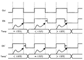
本発明の第1の実施形態では、被試験集積回路に内蔵される温度検出回路を用い、バーンイン試験条件を被試験集積回路間で精度良く揃え、初期不良品を効率よく選別できるバーンイン試験装置の構成および動作について説明する。
ここで、Taは恒温槽120により制御される雰囲気温度、Θjaは被試験集積回路1の熱抵抗値、Pは被試験集積回路1の消費電力である。従来手法では、接合温度Tjは直接測定されることは無く、演算式(1)により推定される。所望の接合温度Tjとするためには、既知である熱抵抗値Θjaを除いた、雰囲気温度Taと消費電力Pを所望の値に設定し、試験を行う。ここでは例えばΘja=50℃/W、Ta=125℃、P=1Wとすれば、Tj=175℃に設定される。
上記の式(2)では例えば、雰囲気温度TaのばらつきがΔTa=±5℃、熱抵抗値ΘjaのばらつきがΔΘja/Θja=±2%、消費電力PのばらつきがΔP/P=±2%であるとする。このとき接合温度Tjのばらつきの範囲はΔTj=±7℃となる。
本発明の第2の実施形態では、被試験集積回路に内蔵される温度検出回路を用い、バーンイン試験条件を被試験集積回路間で精度良く揃え、初期不良品を効率よく選別できるバーンイン試験装置において、バーンイン試験装置内の物理的配線量を削減できる構成および動作について説明する。
本発明の第3の実施形態では、被試験集積回路に内蔵される温度検出回路を用い、バーンイン試験条件を被試験集積回路間で精度良く揃え、初期不良品を効率よく選別できるバーンイン試験装置において、バーンイン試験装置内の物理的配線量を削減すると共に、被試験集積回路の内部における接合温度のばらつき影響を低減することで、均一な温度状態を実現できる構成および動作について説明する。
110…バーンインボード
120…恒温槽
1…被試験集積回路
2,2’…温度検出回路
3,3’…回路
4,5…制御回路
10…電源装置
20…試験制御装置
VDD…電源電圧
Temp,Temp’…温度情報信号
Ctrl…制御信号
EN、EN’…イネーブル信号
Claims (8)
- 恒温槽と、
前記恒温槽に配置され、複数の被試験集積回路を搭載するバーンインボードと、
複数の前記被試験集積回路に電源電圧を供給する電源装置と、
それぞれの前記被試験集積回路に内蔵され、それぞれの前記被試験集積回路の接合温度を測定する温度検出回路と、
複数の前記被試験集積回路の動作状態を制御するための第1の制御信号を複数の前記被試験集積回路に送信する試験制御装置と、
それぞれの前記被試験集積回路に内蔵され、それぞれの前記温度検出回路で測定される前記接合温度がバーンイン試験で設定された温度になるように前記第1の制御信号を補正し、補正された前記第1の制御信号を第2の制御信号として出力する制御回路と、
それぞれの前記被試験集積回路に内蔵され、前記第2の制御信号に応じて動作する回路と、
を備えることを特徴とするバーンイン試験装置。 - 請求項1に記載のバーンイン試験装置であって、
それぞれの前記制御回路は、
前記接合温度が前記バーンイン試験で設定された温度より高くなるにつれてそれぞれの前記被試験集積回路の消費電力を低くするように前記第1の制御信号を補正し、
前記接合温度が前記バーンイン試験で設定された温度より低くなるにつれてそれぞれの前記被試験集積回路の消費電力を高くするように前記第1の制御信号を補正する
ことを特徴とするバーンイン試験装置。 - 請求項1に記載のバーンイン試験装置であって、
前記第1の制御信号は、
パルス波形であり、
前記被試験集積回路は、
前記パルス波形に応じてON/OFFし、
それぞれの前記制御回路は、
前記接合温度が前記バーンイン試験で設定された温度より高くなるにつれてデューティ比を小さくするように前記第1の制御信号を補正し、
前記接合温度が前記バーンイン試験で設定された温度より低くなるにつれてデューティ比を大きくするように前記第1の制御信号を補正する
ことを特徴とするバーンイン試験装置。 - 請求項1に記載のバーンイン試験装置であって、
それぞれの前記温度検出回路は、
それぞれの前記回路の内部又はそれぞれの前記回路に隣接する位置に配置される
ことを特徴とするバーンイン試験装置。 - 請求項4に記載のバーンイン試験装置であって、
それぞれの前記制御回路は、
それぞれの前記温度検出回路によって測定される前記接合温度に応じた前記第2の制御信号を、それぞれの前記温度検出回路に対応するそれぞれの前記回路へ送信する
ことを特徴とするバーンイン試験装置。 - 請求項1に記載のバーンイン試験装置であって、
前記バーンインボードが複数搭載されている
ことを特徴とするバーンイン試験装置。 - 請求項1に記載のバーンイン試験装置に用いられるバーンイン試験方法であって、
それぞれの前記被試験集積回路に内蔵されるそれぞれの前記温度検出回路でそれぞれの前記被試験集積回路の接合温度を測定する温度検出工程と、
複数の前記被試験集積回路の動作状態を制御するための第1の制御信号を複数の前記被試験集積回路に送信する送信工程と、
それぞれの前記温度検出回路で測定される前記接合温度がバーンイン試験で設定された温度になるように前記第1の制御信号を補正する補正工程と、
を有することを特徴とするバーンイン試験方法。 - 請求項7に記載のバーンイン試験方法であって、
それぞれの前記温度検出回路によって測定される前記接合温度の精度を較正する工程をさらに有する
ことを特徴とするバーンイン試験方法。
Priority Applications (1)
| Application Number | Priority Date | Filing Date | Title |
|---|---|---|---|
| JP2015149667A JP6426552B2 (ja) | 2015-07-29 | 2015-07-29 | バーンイン試験装置及び方法 |
Applications Claiming Priority (1)
| Application Number | Priority Date | Filing Date | Title |
|---|---|---|---|
| JP2015149667A JP6426552B2 (ja) | 2015-07-29 | 2015-07-29 | バーンイン試験装置及び方法 |
Publications (2)
| Publication Number | Publication Date |
|---|---|
| JP2017032303A JP2017032303A (ja) | 2017-02-09 |
| JP6426552B2 true JP6426552B2 (ja) | 2018-11-21 |
Family
ID=57988522
Family Applications (1)
| Application Number | Title | Priority Date | Filing Date |
|---|---|---|---|
| JP2015149667A Active JP6426552B2 (ja) | 2015-07-29 | 2015-07-29 | バーンイン試験装置及び方法 |
Country Status (1)
| Country | Link |
|---|---|
| JP (1) | JP6426552B2 (ja) |
Families Citing this family (3)
| Publication number | Priority date | Publication date | Assignee | Title |
|---|---|---|---|---|
| KR20220114330A (ko) * | 2021-02-08 | 2022-08-17 | 한국전자기술연구원 | 동적열특성 평가를 이용한 정션 온도 세팅 반도체 소자의 신뢰성 시험 장치 및 방법 |
| CN116381283A (zh) * | 2022-07-20 | 2023-07-04 | 深圳市卓瑞源科技有限公司 | 充电模块老化的收纳组件及相应的老化装置 |
| CN116087748A (zh) * | 2022-12-31 | 2023-05-09 | 上海自动化仪表有限公司 | 电路板组装件自动热老化测试系统 |
Family Cites Families (7)
| Publication number | Priority date | Publication date | Assignee | Title |
|---|---|---|---|---|
| JPS6246274A (ja) * | 1985-08-23 | 1987-02-28 | Nec Corp | 高温バイアス試験装置 |
| JPH0536783A (ja) * | 1991-07-30 | 1993-02-12 | Sumitomo Electric Ind Ltd | バーンイン方法および装置 |
| US7103495B2 (en) * | 2004-09-17 | 2006-09-05 | Kabushiki Kaisha Toshiba | System and method for burn-in test control |
| JPWO2007023557A1 (ja) * | 2005-08-25 | 2009-02-26 | 株式会社アドバンテスト | 電子部品試験装置および電子部品試験装置における温度制御方法 |
| JP2007134442A (ja) * | 2005-11-09 | 2007-05-31 | Nec Electronics Corp | 半導体装置 |
| JP4315158B2 (ja) * | 2006-01-06 | 2009-08-19 | 住友電気工業株式会社 | デバイス評価装置およびデバイス評価方法 |
| US8384395B2 (en) * | 2010-05-06 | 2013-02-26 | Texas Instrument Incorporated | Circuit for controlling temperature and enabling testing of a semiconductor chip |
-
2015
- 2015-07-29 JP JP2015149667A patent/JP6426552B2/ja active Active
Also Published As
| Publication number | Publication date |
|---|---|
| JP2017032303A (ja) | 2017-02-09 |
Similar Documents
| Publication | Publication Date | Title |
|---|---|---|
| CN103207638B (zh) | 性能、热能及功率管理系统及其方法 | |
| CN101398692B (zh) | 电子系统 | |
| JP5405552B2 (ja) | 温度制御モジュール及びそれを含む温度制御装置 | |
| US20080186001A1 (en) | On-Chip Adaptive Voltage Compensation | |
| CN112345104B (zh) | 半导体器件、温度传感器和电源电压监测器 | |
| JP3783016B2 (ja) | 較正方法及びシステム | |
| US9608632B1 (en) | Resistance calibration method and related calibration system | |
| JP2016200570A (ja) | 半導体装置の電流検出方法および半導体装置 | |
| JP6426552B2 (ja) | バーンイン試験装置及び方法 | |
| JPWO2008020524A1 (ja) | 負荷変動補償回路、電子デバイス、試験装置、タイミング発生回路、及び負荷変動補償方法 | |
| TW201603479A (zh) | 具有校正功能之驅動裝置及其應用之無線充電驅動系統 | |
| JP2009210448A (ja) | 半導体装置 | |
| US20160054746A1 (en) | Voltage regulation system for integrated circuit | |
| US20190163221A1 (en) | Semiconductor device and current adjustment method in semiconductor device | |
| US8575994B2 (en) | Circuit and method for generating a clock signal | |
| EP4372342A1 (en) | Temperature sensor calibration for electronic devices | |
| TWI633286B (zh) | 溫度感測電路及其校正方法 | |
| US7714600B2 (en) | Load fluctuation correction circuit, electronic device, testing device, and timing generating circuit | |
| TWI824794B (zh) | 用於校正頻率飄移的校正裝置、方法與使用其的電子裝置 | |
| JP6942781B2 (ja) | 温度測定方法 | |
| JP4746489B2 (ja) | 半導体測定装置 | |
| CN114492286B (zh) | 控制芯片的方法及装置 | |
| TW201447312A (zh) | 晶片及具有該晶片的電路板 | |
| JP2007218812A (ja) | 電圧マージン試験方法 | |
| KR20120109190A (ko) | 온도 감지 회로 및 그 테스트 방법 |
Legal Events
| Date | Code | Title | Description |
|---|---|---|---|
| A621 | Written request for application examination |
Free format text: JAPANESE INTERMEDIATE CODE: A621 Effective date: 20170825 |
|
| A977 | Report on retrieval |
Free format text: JAPANESE INTERMEDIATE CODE: A971007 Effective date: 20180614 |
|
| A131 | Notification of reasons for refusal |
Free format text: JAPANESE INTERMEDIATE CODE: A131 Effective date: 20180619 |
|
| A521 | Request for written amendment filed |
Free format text: JAPANESE INTERMEDIATE CODE: A523 Effective date: 20180801 |
|
| TRDD | Decision of grant or rejection written | ||
| A01 | Written decision to grant a patent or to grant a registration (utility model) |
Free format text: JAPANESE INTERMEDIATE CODE: A01 Effective date: 20181009 |
|
| A61 | First payment of annual fees (during grant procedure) |
Free format text: JAPANESE INTERMEDIATE CODE: A61 Effective date: 20181025 |
|
| R150 | Certificate of patent or registration of utility model |
Ref document number: 6426552 Country of ref document: JP Free format text: JAPANESE INTERMEDIATE CODE: R150 |
|
| S533 | Written request for registration of change of name |
Free format text: JAPANESE INTERMEDIATE CODE: R313533 |
|
| R350 | Written notification of registration of transfer |
Free format text: JAPANESE INTERMEDIATE CODE: R350 |
|
| R250 | Receipt of annual fees |
Free format text: JAPANESE INTERMEDIATE CODE: R250 |
|
| R250 | Receipt of annual fees |
Free format text: JAPANESE INTERMEDIATE CODE: R250 |
|
| R250 | Receipt of annual fees |
Free format text: JAPANESE INTERMEDIATE CODE: R250 |