JP6426552B2 - Burn-in test apparatus and method - Google Patents
Burn-in test apparatus and method Download PDFInfo
- Publication number
- JP6426552B2 JP6426552B2 JP2015149667A JP2015149667A JP6426552B2 JP 6426552 B2 JP6426552 B2 JP 6426552B2 JP 2015149667 A JP2015149667 A JP 2015149667A JP 2015149667 A JP2015149667 A JP 2015149667A JP 6426552 B2 JP6426552 B2 JP 6426552B2
- Authority
- JP
- Japan
- Prior art keywords
- burn
- test
- under test
- temperature
- integrated circuit
- Prior art date
- Legal status (The legal status is an assumption and is not a legal conclusion. Google has not performed a legal analysis and makes no representation as to the accuracy of the status listed.)
- Active
Links
Images


Landscapes
- Tests Of Electronic Circuits (AREA)
- Testing Of Individual Semiconductor Devices (AREA)
Description
本発明は、集積回路装置のバーンイン試験装置及び方法に関する。 The present invention relates to an integrated circuit device burn-in test apparatus and method.
半導体集積回路におけるバーンイン試験は、主に被試験集積回路の初期不良を顕在化させ、これを選別可能とすることを目的とする。通常は、恒温槽内に複数の被試験集積回路を配置し、すべての被試験集積回路に対して等しいバーンイン条件を与えた上で、長期間に亘り試験を行う。 The burn-in test in a semiconductor integrated circuit is mainly intended to reveal an initial failure of the integrated circuit under test and make it possible to select it. Usually, a plurality of integrated circuits under test are placed in a constant temperature bath, and after giving equal burn-in conditions to all the integrated circuits under test, the test is performed for a long time.
近年、車載用途の半導体集積回路が多く利用されるようになってきたが、これらはその使用環境の過酷さから、求められる信頼度は日を追うごとに高くなっている。ある場合においては、バーンイン試験中における被試験集積回路の接合温度条件は150℃以上が設定される。 In recent years, semiconductor integrated circuits for in-vehicle use have come to be widely used, but due to the severeness of their use environment, the required reliability increases with the passing of days. In some cases, the junction temperature condition of the integrated circuit under test during the burn-in test is set to 150 ° C. or higher.
また一般に、バーンイン試験中は被試験集積回路の温度は一定であることが求められる。 Generally, the temperature of the integrated circuit under test is required to be constant during the burn-in test.
条件がばらついた状態で試験を実施すれば、過剰に試験状態に晒された集積回路は経年劣化により不良に至る恐れがあり、逆に、十分に試験されない状態で出荷されれば、出荷後に初期不良が顕在化する恐れもある。 If the test is conducted under different conditions, integrated circuits exposed to excessive test conditions may lead to failure due to aging, and conversely, if they are shipped without being sufficiently tested, the initial stage after shipment There is also a possibility that defects will be apparent.
このような問題を解決するために、試験対象である複数の半導体装置のジャンクション温度(接合温度)を精度良く制御することができる半導体装置の試験装置が知られている(例えば、特許文献1参照)。 In order to solve such a problem, there is known a test apparatus for a semiconductor device capable of accurately controlling junction temperatures (junction temperatures) of a plurality of semiconductor devices to be tested (see, for example, Patent Document 1) ).
特許文献1に開示されるような技術では、試験対象となる半導体装置毎に、個別に温度センサと送風ファンとを配置する必要があるため、バーンイン試験装置内の配線が複雑化すると共に装置コスト増加を招いてしまう。また、接合温度を測定するための温度センサはヒートシンクの内部に配置されており、その測定精度については疑問が残る。
In the technology disclosed in
本発明の目的は、配線量を削減しつつ、高精度で接合温度のばらつきを低減することができるバーンイン試験装置及び方法を提供することにある。 An object of the present invention is to provide a burn-in test apparatus and method that can reduce variations in junction temperature with high accuracy while reducing the amount of wiring.
上記目的を達成するために、本発明は、恒温槽と、前記恒温槽に配置され、複数の被試験集積回路を搭載するバーンインボードと、複数の前記被試験集積回路に電源電圧を供給する電源装置と、それぞれの前記被試験集積回路に内蔵され、それぞれの前記被試験集積回路の接合温度を測定する温度検出回路と、複数の前記被試験集積回路の動作状態を制御するための第1の制御信号を複数の前記被試験集積回路に送信する試験制御装置と、それぞれの前記被試験集積回路に内蔵され、それぞれの前記温度検出回路で測定される前記接合温度がバーンイン試験で設定された温度になるように前記第1の制御信号を補正し、補正された前記第1の制御信号を第2の制御信号として出力する制御回路と、それぞれの前記被試験集積回路に内蔵され、前記第2の制御信号に応じて動作する回路と、を備える。
To achieve the above object, the present invention comprises a constant temperature bath, the disposed in a constant temperature bath, the power supply and the burn-in board for mounting a plurality of integrated circuit under test, the power supply voltage to a plurality of said integrated circuit under test a device, incorporated in each of the integrated circuit under test, a temperature detection circuit for measuring the junction temperature of each of the integrated circuit under test, for controlling the operating state of the plurality of the integrated circuit under test first A test control device for transmitting control signals to a plurality of the integrated circuits under test, and a temperature set in a burn-in test, wherein the junction temperature measured in each of the temperature detection circuits is incorporated in each integrated circuit under test the first corrected control signal, and a control circuit for outputting a corrected first control signal as a second control signal, is incorporated in each of the integrated circuit under test so that, And a circuit which operates in response to serial second control signal.
本発明によれば、配線量を削減しつつ、高精度で接合温度のばらつきを低減することができるバーンイン試験装置及び方法を提供することにある。上記した以外の課題、構成及び効果は、以下の実施形態の説明により明らかにされる。 According to the present invention, it is an object of the present invention to provide a burn-in test apparatus and method capable of reducing variation in junction temperature with high accuracy while reducing the amount of wiring. Problems, configurations, and effects other than those described above will be apparent from the description of the embodiments below.
以下、図面を参照しつつ、本発明の実施の形態について説明する。なお、図面は簡略的なものであるから、この図面の記載を根拠として本発明の技術的範囲を狭く解釈してはならない。また、同一の要素には、同一の符号を付し、重複する説明は省略する。 Hereinafter, embodiments of the present invention will be described with reference to the drawings. Note that the drawings are simplified, and therefore the technical scope of the present invention should not be narrowly interpreted based on the description of the drawings. In addition, the same reference numerals are given to the same elements, and duplicate explanations are omitted.
(第1の実施形態)
本発明の第1の実施形態では、被試験集積回路に内蔵される温度検出回路を用い、バーンイン試験条件を被試験集積回路間で精度良く揃え、初期不良品を効率よく選別できるバーンイン試験装置の構成および動作について説明する。
First Embodiment
In a first embodiment of the present invention, a burn-in test apparatus is provided which can accurately align burn-in test conditions among integrated circuits under test using a temperature detection circuit incorporated in the integrated circuit under test and efficiently sort out initial failure products. The configuration and operation will be described.
図1は本発明の第1の実施形態であるバーンイン試験装置100の構成を示すブロック図である。
FIG. 1 is a block diagram showing the configuration of a burn-in
図1に示すバーンイン試験装置100は、被試験集積回路1と、被試験集積回路1の動作を制御するための試験制御装置20と、被試験集積回路1に内蔵される温度検出回路2と、複数の被試験集積回路1を搭載したバーンインボード110と、被試験集積回路1に電源電圧VDDを供給するための電源装置10と、から構成される。
The burn-in
図1による構成では、単体のバーンインボード110がバーンイン試験装置100に搭載されている例が示されているが、バーンインボード110はバーンイン試験装置100に複数個搭載されていても良い。
In the configuration according to FIG. 1, an example is shown in which a single burn-in
バーンインボード110は例えば、設定温度の調整が可能な、恒温槽120の内部に配置される。被試験集積回路1は一般に樹脂材あるいは無機焼結材を用いた封止材により封止され、図示しないソケットを介してバーンインボード110に搭載される。
The burn-in
すなわち、バーンイン試験装置100は、恒温槽120を備える。バーンインボード110は、恒温槽120に配置され、被試験集積回路1を搭載する。バーンインボード110には、複数の被試験集積回路1が搭載されている。
That is, burn-in
本実施形態において温度検出回路2は、被試験集積回路1に内蔵されていることを特徴とし、被試験集積回路1の接合温度Tjに比例した値を検出し、温度情報信号Tempに変換して出力する機能を有する。すなわち、温度検出回路2は、被試験集積回路1に内蔵され、被試験集積回路1の接合温度を測定する。
In the present embodiment, the
温度情報信号Tempは、シングルビットのシリアルデータあるいは多ビットのデジタルデータのいずれの出力形式を採っても良い。温度情報信号Tempは、任意の通信手段によって試験制御装置20へ送信される。
The temperature information signal Temp may take the form of either single-bit serial data or multi-bit digital data. The temperature information signal Temp is transmitted to the
また温度検出回路2は、被試験集積回路1の製造工程において温度検出精度の較正が実施されていることを特徴とする。図2は、本発明の第1の実施形態に係る、被試験集積回路1の製造工程の一例を示すフローチャートである。
The
図2のフローチャートに示すウェハ製造工程(S10)においては、ウェハ上の複数の領域に前記被試験集積回路1をそれぞれ形成する。ウェハ上に形成された複数の被試験集積回路1に対しては、ウェハ状態においてそれぞれ試験を実施する(S15)。ウェハ試験における、被試験集積回路1に対する試験項目には種々のものが考えられ得る一方で、内蔵する温度検出回路2の較正を行うこともできる(S15)。すなわちこの工程において、温度検出回路2の温度検出精度は所望の値に調整できる。
In the wafer manufacturing process (S10) shown in the flowchart of FIG. 2, the integrated circuit under
続いて、被試験集積回路1のパッケージの組み立て、封止が行われ(S20)、組み立てられた被試験集積回路1を用いてバーンイン試験が行われる(S25)。そして、所定の最終出荷試験が行われる(S30)。なお、バーンイン試験(S25)の詳細は、図3を用いて後述する。
Subsequently, the package of the integrated circuit under
温度検出回路2が動作する状況は、バーンイン試験中(S25)に限られるものではない。温度検出回路2の出力である温度情報信号Tempは、被試験集積回路1の内部回路の制御に使用することも可能である。従って、温度検出回路2はバーンイン試験以外の場合において動作していても差し支えない。
The situation in which the
図1に戻り、試験制御装置20は、被試験集積回路1の動作制御を行う。試験制御装置20は、電源装置10を制御して複数の被試験集積回路1に対する電源供給(電源電圧VDD)を実施する他、被試験集積回路1を所望の動作状態へ遷移させるために、被試験集積回路1に対して制御信号Ctrlを送信することにより制御する機能を有する。試験制御装置20はまた、温度検出回路2より温度情報Temp(温度情報信号)を受信し、被試験集積回路1の動作状態を修正するために制御信号Ctrlを送信する機能も有する。
Returning to FIG. 1, the
換言すれば、試験制御装置20は、被試験集積回路1の動作状態を制御するための制御信号Ctrl(第1の制御信号)を被試験集積回路1に送信する送信部と、温度検出回路2で測定される接合温度Tjがバーンイン試験で設定された温度になるように制御信号Ctrlを補正する補正部として機能する。
In other words, the
電源装置10は、複数の被試験集積回路1に電源電圧VDDを供給する機能を有する。電源装置10のオン・オフおよび電源電圧VDDの電圧値は、試験制御装置20から制御される。
The
まず、従来方法としての、バーンイン試験中における接合温度Tjの調整手段と、その手段を用いた場合の接合温度Tjの誤差について説明する。一般に、被試験集積回路1の接合温度Tjは下記の演算式(1)により求められる。
First, as a conventional method, means for adjusting the junction temperature Tj during burn-in test and errors in the junction temperature Tj when the means are used will be described. Generally, the junction temperature Tj of the integrated circuit under
Tj=Ta+Θja×P …(1)
ここで、Taは恒温槽120により制御される雰囲気温度、Θjaは被試験集積回路1の熱抵抗値、Pは被試験集積回路1の消費電力である。従来手法では、接合温度Tjは直接測定されることは無く、演算式(1)により推定される。所望の接合温度Tjとするためには、既知である熱抵抗値Θjaを除いた、雰囲気温度Taと消費電力Pを所望の値に設定し、試験を行う。ここでは例えばΘja=50℃/W、Ta=125℃、P=1Wとすれば、Tj=175℃に設定される。
Tj = Ta + Θja × P (1)
Here, Ta is the ambient temperature controlled by the
しかしながら、雰囲気温度Ta、熱抵抗値Θja、消費電力Pはそれぞれ以下に例として挙げる要因に起因して誤差を持ち得る。これらの要因は、雰囲気温度Taに関しては例えば恒温槽120内における温度不均一性であり、熱抵抗値Θjaに関しては例えば被試験集積回路1の封止材の寸法ばらつきであり、消費電力Pに関しては例えば被試験集積回路1の製造ばらつき、などである。従って、演算式(1)により求められる接合温度Tjにも誤差が内包されることは容易に想像できる。
However, the ambient temperature Ta, the thermal resistance value Θja, and the power consumption P may have errors due to factors listed below as examples. These factors are, for example, the temperature non-uniformity in the
接合温度Tjの誤差ΔTjを式(1)より求めると、下記の式(2)で表される。ただし、2次の項については無視する。 The error ΔTj of the junction temperature Tj is calculated by the equation (1), and is represented by the following equation (2). However, the second term is ignored.
ΔTj=ΔTa+ΔΘja×P+Θja×ΔP …(2)
上記の式(2)では例えば、雰囲気温度TaのばらつきがΔTa=±5℃、熱抵抗値ΘjaのばらつきがΔΘja/Θja=±2%、消費電力PのばらつきがΔP/P=±2%であるとする。このとき接合温度Tjのばらつきの範囲はΔTj=±7℃となる。
ΔTj = ΔTa + ΔΘja × P + Θja × ΔP (2)
In the above equation (2), for example, the variation of the ambient temperature Ta is ΔTa = ± 5 ° C., the variation of the thermal resistance value Θja is ΔΘja / Θja = ± 2%, and the variation of the power consumption P is ΔP / P = ± 2% Suppose that there is. At this time, the range of variation of the junction temperature Tj is ΔTj = ± 7 ° C.
次に、本発明の第1の実施形態のバーンイン試験装置100における接合温度Tj調整手段について、試験制御装置20の制御フローを交えて説明する。図3は、バーンイン試験における試験制御装置20の制御フローの一例を示したものである。
Next, the junction temperature Tj adjusting means in the burn-in
バーンイン試験を開始すると、試験制御装置20は被試験集積回路1の動作を開始させる(S100)。被試験集積回路1に内蔵される温度検出回路2は、被試験集積回路1の接合温度Tjを検出し、温度情報Tempに変換した上で送信し、試験制御装置20が受信する(S105)。
When the burn-in test is started, the
温度情報Tempを受信した試験制御装置20は、Tempに対応する接合温度Tjと、バーンイン条件の設定値とに関して大小比較を実施する(S110)。接合温度Tjがバーンイン条件の設定値よりも大きい場合(S110:YES)は、被試験集積回路1の消費電力Pを低減するように動作状態を制御する(S115)。逆に接合温度Tjがバーンイン条件の設定値よりも小さい場合(S110:NO)には、被試験集積回路1の消費電力Pを上げるように動作状態を制御する(S120)。バーンイン試験が継続される場合(S125:NO)は、試験制御装置20が温度情報Tempを受信するフローへと戻り、そうでない場合(S125:YES)は終了する。
The
換言すれば、試験制御装置20は、接合温度Tjがバーンイン試験で設定された温度より高くなるにつれて被試験集積回路1の消費電力を低くするように制御信号Ctrl(第1の制御信号)を補正し、接合温度Tjがバーンイン試験で設定された温度より低くなるにつれて被試験集積回路1の消費電力を高くするように制御信号Ctrlを補正する補正部として機能する。
In other words, the
例えば、制御信号Ctrl(第1の制御信号)は、パルス波形であり、被試験集積回路1は、パルス波形に応じてON/OFFする。ここで、試験制御装置20(補正部)は、接合温度Tjがバーンイン試験で設定された温度より高くなるにつれてデューティ比を小さくするように制御信号Ctrlを補正し、接合温度Tjがバーンイン試験で設定された温度より低くなるにつれてデューティ比を大きくするように制御信号Ctrlを補正するようにしてもよい。
For example, the control signal Ctrl (first control signal) is a pulse waveform, and the integrated circuit under
本発明の第1の実施形態におけるバーンイン条件は、例えば前述の従来手法の場合と同様に熱抵抗値Θja=50℃/W、雰囲気温度Ta=125℃、消費電力P=1Wとし、接合温度Tj=175℃に設定されるものとする。このときも従来手法の場合と同様に雰囲気温度Taと熱抵抗値Θja、および消費電力Pにはばらつき要因が内在する。しかし、本実施形態においては被試験集積回路1の接合温度Tjを、温度検出回路2が直接検出するため、温度検出回路2の検出精度のみが接合温度TjのばらつきΔTjに影響する。すなわち、雰囲気温度Taや熱抵抗値Θja、および消費電力Pによるばらつき要因を排除できる。
The burn-in conditions in the first embodiment of the present invention are, for example, the thermal resistance value Θja = 50 ° C./W, the ambient temperature Ta = 125 ° C., and the power consumption P = 1 W as in the conventional method described above. It shall be set to = 175 ° C. Also in this case, as in the case of the conventional method, variation factors are inherent in the ambient temperature Ta, the thermal resistance value Θja, and the power consumption P. However, in the present embodiment, since the
本発明の第1の実施形態において、温度検出回路2の検出精度が、例えば±2℃以内に較正されているとすると、接合温度Tjも同様に±2℃以内に制御できる。これは従来の接合温度Tj調整方法における誤差ΔTj=±7℃よりも良い精度である。また、被試験集積回路1の消費電力Pを個別に調整することで、複数の被試験集積回路間における接合温度Tjばらつきを抑えることも容易となる。
In the first embodiment of the present invention, assuming that the detection accuracy of the
以上説明したように、本実施形態によれば、配線量を削減しつつ、高精度で接合温度のばらつきを低減することができる。 As described above, according to the present embodiment, it is possible to reduce variation in junction temperature with high accuracy while reducing the amount of wiring.
すなわち、被試験集積回路に内蔵される温度検出回路を用い、バーンイン試験条件を被試験集積回路間で精度良く揃え、初期不良品を効率よく選別できるバーンイン試験装置が提供できる。 That is, it is possible to provide a burn-in test apparatus capable of efficiently sorting out initial defective products by accurately aligning burn-in test conditions among integrated circuits under test using a temperature detection circuit incorporated in the integrated circuit under test.
(第2の実施形態)
本発明の第2の実施形態では、被試験集積回路に内蔵される温度検出回路を用い、バーンイン試験条件を被試験集積回路間で精度良く揃え、初期不良品を効率よく選別できるバーンイン試験装置において、バーンイン試験装置内の物理的配線量を削減できる構成および動作について説明する。
Second Embodiment
In a second embodiment of the present invention, a burn-in test apparatus capable of efficiently aligning burn-in test conditions among integrated circuits under test using a temperature detection circuit incorporated in the integrated circuit under test and efficiently sorting out initial failure products. The configuration and operation that can reduce the amount of physical wiring in the burn-in test apparatus will be described.
図4は本発明の第2の実施形態であるバーンイン試験装置100の構成を示すブロック図である。
FIG. 4 is a block diagram showing the configuration of a burn-in
図4に示すバーンイン試験装置100は、被試験集積回路1と、被試験集積回路1の動作を制御するための試験制御装置20と、被試験集積回路1に内蔵される回路3と、被試験集積回路1に内蔵され、回路3に近接して配置されていることを特徴とする温度検出回路2と、被試験集積回路1に内蔵され、回路3の動作を制御することを特徴とする制御回路4と、複数の被試験集積回路1を搭載したバーンインボード110と、被試験集積回路1に電源電圧VDDを供給するための電源装置10と、から構成される。
The burn-in
図4による構成では、単体のバーンインボード110がバーンイン試験装置100に搭載されている例が示されているが、バーンインボード110はバーンイン試験装置100に複数個搭載されていても良い。
In the configuration according to FIG. 4, an example is shown in which a single burn-in
本実施形態において温度検出回路2は、被試験集積回路1に内蔵されており、回路3に近接して配置されていることを特徴とし、回路3の近傍における、被試験集積回路1の接合温度Tjに比例した値を検出し、温度情報信号Tempに変換して出力する機能を有する。温度情報信号Tempは、シングルビットのシリアルデータあるいは多ビットのデジタルデータのいずれの出力形式を採っても良い。温度情報信号Tempは、被試験集積回路1の内部の配線を通して制御回路4へ送信される。
In the present embodiment, the
試験制御装置20は、電源装置10を制御して複数の被試験集積回路1に対する電源供給を実施する他、制御回路4に対して制御信号Ctrlを送信する機能を有する。
The
制御回路4は、被試験集積回路1に内蔵されていることを特徴としており、温度検出回路2から温度情報Tempを受信し、Tempに対応する接合温度Tjと、バーンイン条件として予め設定されている温度とを比較する。その比較結果によって、試験制御装置20から受信した制御信号Ctrlに変調を加え、回路3の動作状態を制御するイネーブル信号ENとして出力する機能を有する。
The
換言すれば、制御回路4は、温度検出回路2で測定される接合温度Tjがバーンイン試験で設定された温度になるように制御信号Ctrl(第1の制御信号)を補正し、補正された制御信号Ctrlをイネーブル信号EN(第2の制御信号)して出力する補正部として機能する。
In other words, the
回路3は、被試験集積回路1に内蔵されていることを特徴としており、その動作状態はイネーブル信号ENによって制御されることを特徴とする。すなわち、被試験集積回路1は、イネーブル信号EN(第2の制御信号)に応じて動作する回路3を内蔵する。温度検出回路2は、回路3の内部又は回路3に隣接する位置に配置される。
The
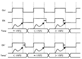
ここで、本発明の第2の実施形態において被試験集積回路1の接合温度Tjを精度良く調整する方法について、例を挙げつつ説明する。バーンイン条件は例えば、第1の実施形態における条件と同様に雰囲気温度Ta=125℃、熱抵抗値Θja=50℃/W、消費電力P=1Wとし、接合温度Tj=175℃に設定されているものとする。図5には、本発明の第2に実施形態における、被試験集積回路1の内部信号のタイムチャートを示す。図5における信号名は、それぞれ図4に記載されているものに対応する。
Here, a method of accurately adjusting the junction temperature Tj of the integrated circuit under
制御信号Ctrlは例えば、図5に示すように周期的に、論理レベルがハイおよびローとなる期間を交互に繰り返すものとする。制御信号Ctrlにおけるディーティ比は、例えば50%であるとする。温度情報Tempは、制御信号Ctrlに対して独立に、ある周期で出力値が更新されるものとする。 For example, as shown in FIG. 5, the control signal Ctrl alternately repeats periods in which the logic level is high and low. The duty ratio in the control signal Ctrl is, for example, 50%. It is assumed that the output value of temperature information Temp is updated at a certain cycle independently of control signal Ctrl.
回路3は、入力されるイネーブル信号ENの論理レベルがハイである期間は動作し、消費電力が発生する。イネーブル信号ENの論理レベルがローである期間において回路3は動作せず、消費電力はほぼ0となる。
The
制御回路4は、制御信号Ctrlと温度情報信号Tempをそれぞれ受信し、回路3に対してイネーブル信号ENを出力する。その際、温度情報信号Tempとバーンイン条件、すなわち接合温度Tj=175℃との比較を行う。その比較結果に従い、制御信号Ctrlのデューティ比を基準として変更を加え、イネーブル信号ENとして出力する。
The
例を図5に示すが、Tempの示す値が175℃に等しい場合は、制御回路4はデューティ比を変更せずにイネーブル信号ENを出力する。Tempの示す値が175℃を下回る場合はデューティ比を上昇させ、175℃を上回る場合にはデューディ比を低下させる。
An example is shown in FIG. 5, but when the value indicated by Temp is equal to 175 ° C., the
前記制御回路4によってイネーブル信号ENのデューティ比が変更されると、一周期中における消費電力も変動する。具体的には、ディーティ比が上昇すれば回路3が動作する期間が延びることから一周期における消費電力も増加し、ディーティ比が低下すればその逆であり消費電力は減少する。故に、これは演算式(1)における消費電力Pを調整できることに他ならない。
When the duty ratio of the enable signal EN is changed by the
また、本実施形態において示した接合温度Tjの調整手法では、温度情報信号Tempは被試験集積回路1の内部において送受信されるのみである。従って、被試験集積回路1の外部に出力するための端子や、バーンイン試験装置100の内部配線数を削減することができる。
Further, in the method of adjusting the junction temperature Tj shown in the present embodiment, the temperature information signal Temp is only transmitted and received inside the integrated circuit under
以上説明したように、本実施形態によれば、配線量を削減しつつ、高精度で接合温度のばらつきを低減することができる。 As described above, according to the present embodiment, it is possible to reduce variation in junction temperature with high accuracy while reducing the amount of wiring.
すなわち、被試験集積回路1に内蔵される温度検出回路2を用い、バーンイン試験条件を被試験集積回路間で精度良く揃え、初期不良品を効率よく選別できるバーンイン試験装置100において、バーンイン試験装置内の物理的配線量を削減できる。
That is, in the burn-in
(第3の実施形態)
本発明の第3の実施形態では、被試験集積回路に内蔵される温度検出回路を用い、バーンイン試験条件を被試験集積回路間で精度良く揃え、初期不良品を効率よく選別できるバーンイン試験装置において、バーンイン試験装置内の物理的配線量を削減すると共に、被試験集積回路の内部における接合温度のばらつき影響を低減することで、均一な温度状態を実現できる構成および動作について説明する。
Third Embodiment
In a third embodiment of the present invention, a burn-in test apparatus capable of efficiently aligning burn-in test conditions among integrated circuits under test using a temperature detection circuit incorporated in the integrated circuit under test and efficiently sorting out initial failure products. An arrangement and operation capable of realizing a uniform temperature state by reducing the amount of physical wiring in the burn-in test apparatus and reducing the influence of variations in junction temperature inside the integrated circuit under test will be described.
図6は本発明の第3の実施形態であるバーンイン試験装置100の構成を示すブロック図である。
FIG. 6 is a block diagram showing the configuration of a burn-in
図6に示すバーンイン試験装置100は、被試験集積回路1と、被試験集積回路1の動作を制御するための試験制御装置20と、被試験集積回路1に内蔵される回路3と、被試験集積回路1に内蔵され、回路3に近接して配置されていることを特徴とする温度検出回路2と、被試験集積回路1に内蔵され、回路3とは離れた場所に配置されていることを特徴とする回路3’と、被試験集積回路1に内蔵され、回路3’に近接して配置されていることを特徴とする温度検出回路2’と、被試験集積回路1に内蔵され、回路3と回路3’の動作を独立に制御することを特徴とする制御回路5と、複数の被試験集積回路1を搭載したバーンインボード110と、被試験集積回路1に電源電圧VDDを供給するための電源装置10と、から構成される。
The burn-in
図6による構成では、単体のバーンインボード110がバーンイン試験装置100に搭載されている例が示されているが、バーンインボード110はバーンイン試験装置100に複数個搭載されていても良い。
In the configuration according to FIG. 6, an example is shown in which a single burn-in
なお、例えば温度検出回路2と2’、回路3と3’、温度情報信号TempとTemp’のように記号(’)を付した要素とそうでない要素は、互いに同一の特徴を有しており、電気的接続関係などは記号の有無による違いのみであることを理解されたい。
For example, elements with symbols (') such as
本実施形態において温度検出回路2’は、被試験集積回路1に内蔵されており、回路3’に近接して配置されていることを特徴とし、回路3’の付近における、被試験集積回路1の接合温度Tj’に比例した値を検出し、温度情報信号Temp’に変換して出力する機能を有する。温度情報信号Temp’は、被試験集積回路1の内部の配線を通して制御回路5へ送信される。
In the present embodiment, the temperature detection circuit 2 'is incorporated in the integrated circuit under
換言すれば、回路3及び温度検出回路2は、それぞれ複数ある。制御回路5は、それぞれの温度検出回路2、2’によって測定される接合温度Tj、Tj’に応じたイネーブル信号EN(第2の制御信号)を、温度検出回路2、2’に対応する回路3、3’へ送信する。
In other words, there are a plurality of
本実施形態において試験制御装置20は、電源装置10を制御して複数の被試験集積回路1に対する電源供給を実施する他、制御回路5に対して制御信号Ctrlを送信する機能を有する。
In the present embodiment, the
制御回路5は、被試験集積回路1に内蔵されていることを特徴としており、温度検出回路2および2’から温度情報TempおよびTemp’を受信し、それぞれに対応する接合温度TjおよびTj’と、バーンイン条件として予め設定されている温度とを、それぞれ比較する。その比較結果によって、試験制御装置20から受信した制御信号Ctrlに変調を加え、回路3の動作状態を制御するイネーブル信号ENと、回路3’の動作状態を制御するイネーブル信号EN’として独立に出力する機能を有する。
ここで、本発明の第3の実施形態において被試験集積回路1の接合温度Tjを精度良く調整する方法について、例を挙げつつ説明する。同一記号の要素やバーンイン条件は、本発明の第2の実施形態と同様の状態をとるものとして、以降では説明を省略する。図7には、本発明の第3に実施形態における、被試験集積回路1の内部信号のタイムチャートを示す。図7における信号名は、それぞれ図6に記載されているものに対応する。
Here, a method of precisely adjusting the junction temperature Tj of the integrated circuit under
制御回路5は、制御信号Ctrlと温度情報信号TempおよびTemp’をそれぞれ受信し、回路3に対してイネーブル信号ENを、回路3’に対してイネーブル信号EN’を出力する。その際、温度情報信号TempおよびTemp’とバーンイン条件、すなわち接合温度Tj=175℃との比較を行う。その比較結果に従い、制御信号Ctrlのデューティ比を基準として変更を加え、イネーブル信号ENおよびEN’として独立に出力する。
The
例を図7に示すが、Tempの示す値が175℃に等しい場合は、制御回路5はデューティ比を変更せずにイネーブル信号ENを出力する。Tempの示す値が175℃を下回る場合はデューティ比を上昇させ、175℃を上回る場合にはデューディ比を低下させる。制御回路5はまた、Temp’の値を基準として同様の制御を行い、イネーブル信号EN’を出力する。
An example is shown in FIG. 7, but when the value indicated by Temp is equal to 175 ° C., the
ところで、接合温度TjとTj’は被試験集積回路1においてそれぞれ異なる箇所で接合温度を検出したものであるが、これらの値に相違があれば被試験集積回路内で接合温度のばらつきや勾配が存在することになる。このとき、制御回路5によりENとEN’を独立に制御することで、接合温度TjとTj’をそれぞれ個別に175℃に近づける制御することができるようになり、被試験集積回路1の内部における接合温度を均一にすることが可能である。
By the way, although the junction temperatures Tj and Tj 'are obtained by detecting the junction temperatures at different points in the integrated circuit under
以上説明したように、本実施形態によれば、配線量を削減しつつ、高精度で接合温度のばらつきを低減することができる。 As described above, according to the present embodiment, it is possible to reduce variation in junction temperature with high accuracy while reducing the amount of wiring.
すなわち、被試験集積回路1に内蔵される温度検出回路2を用い、バーンイン試験条件を被試験集積回路間で精度良く揃え、初期不良品を効率よく選別できるバーンイン試験装置100において、バーンイン試験装置内の物理的配線量を削減すると共に、被試験集積回路1の内部における接合温度のばらつき影響を低減することで、均一な温度状態を実現できる。
That is, in the burn-in
なお、本発明は上記の実施形態に限定されるものではなく、様々な変形例が含まれる。例えば、上記した実施形態は本発明を分かりやすく説明するために詳細に説明したものであり、必ずしも説明した全ての構成を備えるものに限定されるものではない。また、ある実施形態の構成の一部を他の実施形態の構成に置き換える事が可能であり、また、ある実施形態の構成に他の実施形態の構成を加えることも可能である。また、各実施形態の構成の一部について他の構成の追加・削除・置換をする事が可能である。 The present invention is not limited to the above embodiment, but includes various modifications. For example, the above-described embodiment is described in detail to explain the present invention in an easy-to-understand manner, and is not necessarily limited to one having all the described configurations. In addition, part of the configuration of one embodiment can be replaced with the configuration of another embodiment, and the configuration of another embodiment can be added to the configuration of one embodiment. In addition, it is possible to add, delete, and replace another configuration for part of the configuration of each embodiment.
また、制御線や信号線は説明上必要と考えられるものを示しており、製品上必ずしも全ての制御線や信号線を示しているとは限らない。 Further, the control lines and the signal lines indicate what is considered to be necessary for the description, and not all the control lines and the signal lines in the product are necessarily shown.
100…バーンイン試験装置
110…バーンインボード
120…恒温槽
1…被試験集積回路
2,2’…温度検出回路
3,3’…回路
4,5…制御回路
10…電源装置
20…試験制御装置
VDD…電源電圧
Temp,Temp’…温度情報信号
Ctrl…制御信号
EN、EN’…イネーブル信号
100 burn-in
Claims (8)
前記恒温槽に配置され、複数の被試験集積回路を搭載するバーンインボードと、
複数の前記被試験集積回路に電源電圧を供給する電源装置と、
それぞれの前記被試験集積回路に内蔵され、それぞれの前記被試験集積回路の接合温度を測定する温度検出回路と、
複数の前記被試験集積回路の動作状態を制御するための第1の制御信号を複数の前記被試験集積回路に送信する試験制御装置と、
それぞれの前記被試験集積回路に内蔵され、それぞれの前記温度検出回路で測定される前記接合温度がバーンイン試験で設定された温度になるように前記第1の制御信号を補正し、補正された前記第1の制御信号を第2の制御信号として出力する制御回路と、
それぞれの前記被試験集積回路に内蔵され、前記第2の制御信号に応じて動作する回路と、
を備えることを特徴とするバーンイン試験装置。 Constant temperature bath,
A burn-in board disposed in the constant temperature bath and carrying a plurality of integrated circuits under test;
A power supply device for supplying a power supply voltage to a plurality of the integrated circuits under test;
Built in each of the integrated circuit under test, a temperature detection circuit for measuring the junction temperature of each of the integrated circuit under test,
A test controller for transmitting a first control signal for controlling the operation states of the plurality of the integrated circuit under test to a plurality of said integrated circuit under test,
Built in each of the integrated circuit under test, the said bonding temperature measured at each of said temperature detection circuit corrects the first control signal so that the temperature set by the burn-in test, the corrected A control circuit that outputs a first control signal as a second control signal ;
A circuit incorporated in each of the integrated circuits under test and operating according to the second control signal;
A burn-in test apparatus comprising:
それぞれの前記制御回路は、
前記接合温度が前記バーンイン試験で設定された温度より高くなるにつれてそれぞれの前記被試験集積回路の消費電力を低くするように前記第1の制御信号を補正し、
前記接合温度が前記バーンイン試験で設定された温度より低くなるにつれてそれぞれの前記被試験集積回路の消費電力を高くするように前記第1の制御信号を補正する
ことを特徴とするバーンイン試験装置。 The burn-in test apparatus according to claim 1, wherein
Each said control circuit is
Correcting the first control signal to lower the power consumption of each of the integrated circuits under test as the junction temperature becomes higher than the temperature set in the burn-in test;
A burn-in test apparatus, comprising: correcting the first control signal so as to increase power consumption of each of the integrated circuits under test as the junction temperature becomes lower than a temperature set in the burn-in test.
前記第1の制御信号は、
パルス波形であり、
前記被試験集積回路は、
前記パルス波形に応じてON/OFFし、
それぞれの前記制御回路は、
前記接合温度が前記バーンイン試験で設定された温度より高くなるにつれてデューティ比を小さくするように前記第1の制御信号を補正し、
前記接合温度が前記バーンイン試験で設定された温度より低くなるにつれてデューティ比を大きくするように前記第1の制御信号を補正する
ことを特徴とするバーンイン試験装置。 The burn-in test apparatus according to claim 1, wherein
The first control signal is
It is a pulse waveform,
The integrated circuit under test is
ON / OFF according to the pulse waveform,
Each said control circuit is
Correcting the first control signal to reduce the duty ratio as the junction temperature becomes higher than the temperature set in the burn-in test;
A burn-in test apparatus, comprising: correcting the first control signal to increase a duty ratio as the junction temperature becomes lower than a temperature set in the burn-in test.
それぞれの前記温度検出回路は、
それぞれの前記回路の内部又はそれぞれの前記回路に隣接する位置に配置される
ことを特徴とするバーンイン試験装置。 The burn-in test apparatus according to claim 1 , wherein
Each of the temperature detection circuits
The burn-in test apparatus is disposed at a position inside or adjacent to each of the circuits.
それぞれの前記制御回路は、
それぞれの前記温度検出回路によって測定される前記接合温度に応じた前記第2の制御信号を、それぞれの前記温度検出回路に対応するそれぞれの前記回路へ送信する
ことを特徴とするバーンイン試験装置。 The burn-in test apparatus according to claim 4 , wherein
Each said control circuit is
A burn-in test apparatus comprising: transmitting the second control signal according to the junction temperature measured by each of the temperature detection circuits to each of the circuits corresponding to each of the temperature detection circuits.
前記バーンインボードが複数搭載されている
ことを特徴とするバーンイン試験装置。 The burn-in test apparatus according to claim 1, wherein
A plurality of burn-in boards are mounted. A burn-in test apparatus.
それぞれの前記被試験集積回路に内蔵されるそれぞれの前記温度検出回路でそれぞれの前記被試験集積回路の接合温度を測定する温度検出工程と、
複数の前記被試験集積回路の動作状態を制御するための第1の制御信号を複数の前記被試験集積回路に送信する送信工程と、
それぞれの前記温度検出回路で測定される前記接合温度がバーンイン試験で設定された温度になるように前記第1の制御信号を補正する補正工程と、
を有することを特徴とするバーンイン試験方法。 A burn-in test method used in the burn-in test apparatus according to claim 1, wherein
A temperature detection step of measuring the junction temperature of each of the integrated circuit under test at each of the temperature detection circuit incorporated in each of the integrated circuit under test,
A transmission step of transmitting a first control signal for controlling the operation states of the plurality of the integrated circuit under test to a plurality of said integrated circuit under test,
A correction step of correcting the first control signal so that the junction temperature measured by each of the temperature detection circuits becomes a temperature set in a burn-in test;
A burn-in test method characterized by having.
それぞれの前記温度検出回路によって測定される前記接合温度の精度を較正する工程をさらに有する
ことを特徴とするバーンイン試験方法。 The burn-in test method according to claim 7 , wherein
A burn-in test method, further comprising the step of calibrating the accuracy of the junction temperature measured by each of the temperature detection circuits.
Priority Applications (1)
| Application Number | Priority Date | Filing Date | Title |
|---|---|---|---|
| JP2015149667A JP6426552B2 (en) | 2015-07-29 | 2015-07-29 | Burn-in test apparatus and method |
Applications Claiming Priority (1)
| Application Number | Priority Date | Filing Date | Title |
|---|---|---|---|
| JP2015149667A JP6426552B2 (en) | 2015-07-29 | 2015-07-29 | Burn-in test apparatus and method |
Publications (2)
| Publication Number | Publication Date |
|---|---|
| JP2017032303A JP2017032303A (en) | 2017-02-09 |
| JP6426552B2 true JP6426552B2 (en) | 2018-11-21 |
Family
ID=57988522
Family Applications (1)
| Application Number | Title | Priority Date | Filing Date |
|---|---|---|---|
| JP2015149667A Active JP6426552B2 (en) | 2015-07-29 | 2015-07-29 | Burn-in test apparatus and method |
Country Status (1)
| Country | Link |
|---|---|
| JP (1) | JP6426552B2 (en) |
Families Citing this family (3)
| Publication number | Priority date | Publication date | Assignee | Title |
|---|---|---|---|---|
| KR20220114330A (en) * | 2021-02-08 | 2022-08-17 | 한국전자기술연구원 | Junction temperature setting semiconductor device reliability test apparatus and method using dynamic thermal characteristic evaluation |
| CN116381283A (en) * | 2022-07-20 | 2023-07-04 | 深圳市卓瑞源科技有限公司 | Storage components for charging module aging and corresponding aging devices |
| CN116087748A (en) * | 2022-12-31 | 2023-05-09 | 上海自动化仪表有限公司 | Automatic thermal aging test system for circuit board assembly |
Family Cites Families (7)
| Publication number | Priority date | Publication date | Assignee | Title |
|---|---|---|---|---|
| JPS6246274A (en) * | 1985-08-23 | 1987-02-28 | Nec Corp | High-temperature bias tester |
| JPH0536783A (en) * | 1991-07-30 | 1993-02-12 | Sumitomo Electric Ind Ltd | Burn-in method and apparatus |
| US7103495B2 (en) * | 2004-09-17 | 2006-09-05 | Kabushiki Kaisha Toshiba | System and method for burn-in test control |
| JPWO2007023557A1 (en) * | 2005-08-25 | 2009-02-26 | 株式会社アドバンテスト | Electronic component testing apparatus and temperature control method in electronic component testing apparatus |
| JP2007134442A (en) * | 2005-11-09 | 2007-05-31 | Nec Electronics Corp | Semiconductor device |
| JP4315158B2 (en) * | 2006-01-06 | 2009-08-19 | 住友電気工業株式会社 | Device evaluation apparatus and device evaluation method |
| US8384395B2 (en) * | 2010-05-06 | 2013-02-26 | Texas Instrument Incorporated | Circuit for controlling temperature and enabling testing of a semiconductor chip |
-
2015
- 2015-07-29 JP JP2015149667A patent/JP6426552B2/en active Active
Also Published As
| Publication number | Publication date |
|---|---|
| JP2017032303A (en) | 2017-02-09 |
Similar Documents
| Publication | Publication Date | Title |
|---|---|---|
| CN103207638B (en) | Performance, heat energy and power management system and method thereof | |
| CN101398692B (en) | electronic system | |
| JP5405552B2 (en) | Temperature control module and temperature control device including the same | |
| US20080186001A1 (en) | On-Chip Adaptive Voltage Compensation | |
| CN112345104B (en) | Semiconductor devices, temperature sensors and supply voltage monitors | |
| JP3783016B2 (en) | Calibration method and system | |
| US9608632B1 (en) | Resistance calibration method and related calibration system | |
| JP2016200570A (en) | Semiconductor device current detection method and semiconductor device | |
| JP6426552B2 (en) | Burn-in test apparatus and method | |
| JPWO2008020524A1 (en) | Load fluctuation compensation circuit, electronic device, test apparatus, timing generation circuit, and load fluctuation compensation method | |
| TW201603479A (en) | Wireless charging drive system with correction function and its application | |
| JP2009210448A (en) | Semiconductor device | |
| US20160054746A1 (en) | Voltage regulation system for integrated circuit | |
| US20190163221A1 (en) | Semiconductor device and current adjustment method in semiconductor device | |
| US8575994B2 (en) | Circuit and method for generating a clock signal | |
| EP4372342A1 (en) | Temperature sensor calibration for electronic devices | |
| TWI633286B (en) | Temperature-sensing circuit and correction method therefor | |
| US7714600B2 (en) | Load fluctuation correction circuit, electronic device, testing device, and timing generating circuit | |
| TWI824794B (en) | Calibration device and method for calibrating frequency drift and electronic device using the same | |
| JP6942781B2 (en) | Temperature measurement method | |
| JP4746489B2 (en) | Semiconductor measuring equipment | |
| CN114492286B (en) | Method and device for controlling chip | |
| TW201447312A (en) | Chip and circuit board with same | |
| JP2007218812A (en) | Voltage margin test method | |
| KR20120109190A (en) | Temperature sensing circuit and test method thereof |
Legal Events
| Date | Code | Title | Description |
|---|---|---|---|
| A621 | Written request for application examination |
Free format text: JAPANESE INTERMEDIATE CODE: A621 Effective date: 20170825 |
|
| A977 | Report on retrieval |
Free format text: JAPANESE INTERMEDIATE CODE: A971007 Effective date: 20180614 |
|
| A131 | Notification of reasons for refusal |
Free format text: JAPANESE INTERMEDIATE CODE: A131 Effective date: 20180619 |
|
| A521 | Request for written amendment filed |
Free format text: JAPANESE INTERMEDIATE CODE: A523 Effective date: 20180801 |
|
| TRDD | Decision of grant or rejection written | ||
| A01 | Written decision to grant a patent or to grant a registration (utility model) |
Free format text: JAPANESE INTERMEDIATE CODE: A01 Effective date: 20181009 |
|
| A61 | First payment of annual fees (during grant procedure) |
Free format text: JAPANESE INTERMEDIATE CODE: A61 Effective date: 20181025 |
|
| R150 | Certificate of patent or registration of utility model |
Ref document number: 6426552 Country of ref document: JP Free format text: JAPANESE INTERMEDIATE CODE: R150 |
|
| S533 | Written request for registration of change of name |
Free format text: JAPANESE INTERMEDIATE CODE: R313533 |
|
| R350 | Written notification of registration of transfer |
Free format text: JAPANESE INTERMEDIATE CODE: R350 |
|
| R250 | Receipt of annual fees |
Free format text: JAPANESE INTERMEDIATE CODE: R250 |
|
| R250 | Receipt of annual fees |
Free format text: JAPANESE INTERMEDIATE CODE: R250 |
|
| R250 | Receipt of annual fees |
Free format text: JAPANESE INTERMEDIATE CODE: R250 |