JP6360471B2 - 光電変換素子、光電変換モジュールおよび太陽光発電システム - Google Patents
光電変換素子、光電変換モジュールおよび太陽光発電システム Download PDFInfo
- Publication number
- JP6360471B2 JP6360471B2 JP2015504291A JP2015504291A JP6360471B2 JP 6360471 B2 JP6360471 B2 JP 6360471B2 JP 2015504291 A JP2015504291 A JP 2015504291A JP 2015504291 A JP2015504291 A JP 2015504291A JP 6360471 B2 JP6360471 B2 JP 6360471B2
- Authority
- JP
- Japan
- Prior art keywords
- layer
- type layer
- photoelectric conversion
- conductivity type
- electrode
- Prior art date
- Legal status (The legal status is an assumption and is not a legal conclusion. Google has not performed a legal analysis and makes no representation as to the accuracy of the status listed.)
- Active
Links
- 238000006243 chemical reaction Methods 0.000 title claims description 97
- 238000010248 power generation Methods 0.000 title claims description 35
- 239000004065 semiconductor Substances 0.000 claims description 58
- 229910021417 amorphous silicon Inorganic materials 0.000 claims description 42
- 239000010410 layer Substances 0.000 description 374
- KRHYYFGTRYWZRS-UHFFFAOYSA-N Fluorane Chemical compound F KRHYYFGTRYWZRS-UHFFFAOYSA-N 0.000 description 54
- 238000000034 method Methods 0.000 description 37
- 238000005530 etching Methods 0.000 description 20
- 238000004519 manufacturing process Methods 0.000 description 20
- 238000001039 wet etching Methods 0.000 description 16
- 229910052581 Si3N4 Inorganic materials 0.000 description 12
- VYPSYNLAJGMNEJ-UHFFFAOYSA-N Silicium dioxide Chemical compound O=[Si]=O VYPSYNLAJGMNEJ-UHFFFAOYSA-N 0.000 description 12
- HQVNEWCFYHHQES-UHFFFAOYSA-N silicon nitride Chemical compound N12[Si]34N5[Si]62N3[Si]51N64 HQVNEWCFYHHQES-UHFFFAOYSA-N 0.000 description 12
- 229910052814 silicon oxide Inorganic materials 0.000 description 12
- 238000009826 distribution Methods 0.000 description 11
- 238000002161 passivation Methods 0.000 description 10
- 238000000059 patterning Methods 0.000 description 10
- 238000005268 plasma chemical vapour deposition Methods 0.000 description 10
- 238000003860 storage Methods 0.000 description 9
- GRYLNZFGIOXLOG-UHFFFAOYSA-N Nitric acid Chemical compound O[N+]([O-])=O GRYLNZFGIOXLOG-UHFFFAOYSA-N 0.000 description 8
- 229910017604 nitric acid Inorganic materials 0.000 description 8
- 230000007704 transition Effects 0.000 description 8
- 230000000694 effects Effects 0.000 description 7
- 229910021419 crystalline silicon Inorganic materials 0.000 description 6
- 239000000463 material Substances 0.000 description 5
- 238000007639 printing Methods 0.000 description 5
- KWYUFKZDYYNOTN-UHFFFAOYSA-M Potassium hydroxide Chemical compound [OH-].[K+] KWYUFKZDYYNOTN-UHFFFAOYSA-M 0.000 description 4
- 239000007864 aqueous solution Substances 0.000 description 4
- 239000012535 impurity Substances 0.000 description 4
- 229910052751 metal Inorganic materials 0.000 description 4
- 239000002184 metal Substances 0.000 description 4
- 238000000206 photolithography Methods 0.000 description 4
- 230000008569 process Effects 0.000 description 4
- WGTYBPLFGIVFAS-UHFFFAOYSA-M tetramethylammonium hydroxide Chemical compound [OH-].C[N+](C)(C)C WGTYBPLFGIVFAS-UHFFFAOYSA-M 0.000 description 4
- 238000007740 vapor deposition Methods 0.000 description 4
- HEMHJVSKTPXQMS-UHFFFAOYSA-M Sodium hydroxide Chemical compound [OH-].[Na+] HEMHJVSKTPXQMS-UHFFFAOYSA-M 0.000 description 3
- 229910052782 aluminium Inorganic materials 0.000 description 3
- XAGFODPZIPBFFR-UHFFFAOYSA-N aluminium Chemical compound [Al] XAGFODPZIPBFFR-UHFFFAOYSA-N 0.000 description 3
- 238000001459 lithography Methods 0.000 description 3
- 230000000873 masking effect Effects 0.000 description 3
- 229910052709 silver Inorganic materials 0.000 description 3
- 239000004332 silver Substances 0.000 description 3
- 238000003491 array Methods 0.000 description 2
- DQXBYHZEEUGOBF-UHFFFAOYSA-N but-3-enoic acid;ethene Chemical compound C=C.OC(=O)CC=C DQXBYHZEEUGOBF-UHFFFAOYSA-N 0.000 description 2
- 238000010586 diagram Methods 0.000 description 2
- 230000005611 electricity Effects 0.000 description 2
- 239000005038 ethylene vinyl acetate Substances 0.000 description 2
- 239000011521 glass Substances 0.000 description 2
- 239000011810 insulating material Substances 0.000 description 2
- 239000007788 liquid Substances 0.000 description 2
- 239000011259 mixed solution Substances 0.000 description 2
- 238000002156 mixing Methods 0.000 description 2
- 238000012544 monitoring process Methods 0.000 description 2
- 229910021421 monocrystalline silicon Inorganic materials 0.000 description 2
- 229920001200 poly(ethylene-vinyl acetate) Polymers 0.000 description 2
- 238000004544 sputter deposition Methods 0.000 description 2
- ZOXJGFHDIHLPTG-UHFFFAOYSA-N Boron Chemical compound [B] ZOXJGFHDIHLPTG-UHFFFAOYSA-N 0.000 description 1
- OAICVXFJPJFONN-UHFFFAOYSA-N Phosphorus Chemical compound [P] OAICVXFJPJFONN-UHFFFAOYSA-N 0.000 description 1
- XUIMIQQOPSSXEZ-UHFFFAOYSA-N Silicon Chemical compound [Si] XUIMIQQOPSSXEZ-UHFFFAOYSA-N 0.000 description 1
- 238000000137 annealing Methods 0.000 description 1
- 230000008901 benefit Effects 0.000 description 1
- 229910052796 boron Inorganic materials 0.000 description 1
- 238000005229 chemical vapour deposition Methods 0.000 description 1
- 238000004140 cleaning Methods 0.000 description 1
- 150000001875 compounds Chemical class 0.000 description 1
- 239000004020 conductor Substances 0.000 description 1
- 239000013078 crystal Substances 0.000 description 1
- 238000005265 energy consumption Methods 0.000 description 1
- 230000007613 environmental effect Effects 0.000 description 1
- AMGQUBHHOARCQH-UHFFFAOYSA-N indium;oxotin Chemical compound [In].[Sn]=O AMGQUBHHOARCQH-UHFFFAOYSA-N 0.000 description 1
- 238000007733 ion plating Methods 0.000 description 1
- 238000012986 modification Methods 0.000 description 1
- 230000004048 modification Effects 0.000 description 1
- 239000011368 organic material Substances 0.000 description 1
- 230000003071 parasitic effect Effects 0.000 description 1
- 239000011574 phosphorus Substances 0.000 description 1
- 229910052698 phosphorus Inorganic materials 0.000 description 1
- 230000002265 prevention Effects 0.000 description 1
- 229920005989 resin Polymers 0.000 description 1
- 239000011347 resin Substances 0.000 description 1
- 239000003566 sealing material Substances 0.000 description 1
- 230000035945 sensitivity Effects 0.000 description 1
- 238000000926 separation method Methods 0.000 description 1
- 229910052710 silicon Inorganic materials 0.000 description 1
- 239000010703 silicon Substances 0.000 description 1
- 239000002356 single layer Substances 0.000 description 1
- 239000000243 solution Substances 0.000 description 1
Images


Classifications
-
- H—ELECTRICITY
- H01—ELECTRIC ELEMENTS
- H01L—SEMICONDUCTOR DEVICES NOT COVERED BY CLASS H10
- H01L31/00—Semiconductor devices sensitive to infrared radiation, light, electromagnetic radiation of shorter wavelength or corpuscular radiation and specially adapted either for the conversion of the energy of such radiation into electrical energy or for the control of electrical energy by such radiation; Processes or apparatus specially adapted for the manufacture or treatment thereof or of parts thereof; Details thereof
- H01L31/02—Details
- H01L31/0224—Electrodes
- H01L31/022408—Electrodes for devices characterised by at least one potential jump barrier or surface barrier
- H01L31/022425—Electrodes for devices characterised by at least one potential jump barrier or surface barrier for solar cells
- H01L31/022441—Electrode arrangements specially adapted for back-contact solar cells
-
- H—ELECTRICITY
- H01—ELECTRIC ELEMENTS
- H01L—SEMICONDUCTOR DEVICES NOT COVERED BY CLASS H10
- H01L31/00—Semiconductor devices sensitive to infrared radiation, light, electromagnetic radiation of shorter wavelength or corpuscular radiation and specially adapted either for the conversion of the energy of such radiation into electrical energy or for the control of electrical energy by such radiation; Processes or apparatus specially adapted for the manufacture or treatment thereof or of parts thereof; Details thereof
- H01L31/0248—Semiconductor devices sensitive to infrared radiation, light, electromagnetic radiation of shorter wavelength or corpuscular radiation and specially adapted either for the conversion of the energy of such radiation into electrical energy or for the control of electrical energy by such radiation; Processes or apparatus specially adapted for the manufacture or treatment thereof or of parts thereof; Details thereof characterised by their semiconductor bodies
- H01L31/0352—Semiconductor devices sensitive to infrared radiation, light, electromagnetic radiation of shorter wavelength or corpuscular radiation and specially adapted either for the conversion of the energy of such radiation into electrical energy or for the control of electrical energy by such radiation; Processes or apparatus specially adapted for the manufacture or treatment thereof or of parts thereof; Details thereof characterised by their semiconductor bodies characterised by their shape or by the shapes, relative sizes or disposition of the semiconductor regions
- H01L31/035272—Semiconductor devices sensitive to infrared radiation, light, electromagnetic radiation of shorter wavelength or corpuscular radiation and specially adapted either for the conversion of the energy of such radiation into electrical energy or for the control of electrical energy by such radiation; Processes or apparatus specially adapted for the manufacture or treatment thereof or of parts thereof; Details thereof characterised by their semiconductor bodies characterised by their shape or by the shapes, relative sizes or disposition of the semiconductor regions characterised by at least one potential jump barrier or surface barrier
- H01L31/03529—Shape of the potential jump barrier or surface barrier
-
- H—ELECTRICITY
- H01—ELECTRIC ELEMENTS
- H01L—SEMICONDUCTOR DEVICES NOT COVERED BY CLASS H10
- H01L31/00—Semiconductor devices sensitive to infrared radiation, light, electromagnetic radiation of shorter wavelength or corpuscular radiation and specially adapted either for the conversion of the energy of such radiation into electrical energy or for the control of electrical energy by such radiation; Processes or apparatus specially adapted for the manufacture or treatment thereof or of parts thereof; Details thereof
- H01L31/0248—Semiconductor devices sensitive to infrared radiation, light, electromagnetic radiation of shorter wavelength or corpuscular radiation and specially adapted either for the conversion of the energy of such radiation into electrical energy or for the control of electrical energy by such radiation; Processes or apparatus specially adapted for the manufacture or treatment thereof or of parts thereof; Details thereof characterised by their semiconductor bodies
- H01L31/036—Semiconductor devices sensitive to infrared radiation, light, electromagnetic radiation of shorter wavelength or corpuscular radiation and specially adapted either for the conversion of the energy of such radiation into electrical energy or for the control of electrical energy by such radiation; Processes or apparatus specially adapted for the manufacture or treatment thereof or of parts thereof; Details thereof characterised by their semiconductor bodies characterised by their crystalline structure or particular orientation of the crystalline planes
- H01L31/0376—Semiconductor devices sensitive to infrared radiation, light, electromagnetic radiation of shorter wavelength or corpuscular radiation and specially adapted either for the conversion of the energy of such radiation into electrical energy or for the control of electrical energy by such radiation; Processes or apparatus specially adapted for the manufacture or treatment thereof or of parts thereof; Details thereof characterised by their semiconductor bodies characterised by their crystalline structure or particular orientation of the crystalline planes including amorphous semiconductors
- H01L31/03762—Semiconductor devices sensitive to infrared radiation, light, electromagnetic radiation of shorter wavelength or corpuscular radiation and specially adapted either for the conversion of the energy of such radiation into electrical energy or for the control of electrical energy by such radiation; Processes or apparatus specially adapted for the manufacture or treatment thereof or of parts thereof; Details thereof characterised by their semiconductor bodies characterised by their crystalline structure or particular orientation of the crystalline planes including amorphous semiconductors including only elements of Group IV of the Periodic System
-
- H—ELECTRICITY
- H01—ELECTRIC ELEMENTS
- H01L—SEMICONDUCTOR DEVICES NOT COVERED BY CLASS H10
- H01L31/00—Semiconductor devices sensitive to infrared radiation, light, electromagnetic radiation of shorter wavelength or corpuscular radiation and specially adapted either for the conversion of the energy of such radiation into electrical energy or for the control of electrical energy by such radiation; Processes or apparatus specially adapted for the manufacture or treatment thereof or of parts thereof; Details thereof
- H01L31/04—Semiconductor devices sensitive to infrared radiation, light, electromagnetic radiation of shorter wavelength or corpuscular radiation and specially adapted either for the conversion of the energy of such radiation into electrical energy or for the control of electrical energy by such radiation; Processes or apparatus specially adapted for the manufacture or treatment thereof or of parts thereof; Details thereof adapted as photovoltaic [PV] conversion devices
- H01L31/06—Semiconductor devices sensitive to infrared radiation, light, electromagnetic radiation of shorter wavelength or corpuscular radiation and specially adapted either for the conversion of the energy of such radiation into electrical energy or for the control of electrical energy by such radiation; Processes or apparatus specially adapted for the manufacture or treatment thereof or of parts thereof; Details thereof adapted as photovoltaic [PV] conversion devices characterised by at least one potential-jump barrier or surface barrier
- H01L31/068—Semiconductor devices sensitive to infrared radiation, light, electromagnetic radiation of shorter wavelength or corpuscular radiation and specially adapted either for the conversion of the energy of such radiation into electrical energy or for the control of electrical energy by such radiation; Processes or apparatus specially adapted for the manufacture or treatment thereof or of parts thereof; Details thereof adapted as photovoltaic [PV] conversion devices characterised by at least one potential-jump barrier or surface barrier the potential barriers being only of the PN homojunction type, e.g. bulk silicon PN homojunction solar cells or thin film polycrystalline silicon PN homojunction solar cells
- H01L31/0682—Semiconductor devices sensitive to infrared radiation, light, electromagnetic radiation of shorter wavelength or corpuscular radiation and specially adapted either for the conversion of the energy of such radiation into electrical energy or for the control of electrical energy by such radiation; Processes or apparatus specially adapted for the manufacture or treatment thereof or of parts thereof; Details thereof adapted as photovoltaic [PV] conversion devices characterised by at least one potential-jump barrier or surface barrier the potential barriers being only of the PN homojunction type, e.g. bulk silicon PN homojunction solar cells or thin film polycrystalline silicon PN homojunction solar cells back-junction, i.e. rearside emitter, solar cells, e.g. interdigitated base-emitter regions back-junction cells
-
- H—ELECTRICITY
- H01—ELECTRIC ELEMENTS
- H01L—SEMICONDUCTOR DEVICES NOT COVERED BY CLASS H10
- H01L31/00—Semiconductor devices sensitive to infrared radiation, light, electromagnetic radiation of shorter wavelength or corpuscular radiation and specially adapted either for the conversion of the energy of such radiation into electrical energy or for the control of electrical energy by such radiation; Processes or apparatus specially adapted for the manufacture or treatment thereof or of parts thereof; Details thereof
- H01L31/04—Semiconductor devices sensitive to infrared radiation, light, electromagnetic radiation of shorter wavelength or corpuscular radiation and specially adapted either for the conversion of the energy of such radiation into electrical energy or for the control of electrical energy by such radiation; Processes or apparatus specially adapted for the manufacture or treatment thereof or of parts thereof; Details thereof adapted as photovoltaic [PV] conversion devices
- H01L31/06—Semiconductor devices sensitive to infrared radiation, light, electromagnetic radiation of shorter wavelength or corpuscular radiation and specially adapted either for the conversion of the energy of such radiation into electrical energy or for the control of electrical energy by such radiation; Processes or apparatus specially adapted for the manufacture or treatment thereof or of parts thereof; Details thereof adapted as photovoltaic [PV] conversion devices characterised by at least one potential-jump barrier or surface barrier
- H01L31/072—Semiconductor devices sensitive to infrared radiation, light, electromagnetic radiation of shorter wavelength or corpuscular radiation and specially adapted either for the conversion of the energy of such radiation into electrical energy or for the control of electrical energy by such radiation; Processes or apparatus specially adapted for the manufacture or treatment thereof or of parts thereof; Details thereof adapted as photovoltaic [PV] conversion devices characterised by at least one potential-jump barrier or surface barrier the potential barriers being only of the PN heterojunction type
- H01L31/0745—Semiconductor devices sensitive to infrared radiation, light, electromagnetic radiation of shorter wavelength or corpuscular radiation and specially adapted either for the conversion of the energy of such radiation into electrical energy or for the control of electrical energy by such radiation; Processes or apparatus specially adapted for the manufacture or treatment thereof or of parts thereof; Details thereof adapted as photovoltaic [PV] conversion devices characterised by at least one potential-jump barrier or surface barrier the potential barriers being only of the PN heterojunction type comprising a AIVBIV heterojunction, e.g. Si/Ge, SiGe/Si or Si/SiC solar cells
- H01L31/0747—Semiconductor devices sensitive to infrared radiation, light, electromagnetic radiation of shorter wavelength or corpuscular radiation and specially adapted either for the conversion of the energy of such radiation into electrical energy or for the control of electrical energy by such radiation; Processes or apparatus specially adapted for the manufacture or treatment thereof or of parts thereof; Details thereof adapted as photovoltaic [PV] conversion devices characterised by at least one potential-jump barrier or surface barrier the potential barriers being only of the PN heterojunction type comprising a AIVBIV heterojunction, e.g. Si/Ge, SiGe/Si or Si/SiC solar cells comprising a heterojunction of crystalline and amorphous materials, e.g. heterojunction with intrinsic thin layer or HIT® solar cells; solar cells
-
- H—ELECTRICITY
- H01—ELECTRIC ELEMENTS
- H01L—SEMICONDUCTOR DEVICES NOT COVERED BY CLASS H10
- H01L31/00—Semiconductor devices sensitive to infrared radiation, light, electromagnetic radiation of shorter wavelength or corpuscular radiation and specially adapted either for the conversion of the energy of such radiation into electrical energy or for the control of electrical energy by such radiation; Processes or apparatus specially adapted for the manufacture or treatment thereof or of parts thereof; Details thereof
- H01L31/04—Semiconductor devices sensitive to infrared radiation, light, electromagnetic radiation of shorter wavelength or corpuscular radiation and specially adapted either for the conversion of the energy of such radiation into electrical energy or for the control of electrical energy by such radiation; Processes or apparatus specially adapted for the manufacture or treatment thereof or of parts thereof; Details thereof adapted as photovoltaic [PV] conversion devices
- H01L31/06—Semiconductor devices sensitive to infrared radiation, light, electromagnetic radiation of shorter wavelength or corpuscular radiation and specially adapted either for the conversion of the energy of such radiation into electrical energy or for the control of electrical energy by such radiation; Processes or apparatus specially adapted for the manufacture or treatment thereof or of parts thereof; Details thereof adapted as photovoltaic [PV] conversion devices characterised by at least one potential-jump barrier or surface barrier
- H01L31/075—Semiconductor devices sensitive to infrared radiation, light, electromagnetic radiation of shorter wavelength or corpuscular radiation and specially adapted either for the conversion of the energy of such radiation into electrical energy or for the control of electrical energy by such radiation; Processes or apparatus specially adapted for the manufacture or treatment thereof or of parts thereof; Details thereof adapted as photovoltaic [PV] conversion devices characterised by at least one potential-jump barrier or surface barrier the potential barriers being only of the PIN type
-
- Y—GENERAL TAGGING OF NEW TECHNOLOGICAL DEVELOPMENTS; GENERAL TAGGING OF CROSS-SECTIONAL TECHNOLOGIES SPANNING OVER SEVERAL SECTIONS OF THE IPC; TECHNICAL SUBJECTS COVERED BY FORMER USPC CROSS-REFERENCE ART COLLECTIONS [XRACs] AND DIGESTS
- Y02—TECHNOLOGIES OR APPLICATIONS FOR MITIGATION OR ADAPTATION AGAINST CLIMATE CHANGE
- Y02E—REDUCTION OF GREENHOUSE GAS [GHG] EMISSIONS, RELATED TO ENERGY GENERATION, TRANSMISSION OR DISTRIBUTION
- Y02E10/00—Energy generation through renewable energy sources
- Y02E10/50—Photovoltaic [PV] energy
- Y02E10/547—Monocrystalline silicon PV cells
-
- Y—GENERAL TAGGING OF NEW TECHNOLOGICAL DEVELOPMENTS; GENERAL TAGGING OF CROSS-SECTIONAL TECHNOLOGIES SPANNING OVER SEVERAL SECTIONS OF THE IPC; TECHNICAL SUBJECTS COVERED BY FORMER USPC CROSS-REFERENCE ART COLLECTIONS [XRACs] AND DIGESTS
- Y02—TECHNOLOGIES OR APPLICATIONS FOR MITIGATION OR ADAPTATION AGAINST CLIMATE CHANGE
- Y02E—REDUCTION OF GREENHOUSE GAS [GHG] EMISSIONS, RELATED TO ENERGY GENERATION, TRANSMISSION OR DISTRIBUTION
- Y02E10/00—Energy generation through renewable energy sources
- Y02E10/50—Photovoltaic [PV] energy
- Y02E10/548—Amorphous silicon PV cells
Description
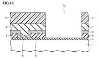
図1に、本発明の光電変換素子の一例である実施の形態1のヘテロ接合型バックコンタクトセルの模式的な断面図を示す。実施の形態1のヘテロ接合型バックコンタクトセルは、n型単結晶シリコンからなる半導体1と、半導体1の裏面の全面を被覆するi型の水素化アモルファスシリコンを含有する真性層4と、真性層4の裏面の一部を被覆するn型の水素化アモルファスシリコンを含有するn型層6と、真性層4の裏面の一部を被覆するp型の水素化アモルファスシリコンを含有するp型層8と、真性層4の裏面の一部を被覆する絶縁層5とを備えている。ここで、n型層6、p型層8および絶縁層5は、互いに、半導体1の裏面の異なる領域を被覆している。
p型層8に含まれるp型不純物としては、たとえばボロンを用いることができ、p型層8のp型不純物濃度は、たとえば5×10¹⁹個/cm3程度とすることができる。
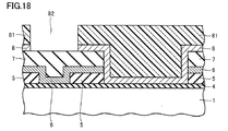
図12に、本発明の光電変換素子の他の一例である実施の形態2のヘテロ接合型バックコンタクトセルの模式的な断面図を示す。実施の形態2のヘテロ接合型バックコンタクトセルにおいては、第1電極9の端部9aがn型層6の裏面上に位置しているとともに、第2電極10の端部10aがp型層8の裏面上に位置していることを特徴としている。
図13に、本発明の光電変換素子のさらに他の一例である実施の形態3のヘテロ接合型バックコンタクトセルの模式的な断面図を示す。実施の形態3のヘテロ接合型バックコンタクトセルにおいては、p型層8の形成後にn型層6を形成していることを特徴としている。
図14に、本発明の光電変換素子のさらに他の一例である実施の形態4のヘテロ接合型バックコンタクトセルの模式的な断面図を示す。実施の形態4のヘテロ接合型バックコンタクトセルは、n型層6の端部6aがp型層8に接していることを特徴としている。
実施の形態5は、実施の形態1〜4のヘテロ接合型バックコンタクトセルを光電変換素子として用いた光電変換モジュールである。
図22に、実施の形態1〜4のヘテロ接合型バックコンタクトセルを光電変換素子として用いた本発明の光電変換モジュールの一例である実施の形態5の光電変換モジュールの構成の概略を示す。図22を参照して、実施の形態5の光電変換モジュール1000は、複数の光電変換素子1001と、カバー1002と、出力端子1013,1014とを備えている。
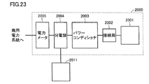
実施の形態6は、実施の形態1〜4のヘテロ接合型バックコンタクトセルを光電変換素子として用いた太陽光発電システムである。
太陽光発電システムは、光電変換モジュールが出力する電力を適宜変換して、商用電力系統または電気機器等に供給する装置である。
実施の形態6の太陽光発電システム2000は、たとえば以下のように動作する。
光電変換モジュールアレイ2001について説明する。
実施の形態7は、実施の形態6として説明した太陽光発電システムよりも大規模な太陽光発電システムである。実施の形態7の太陽光発電システムも、少なくとも1つの実施の形態1〜4のヘテロ接合型バックコンタクトセルを備えるものである。
図25に、本発明の大規模太陽光発電システムの一例である実施の形態7の太陽光発電システムの構成の概略を示す。図25を参照して、実施の形態7の太陽光発電システム4000は、複数のサブシステム4001と、複数のパワーコンディショナ4003と、変圧器4004とを備える。太陽光発電システム4000は、図24に示す実施の形態6の太陽光発電システム2000よりも大規模な太陽光発電システムである。
実施の形態7の太陽光発電システム4000は、たとえば以下のように動作する。

本発明は、半導体と、半導体上に設けられた水素化アモルファスシリコンを含有する真性層と、真性層の一部を被覆する第1導電型の水素化アモルファスシリコンを含有する第1導電型層と、真性層の一部を被覆する第2導電型の水素化アモルファスシリコンを含有する第2導電型層と、第1導電型層の端部領域を被覆する絶縁膜と、第1導電型層上に設けられた第1電極と、第2導電型層上に設けられた第2電極と、を備え、第2導電型層の端部は、絶縁膜上または絶縁膜上方に位置している光電変換素子である。このような構成とすることにより、第2導電型層のパターニングを絶縁膜上で行なうことができ、第2導電型層のパターニング時に、半導体および真性層および第1導電型層が受けるダメージを低減することができる。また、第1導電型層と第2導電型層とが厚さ方向に絶縁されているため、シャント電流を著しく低くすることができる。したがって、本発明の光電変換素子は、高い歩留まりで製造することができ、かつ特性の高い光電変換素子とすることができる。
Claims (8)
- 半導体と、
前記半導体上に設けられた水素化アモルファスシリコンを含有する真性層と、
前記真性層の一部を被覆する、第1導電型の水素化アモルファスシリコンを含有する第1導電型層と、
前記真性層の一部を被覆する、第2導電型の水素化アモルファスシリコンを含有する第2導電型層と、
前記第1導電型層の端部領域を被覆する絶縁膜と、
前記第1導電型層上に設けられた第1電極と、
前記第2導電型層上に設けられた第2電極と、を備え、
前記第2導電型層の端部は、前記絶縁膜上または前記絶縁膜上方に位置し、
前記真性層の一部を被覆する絶縁層をさらに備え、
前記第1導電型層の端部および前記第2導電型層の端部は、前記真性層と前記絶縁層とが接する領域の上方に位置している、光電変換素子。 - 半導体と、
前記半導体上に設けられた水素化アモルファスシリコンを含有する真性層と、
前記真性層の一部を被覆する、第1導電型の水素化アモルファスシリコンを含有する第1導電型層と、
前記真性層の一部を被覆する、第2導電型の水素化アモルファスシリコンを含有する第2導電型層と、
前記第1導電型層の端部領域を被覆する絶縁膜と、
前記第1導電型層上に設けられた第1電極と、
前記第2導電型層上に設けられた第2電極と、を備え、
前記第2導電型層の端部は、前記絶縁膜上または前記絶縁膜上方に位置し、
前記第2導電型層と接する領域における前記真性層の厚さは、前記第1導電型層と接する領域における前記真性層の厚さよりも厚い、光電変換素子。 - 前記第2導電型層と接する領域における前記真性層の厚さは、前記第1導電型層と接する領域における前記真性層の厚さよりも厚い、請求項1に記載の光電変換素子。
- 前記第1電極の端部および前記第2電極の端部が、前記絶縁膜の上方に位置している、請求項1から請求項3のいずれか1項に記載の光電変換素子。
- 前記第2導電型がp型である、請求項1から請求項4のいずれか1項に記載の光電変換素子。
- 前記第2導電型層と前記真性層との間に、第2真性層を有する、請求項1から請求項5のいずれか1項に記載の光電変換素子。
- 請求項1から請求項6のいずれか1項に記載の光電変換素子を複数備える、光電変換モジュール。
- 請求項7に記載の光電変換モジュールを複数備える、太陽光発電システム。
Applications Claiming Priority (3)
| Application Number | Priority Date | Filing Date | Title |
|---|---|---|---|
| JP2013041804 | 2013-03-04 | ||
| JP2013041804 | 2013-03-04 | ||
| PCT/JP2014/055264 WO2014136715A1 (ja) | 2013-03-04 | 2014-03-03 | 光電変換素子 |
Publications (2)
| Publication Number | Publication Date |
|---|---|
| JPWO2014136715A1 JPWO2014136715A1 (ja) | 2017-02-09 |
| JP6360471B2 true JP6360471B2 (ja) | 2018-07-18 |
Family
ID=51491233
Family Applications (1)
| Application Number | Title | Priority Date | Filing Date |
|---|---|---|---|
| JP2015504291A Active JP6360471B2 (ja) | 2013-03-04 | 2014-03-03 | 光電変換素子、光電変換モジュールおよび太陽光発電システム |
Country Status (4)
| Country | Link |
|---|---|
| US (1) | US9806210B2 (ja) |
| JP (1) | JP6360471B2 (ja) |
| CN (1) | CN104995748B (ja) |
| WO (1) | WO2014136715A1 (ja) |
Families Citing this family (9)
| Publication number | Priority date | Publication date | Assignee | Title |
|---|---|---|---|---|
| US9837576B2 (en) * | 2014-09-19 | 2017-12-05 | Sunpower Corporation | Solar cell emitter region fabrication with differentiated P-type and N-type architectures and incorporating dotted diffusion |
| US9559245B2 (en) | 2015-03-23 | 2017-01-31 | Sunpower Corporation | Blister-free polycrystalline silicon for solar cells |
| JP6639295B2 (ja) * | 2016-03-23 | 2020-02-05 | シャープ株式会社 | 光電変換装置、光電変換モジュールおよび太陽光発電システム |
| JP7089473B2 (ja) * | 2016-08-15 | 2022-06-22 | シャープ株式会社 | 光電変換素子および光電変換装置 |
| WO2018168180A1 (ja) * | 2017-03-17 | 2018-09-20 | 株式会社カネカ | 太陽電池およびその製造方法 |
| US11682744B2 (en) * | 2018-09-28 | 2023-06-20 | Maxeon Solar Pte. Ltd. | Solar cells having hybrid architectures including differentiated P-type and N-type regions |
| CN111477694A (zh) * | 2019-01-23 | 2020-07-31 | 福建金石能源有限公司 | 一种背接触异质结太阳能电池及其制作方法 |
| WO2021010422A1 (ja) * | 2019-07-16 | 2021-01-21 | 株式会社カネカ | 太陽電池および太陽電池の製造方法 |
| CN112133774A (zh) * | 2020-10-12 | 2020-12-25 | 青海黄河上游水电开发有限责任公司光伏产业技术分公司 | 一种背结背接触太阳能电池及其制作方法 |
Family Cites Families (11)
| Publication number | Priority date | Publication date | Assignee | Title |
|---|---|---|---|---|
| US4415760A (en) * | 1982-04-12 | 1983-11-15 | Chevron Research Company | Amorphous silicon solar cells incorporating an insulating layer in the body of amorphous silicon and a method of suppressing the back diffusion of holes into an N-type region |
| US7339110B1 (en) * | 2003-04-10 | 2008-03-04 | Sunpower Corporation | Solar cell and method of manufacture |
| US20070169808A1 (en) | 2006-01-26 | 2007-07-26 | Kherani Nazir P | Solar cell |
| JP2009152222A (ja) * | 2006-10-27 | 2009-07-09 | Kyocera Corp | 太陽電池素子の製造方法 |
| US20110000532A1 (en) | 2008-01-30 | 2011-01-06 | Kyocera Corporation | Solar Cell Device and Method of Manufacturing Solar Cell Device |
| US8220210B2 (en) | 2008-06-27 | 2012-07-17 | Sunpower Corporation | Photovoltaic module and module arrays |
| SG175041A1 (en) * | 2009-03-30 | 2011-11-28 | Sanyo Electric Co | Solar cell |
| CN102725858B (zh) | 2010-01-26 | 2015-12-09 | 三洋电机株式会社 | 太阳能电池及其制造方法 |
| JP5906393B2 (ja) * | 2010-02-26 | 2016-04-20 | パナソニックIpマネジメント株式会社 | 太陽電池及び太陽電池の製造方法 |
| KR101275575B1 (ko) * | 2010-10-11 | 2013-06-14 | 엘지전자 주식회사 | 후면전극형 태양전지 및 이의 제조 방법 |
| GB2503513A (en) * | 2012-06-29 | 2014-01-01 | Rec Cells Pte Ltd | A rear contact heterojunction intrinsic thin layer silicon solar cell |
-
2014
- 2014-03-03 JP JP2015504291A patent/JP6360471B2/ja active Active
- 2014-03-03 WO PCT/JP2014/055264 patent/WO2014136715A1/ja active Application Filing
- 2014-03-03 CN CN201480008353.4A patent/CN104995748B/zh active Active
- 2014-03-03 US US14/762,880 patent/US9806210B2/en active Active
Also Published As
| Publication number | Publication date |
|---|---|
| CN104995748B (zh) | 2017-03-08 |
| WO2014136715A1 (ja) | 2014-09-12 |
| US9806210B2 (en) | 2017-10-31 |
| CN104995748A (zh) | 2015-10-21 |
| US20150372172A1 (en) | 2015-12-24 |
| JPWO2014136715A1 (ja) | 2017-02-09 |
Similar Documents
| Publication | Publication Date | Title |
|---|---|---|
| JP6360471B2 (ja) | 光電変換素子、光電変換モジュールおよび太陽光発電システム | |
| US20170194516A1 (en) | Advanced design of metallic grid in photovoltaic structures | |
| US8877545B2 (en) | Method of manufacturing solar cell | |
| JP6284522B2 (ja) | 光電変換素子、光電変換モジュールおよび太陽光発電システム | |
| JP2015225900A (ja) | 太陽電池の製造方法及び太陽電池 | |
| JP2014075526A (ja) | 光電変換素子および光電変換素子の製造方法 | |
| JP6223424B2 (ja) | 光電変換素子 | |
| US20080241356A1 (en) | Photovoltaic devices manufactured using crystalline silicon thin films on glass | |
| US9997647B2 (en) | Solar cells and manufacturing method thereof | |
| EP2903037A1 (en) | Fabrication method for back-contact heterojunction solar cell | |
| NL2034302B1 (en) | Solar cell and photovoltaic module | |
| US20130092224A1 (en) | Photoelectric device | |
| US9780241B2 (en) | Solar cell | |
| JPWO2012017517A1 (ja) | 太陽電池セル | |
| WO2014163043A1 (ja) | 光電変換素子 | |
| WO2012090650A1 (ja) | 太陽電池 | |
| KR20120129016A (ko) | 양면 수광형 국부화 에미터 태양전지 | |
| US10505055B2 (en) | Photoelectric conversion element | |
| JP6198813B2 (ja) | 光電変換素子、光電変換モジュールおよび太陽光発電システム | |
| JP2014056875A (ja) | 光電変換素子および光電変換素子の製造方法 | |
| JP2014072210A (ja) | 光電変換素子 | |
| KR20160147101A (ko) | 박막형 태양전지와 그의 제조방법 | |
| JP2016063071A (ja) | 光電変換素子および光電変換素子の製造方法 |
Legal Events
| Date | Code | Title | Description |
|---|---|---|---|
| A131 | Notification of reasons for refusal |
Free format text: JAPANESE INTERMEDIATE CODE: A131 Effective date: 20170606 |
|
| A521 | Written amendment |
Free format text: JAPANESE INTERMEDIATE CODE: A523 Effective date: 20170803 |
|
| A02 | Decision of refusal |
Free format text: JAPANESE INTERMEDIATE CODE: A02 Effective date: 20180109 |
|
| A521 | Written amendment |
Free format text: JAPANESE INTERMEDIATE CODE: A523 Effective date: 20180330 |
|
| A911 | Transfer of reconsideration by examiner before appeal (zenchi) |
Free format text: JAPANESE INTERMEDIATE CODE: A911 Effective date: 20180416 |
|
| TRDD | Decision of grant or rejection written | ||
| A01 | Written decision to grant a patent or to grant a registration (utility model) |
Free format text: JAPANESE INTERMEDIATE CODE: A01 Effective date: 20180529 |
|
| A61 | First payment of annual fees (during grant procedure) |
Free format text: JAPANESE INTERMEDIATE CODE: A61 Effective date: 20180622 |
|
| R150 | Certificate of patent or registration of utility model |
Ref document number: 6360471 Country of ref document: JP Free format text: JAPANESE INTERMEDIATE CODE: R150 |