JP6284522B2 - 光電変換素子、光電変換モジュールおよび太陽光発電システム - Google Patents
光電変換素子、光電変換モジュールおよび太陽光発電システム Download PDFInfo
- Publication number
- JP6284522B2 JP6284522B2 JP2015508697A JP2015508697A JP6284522B2 JP 6284522 B2 JP6284522 B2 JP 6284522B2 JP 2015508697 A JP2015508697 A JP 2015508697A JP 2015508697 A JP2015508697 A JP 2015508697A JP 6284522 B2 JP6284522 B2 JP 6284522B2
- Authority
- JP
- Japan
- Prior art keywords
- layer
- photoelectric conversion
- type layer
- electrode
- conductivity type
- Prior art date
- Legal status (The legal status is an assumption and is not a legal conclusion. Google has not performed a legal analysis and makes no representation as to the accuracy of the status listed.)
- Active
Links
- 238000006243 chemical reaction Methods 0.000 title claims description 99
- 238000010248 power generation Methods 0.000 title claims description 43
- 239000004065 semiconductor Substances 0.000 claims description 51
- 229910021417 amorphous silicon Inorganic materials 0.000 claims description 39
- 229910044991 metal oxide Inorganic materials 0.000 claims description 2
- 150000004706 metal oxides Chemical class 0.000 claims description 2
- 238000000034 method Methods 0.000 description 41
- KRHYYFGTRYWZRS-UHFFFAOYSA-N Fluorane Chemical compound F KRHYYFGTRYWZRS-UHFFFAOYSA-N 0.000 description 30
- 238000004519 manufacturing process Methods 0.000 description 26
- 238000005530 etching Methods 0.000 description 18
- 238000001039 wet etching Methods 0.000 description 16
- 238000005268 plasma chemical vapour deposition Methods 0.000 description 15
- 238000003860 storage Methods 0.000 description 14
- HEMHJVSKTPXQMS-UHFFFAOYSA-M Sodium hydroxide Chemical compound [OH-].[Na+] HEMHJVSKTPXQMS-UHFFFAOYSA-M 0.000 description 12
- 238000009826 distribution Methods 0.000 description 12
- 229910052581 Si3N4 Inorganic materials 0.000 description 11
- VYPSYNLAJGMNEJ-UHFFFAOYSA-N Silicium dioxide Chemical compound O=[Si]=O VYPSYNLAJGMNEJ-UHFFFAOYSA-N 0.000 description 11
- HQVNEWCFYHHQES-UHFFFAOYSA-N silicon nitride Chemical compound N12[Si]34N5[Si]62N3[Si]51N64 HQVNEWCFYHHQES-UHFFFAOYSA-N 0.000 description 11
- 229910052814 silicon oxide Inorganic materials 0.000 description 11
- 239000007864 aqueous solution Substances 0.000 description 10
- 238000000059 patterning Methods 0.000 description 9
- WGTYBPLFGIVFAS-UHFFFAOYSA-M tetramethylammonium hydroxide Chemical compound [OH-].C[N+](C)(C)C WGTYBPLFGIVFAS-UHFFFAOYSA-M 0.000 description 8
- 230000007704 transition Effects 0.000 description 8
- KWYUFKZDYYNOTN-UHFFFAOYSA-M Potassium hydroxide Chemical compound [OH-].[K+] KWYUFKZDYYNOTN-UHFFFAOYSA-M 0.000 description 6
- 229910021419 crystalline silicon Inorganic materials 0.000 description 6
- 238000002161 passivation Methods 0.000 description 6
- 239000000243 solution Substances 0.000 description 6
- 230000008569 process Effects 0.000 description 5
- VEXZGXHMUGYJMC-UHFFFAOYSA-N Hydrochloric acid Chemical compound Cl VEXZGXHMUGYJMC-UHFFFAOYSA-N 0.000 description 4
- BQCADISMDOOEFD-UHFFFAOYSA-N Silver Chemical compound [Ag] BQCADISMDOOEFD-UHFFFAOYSA-N 0.000 description 4
- 239000012535 impurity Substances 0.000 description 4
- 238000000206 photolithography Methods 0.000 description 4
- 229910052709 silver Inorganic materials 0.000 description 4
- 239000004332 silver Substances 0.000 description 4
- 229910052782 aluminium Inorganic materials 0.000 description 3
- XAGFODPZIPBFFR-UHFFFAOYSA-N aluminium Chemical compound [Al] XAGFODPZIPBFFR-UHFFFAOYSA-N 0.000 description 3
- 230000000694 effects Effects 0.000 description 3
- 239000000463 material Substances 0.000 description 3
- 238000007740 vapor deposition Methods 0.000 description 3
- 238000003491 array Methods 0.000 description 2
- 238000010586 diagram Methods 0.000 description 2
- 230000005611 electricity Effects 0.000 description 2
- 238000003475 lamination Methods 0.000 description 2
- 238000001459 lithography Methods 0.000 description 2
- 230000000873 masking effect Effects 0.000 description 2
- 229910052751 metal Inorganic materials 0.000 description 2
- 239000002184 metal Substances 0.000 description 2
- 238000012544 monitoring process Methods 0.000 description 2
- 229910021421 monocrystalline silicon Inorganic materials 0.000 description 2
- 239000012466 permeate Substances 0.000 description 2
- 238000004544 sputter deposition Methods 0.000 description 2
- ZOXJGFHDIHLPTG-UHFFFAOYSA-N Boron Chemical compound [B] ZOXJGFHDIHLPTG-UHFFFAOYSA-N 0.000 description 1
- OAICVXFJPJFONN-UHFFFAOYSA-N Phosphorus Chemical compound [P] OAICVXFJPJFONN-UHFFFAOYSA-N 0.000 description 1
- XUIMIQQOPSSXEZ-UHFFFAOYSA-N Silicon Chemical compound [Si] XUIMIQQOPSSXEZ-UHFFFAOYSA-N 0.000 description 1
- 238000000137 annealing Methods 0.000 description 1
- 230000008901 benefit Effects 0.000 description 1
- 230000015572 biosynthetic process Effects 0.000 description 1
- 229910052796 boron Inorganic materials 0.000 description 1
- 238000005229 chemical vapour deposition Methods 0.000 description 1
- 238000004140 cleaning Methods 0.000 description 1
- 239000011248 coating agent Substances 0.000 description 1
- 238000000576 coating method Methods 0.000 description 1
- 150000001875 compounds Chemical class 0.000 description 1
- 239000004020 conductor Substances 0.000 description 1
- 239000013078 crystal Substances 0.000 description 1
- 238000005265 energy consumption Methods 0.000 description 1
- 230000007613 environmental effect Effects 0.000 description 1
- AMGQUBHHOARCQH-UHFFFAOYSA-N indium;oxotin Chemical compound [In].[Sn]=O AMGQUBHHOARCQH-UHFFFAOYSA-N 0.000 description 1
- 239000011810 insulating material Substances 0.000 description 1
- 238000012986 modification Methods 0.000 description 1
- 230000004048 modification Effects 0.000 description 1
- 239000011368 organic material Substances 0.000 description 1
- 239000011574 phosphorus Substances 0.000 description 1
- 229910052698 phosphorus Inorganic materials 0.000 description 1
- 230000035945 sensitivity Effects 0.000 description 1
- 238000000926 separation method Methods 0.000 description 1
- 229910052710 silicon Inorganic materials 0.000 description 1
- 239000010703 silicon Substances 0.000 description 1
Images


Classifications
-
- H—ELECTRICITY
- H01—ELECTRIC ELEMENTS
- H01L—SEMICONDUCTOR DEVICES NOT COVERED BY CLASS H10
- H01L31/00—Semiconductor devices sensitive to infrared radiation, light, electromagnetic radiation of shorter wavelength or corpuscular radiation and specially adapted either for the conversion of the energy of such radiation into electrical energy or for the control of electrical energy by such radiation; Processes or apparatus specially adapted for the manufacture or treatment thereof or of parts thereof; Details thereof
- H01L31/02—Details
- H01L31/0224—Electrodes
- H01L31/022408—Electrodes for devices characterised by at least one potential jump barrier or surface barrier
- H01L31/022425—Electrodes for devices characterised by at least one potential jump barrier or surface barrier for solar cells
- H01L31/022433—Particular geometry of the grid contacts
-
- H—ELECTRICITY
- H01—ELECTRIC ELEMENTS
- H01L—SEMICONDUCTOR DEVICES NOT COVERED BY CLASS H10
- H01L31/00—Semiconductor devices sensitive to infrared radiation, light, electromagnetic radiation of shorter wavelength or corpuscular radiation and specially adapted either for the conversion of the energy of such radiation into electrical energy or for the control of electrical energy by such radiation; Processes or apparatus specially adapted for the manufacture or treatment thereof or of parts thereof; Details thereof
- H01L31/0248—Semiconductor devices sensitive to infrared radiation, light, electromagnetic radiation of shorter wavelength or corpuscular radiation and specially adapted either for the conversion of the energy of such radiation into electrical energy or for the control of electrical energy by such radiation; Processes or apparatus specially adapted for the manufacture or treatment thereof or of parts thereof; Details thereof characterised by their semiconductor bodies
- H01L31/036—Semiconductor devices sensitive to infrared radiation, light, electromagnetic radiation of shorter wavelength or corpuscular radiation and specially adapted either for the conversion of the energy of such radiation into electrical energy or for the control of electrical energy by such radiation; Processes or apparatus specially adapted for the manufacture or treatment thereof or of parts thereof; Details thereof characterised by their semiconductor bodies characterised by their crystalline structure or particular orientation of the crystalline planes
- H01L31/0376—Semiconductor devices sensitive to infrared radiation, light, electromagnetic radiation of shorter wavelength or corpuscular radiation and specially adapted either for the conversion of the energy of such radiation into electrical energy or for the control of electrical energy by such radiation; Processes or apparatus specially adapted for the manufacture or treatment thereof or of parts thereof; Details thereof characterised by their semiconductor bodies characterised by their crystalline structure or particular orientation of the crystalline planes including amorphous semiconductors
- H01L31/03762—Semiconductor devices sensitive to infrared radiation, light, electromagnetic radiation of shorter wavelength or corpuscular radiation and specially adapted either for the conversion of the energy of such radiation into electrical energy or for the control of electrical energy by such radiation; Processes or apparatus specially adapted for the manufacture or treatment thereof or of parts thereof; Details thereof characterised by their semiconductor bodies characterised by their crystalline structure or particular orientation of the crystalline planes including amorphous semiconductors including only elements of Group IV of the Periodic System
-
- H—ELECTRICITY
- H01—ELECTRIC ELEMENTS
- H01L—SEMICONDUCTOR DEVICES NOT COVERED BY CLASS H10
- H01L31/00—Semiconductor devices sensitive to infrared radiation, light, electromagnetic radiation of shorter wavelength or corpuscular radiation and specially adapted either for the conversion of the energy of such radiation into electrical energy or for the control of electrical energy by such radiation; Processes or apparatus specially adapted for the manufacture or treatment thereof or of parts thereof; Details thereof
- H01L31/04—Semiconductor devices sensitive to infrared radiation, light, electromagnetic radiation of shorter wavelength or corpuscular radiation and specially adapted either for the conversion of the energy of such radiation into electrical energy or for the control of electrical energy by such radiation; Processes or apparatus specially adapted for the manufacture or treatment thereof or of parts thereof; Details thereof adapted as photovoltaic [PV] conversion devices
- H01L31/06—Semiconductor devices sensitive to infrared radiation, light, electromagnetic radiation of shorter wavelength or corpuscular radiation and specially adapted either for the conversion of the energy of such radiation into electrical energy or for the control of electrical energy by such radiation; Processes or apparatus specially adapted for the manufacture or treatment thereof or of parts thereof; Details thereof adapted as photovoltaic [PV] conversion devices characterised by at least one potential-jump barrier or surface barrier
- H01L31/072—Semiconductor devices sensitive to infrared radiation, light, electromagnetic radiation of shorter wavelength or corpuscular radiation and specially adapted either for the conversion of the energy of such radiation into electrical energy or for the control of electrical energy by such radiation; Processes or apparatus specially adapted for the manufacture or treatment thereof or of parts thereof; Details thereof adapted as photovoltaic [PV] conversion devices characterised by at least one potential-jump barrier or surface barrier the potential barriers being only of the PN heterojunction type
- H01L31/0745—Semiconductor devices sensitive to infrared radiation, light, electromagnetic radiation of shorter wavelength or corpuscular radiation and specially adapted either for the conversion of the energy of such radiation into electrical energy or for the control of electrical energy by such radiation; Processes or apparatus specially adapted for the manufacture or treatment thereof or of parts thereof; Details thereof adapted as photovoltaic [PV] conversion devices characterised by at least one potential-jump barrier or surface barrier the potential barriers being only of the PN heterojunction type comprising a AIVBIV heterojunction, e.g. Si/Ge, SiGe/Si or Si/SiC solar cells
- H01L31/0747—Semiconductor devices sensitive to infrared radiation, light, electromagnetic radiation of shorter wavelength or corpuscular radiation and specially adapted either for the conversion of the energy of such radiation into electrical energy or for the control of electrical energy by such radiation; Processes or apparatus specially adapted for the manufacture or treatment thereof or of parts thereof; Details thereof adapted as photovoltaic [PV] conversion devices characterised by at least one potential-jump barrier or surface barrier the potential barriers being only of the PN heterojunction type comprising a AIVBIV heterojunction, e.g. Si/Ge, SiGe/Si or Si/SiC solar cells comprising a heterojunction of crystalline and amorphous materials, e.g. heterojunction with intrinsic thin layer or HIT® solar cells; solar cells
-
- H—ELECTRICITY
- H01—ELECTRIC ELEMENTS
- H01L—SEMICONDUCTOR DEVICES NOT COVERED BY CLASS H10
- H01L31/00—Semiconductor devices sensitive to infrared radiation, light, electromagnetic radiation of shorter wavelength or corpuscular radiation and specially adapted either for the conversion of the energy of such radiation into electrical energy or for the control of electrical energy by such radiation; Processes or apparatus specially adapted for the manufacture or treatment thereof or of parts thereof; Details thereof
- H01L31/04—Semiconductor devices sensitive to infrared radiation, light, electromagnetic radiation of shorter wavelength or corpuscular radiation and specially adapted either for the conversion of the energy of such radiation into electrical energy or for the control of electrical energy by such radiation; Processes or apparatus specially adapted for the manufacture or treatment thereof or of parts thereof; Details thereof adapted as photovoltaic [PV] conversion devices
- H01L31/06—Semiconductor devices sensitive to infrared radiation, light, electromagnetic radiation of shorter wavelength or corpuscular radiation and specially adapted either for the conversion of the energy of such radiation into electrical energy or for the control of electrical energy by such radiation; Processes or apparatus specially adapted for the manufacture or treatment thereof or of parts thereof; Details thereof adapted as photovoltaic [PV] conversion devices characterised by at least one potential-jump barrier or surface barrier
- H01L31/075—Semiconductor devices sensitive to infrared radiation, light, electromagnetic radiation of shorter wavelength or corpuscular radiation and specially adapted either for the conversion of the energy of such radiation into electrical energy or for the control of electrical energy by such radiation; Processes or apparatus specially adapted for the manufacture or treatment thereof or of parts thereof; Details thereof adapted as photovoltaic [PV] conversion devices characterised by at least one potential-jump barrier or surface barrier the potential barriers being only of the PIN type
-
- Y—GENERAL TAGGING OF NEW TECHNOLOGICAL DEVELOPMENTS; GENERAL TAGGING OF CROSS-SECTIONAL TECHNOLOGIES SPANNING OVER SEVERAL SECTIONS OF THE IPC; TECHNICAL SUBJECTS COVERED BY FORMER USPC CROSS-REFERENCE ART COLLECTIONS [XRACs] AND DIGESTS
- Y02—TECHNOLOGIES OR APPLICATIONS FOR MITIGATION OR ADAPTATION AGAINST CLIMATE CHANGE
- Y02E—REDUCTION OF GREENHOUSE GAS [GHG] EMISSIONS, RELATED TO ENERGY GENERATION, TRANSMISSION OR DISTRIBUTION
- Y02E10/00—Energy generation through renewable energy sources
- Y02E10/50—Photovoltaic [PV] energy
- Y02E10/548—Amorphous silicon PV cells
Landscapes
- Engineering & Computer Science (AREA)
- Microelectronics & Electronic Packaging (AREA)
- Electromagnetism (AREA)
- General Physics & Mathematics (AREA)
- Condensed Matter Physics & Semiconductors (AREA)
- Computer Hardware Design (AREA)
- Physics & Mathematics (AREA)
- Power Engineering (AREA)
- Life Sciences & Earth Sciences (AREA)
- Sustainable Energy (AREA)
- Sustainable Development (AREA)
- Chemical & Material Sciences (AREA)
- Crystallography & Structural Chemistry (AREA)
- Photovoltaic Devices (AREA)
Description
図1に、本発明の光電変換素子の一例である実施の形態1のヘテロ接合型バックコンタクトセルの模式的な断面図を示す。実施の形態1のヘテロ接合型バックコンタクトセルは、n型単結晶シリコンからなる半導体1と、半導体1の裏面の全面を被覆するi型の水素化アモルファスシリコンを含有する真性層2と、真性層2の裏面の一部を被覆するn型の水素化アモルファスシリコンを含有するn型層4と、真性層2の裏面の一部を被覆するp型の水素化アモルファスシリコンを含有するp型層5と、真性層2の裏面の一部を被覆する絶縁層3とを備えている。ここで、n型層4、p型層5および絶縁層3は、互いに、半導体1の裏面の異なる領域を被覆している。
図8に、本発明の光電変換素子の他の一例である実施の形態2のヘテロ接合型バックコンタクトセルの模式的な断面図を示す。実施の形態2のヘテロ接合型バックコンタクトセルは、n型層4の端部4aがp型層5に接していることを特徴としている。
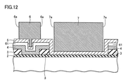
図12に、本発明の光電変換素子の他の一例である実施の形態3のヘテロ接合型バックコンタクトセルの模式的な断面図を示す。実施の形態3のヘテロ接合型バックコンタクトセルは、n型層4とp型層5との間に中間層61が配置されていることを特徴としている。
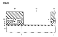
図16に、本発明の光電変換素子の他の一例である実施の形態4のヘテロ接合型バックコンタクトセルの模式的な断面図を示す。実施の形態4のヘテロ接合型バックコンタクトセルは、n型層4とp型層5との間の中間層61の端部61aが絶縁層3上に位置していることを特徴としている。
実施の形態5は、実施の形態1〜4のヘテロ接合型バックコンタクトセルを光電変換素子として用いた光電変換モジュールである。
図22に、実施の形態1〜4のヘテロ接合型バックコンタクトセルを光電変換素子として用いた本発明の光電変換モジュールの一例である実施の形態5の光電変換モジュールの構成の概略を示す。図22を参照して、実施の形態5の光電変換モジュール1000は、複数の光電変換素子1001と、カバー1002と、出力端子1013,1014とを備えている。
実施の形態6は、実施の形態1〜4のヘテロ接合型バックコンタクトセルを光電変換素子として用いた太陽光発電システムである。本発明の光電変換素子は高い特性(変換効率等)を有するため、これを備える本発明の太陽光発電システムも高い特性を有することができる。尚、太陽光発電システムとは、光電変換モジュールが出力する電力を適宜変換して、商用電力系統または電気機器等に供給する装置である。
太陽光発電システムは、光電変換モジュールが出力する電力を適宜変換して、商用電力系統または電気機器等に供給する装置である。
実施の形態6の太陽光発電システム2000は、たとえば以下のように動作する。
光電変換モジュールアレイ2001について説明する。
実施の形態7は、実施の形態6として説明した太陽光発電システムよりも大規模な太陽光発電システムである。実施の形態7の太陽光発電システムも、少なくとも1つの実施の形態1〜4のヘテロ接合型バックコンタクトセルを備えるものである。本発明の光電変換素子は高い特性(変換効率等)を有するため、これを備える本発明の太陽光発電システムも高い特性を有することができる。
図25に、本発明の大規模太陽光発電システムの一例である実施の形態7の太陽光発電システムの構成の概略を示す。図25を参照して、実施の形態7の太陽光発電システム4000は、複数のサブシステム4001と、複数のパワーコンディショナ4003と、変圧器4004とを備える。太陽光発電システム4000は、図24に示す実施の形態6の太陽光発電システム2000よりも大規模な太陽光発電システムである。
実施の形態7の太陽光発電システム4000は、たとえば以下のように動作する。

Claims (11)
- 第1導電型の半導体と、
前記半導体上に設けられた水素化アモルファスシリコンを含有する真性層と、
前記真性層の一部を被覆する、第1導電型の水素化アモルファスシリコンを含有する第1導電型層と、
前記真性層の一部を被覆する、第2導電型の水素化アモルファスシリコンを含有する第2導電型層と、
前記真性層の前記半導体とは反対側の面に接する絶縁層と、
前記第2導電型層上に設けられた第1電極と、
前記第2導電型層上に設けられた第2電極と、を備え、
前記第1電極は、前記第2導電型層を介して、前記第1導電型層と前記第2導電型層との接合領域の上に設けられているとともに、
前記第1電極の少なくとも一部が、前記第1導電型層と前記真性層とが接する領域の上方に位置しており、
前記第2電極の少なくとも一部が、前記第2導電型層と前記真性層とが接する領域の上方に位置している、光電変換素子。 - 前記第2導電型層は、少なくとも、前記第2導電型層と前記第1電極とが接する領域から、前記第2導電型層と前記第2電極とが接する領域にわたって設けられ、
前記第2導電型層は、前記絶縁層の一部と接する、請求項1に記載の光電変換素子。 - 前記第1導電型層の端部が、前記絶縁層上に位置している、請求項1または2に記載の光電変換素子。
- 前記第1電極の端部および前記第2電極の端部が、前記絶縁層の上方に位置している、請求項1から3のいずれか1項に記載の光電変換素子。
- 前記第2導電型がp型である、請求項1から4のいずれか1項に記載の光電変換素子。
- 第1導電型の半導体と、
前記半導体上に設けられた水素化アモルファスシリコンを含有する真性層と、
前記真性層の一部を被覆する、第1導電型の水素化アモルファスシリコンを含有する第1導電型層と、
前記真性層の一部を被覆する、第2導電型の水素化アモルファスシリコンを含有する第2導電型層と、
前記真性層の前記半導体とは反対側の面に接する絶縁層と、
前記第1導電型層上に設けられた中間層と、
前記第2導電型層上に設けられた第1電極と、
前記第2導電型層上に設けられた第2電極と、を備え、
前記第1電極は、前記半導体と前記真性層とが接し、且つ、前記真性層と前記第1導電型層とが接し、且つ、前記第1導電型層と前記中間層とが接し、且つ、前記中間層と前記第2導電型層とが接する領域上に設けられた、光電変換素子。 - 前記中間層は、金属酸化物からなる、請求項6に記載の光電変換素子。
- 前記中間層は、ITOまたはIZOのいずれか1つを含む、請求項6または7に記載の光電変換素子。
- 前記中間層の端部は、前記絶縁層上方に位置する、請求項6から8のいずれか1項に記載の光電変換素子。
- 請求項1から9のいずれか1項に記載の光電変換素子を複数備える、光電変換モジュール。
- 請求項10に記載の光電変換モジュールを複数備える、太陽光発電システム。
Applications Claiming Priority (3)
| Application Number | Priority Date | Filing Date | Title |
|---|---|---|---|
| JP2013069746 | 2013-03-28 | ||
| JP2013069746 | 2013-03-28 | ||
| PCT/JP2014/058870 WO2014157521A1 (ja) | 2013-03-28 | 2014-03-27 | 光電変換素子 |
Publications (2)
| Publication Number | Publication Date |
|---|---|
| JPWO2014157521A1 JPWO2014157521A1 (ja) | 2017-02-16 |
| JP6284522B2 true JP6284522B2 (ja) | 2018-02-28 |
Family
ID=51624482
Family Applications (1)
| Application Number | Title | Priority Date | Filing Date |
|---|---|---|---|
| JP2015508697A Active JP6284522B2 (ja) | 2013-03-28 | 2014-03-27 | 光電変換素子、光電変換モジュールおよび太陽光発電システム |
Country Status (4)
| Country | Link |
|---|---|
| US (1) | US9761743B2 (ja) |
| JP (1) | JP6284522B2 (ja) |
| CN (1) | CN104995747B (ja) |
| WO (1) | WO2014157521A1 (ja) |
Families Citing this family (6)
| Publication number | Priority date | Publication date | Assignee | Title |
|---|---|---|---|---|
| JP6697824B2 (ja) * | 2015-01-14 | 2020-05-27 | シャープ株式会社 | 光電変換素子、それを備えた太陽電池モジュールおよび太陽光発電システム |
| EP3223318A1 (en) * | 2016-03-23 | 2017-09-27 | Meyer Burger (Germany) AG | Hetero junction photovoltaic cell and method of manufacturing same |
| CN110047965A (zh) * | 2018-01-16 | 2019-07-23 | 福建金石能源有限公司 | 一种新型的背接触异质结电池及其制作方法 |
| CN114365294B (zh) * | 2019-07-16 | 2024-03-26 | 株式会社钟化 | 太阳能电池和太阳能电池的制造方法 |
| CN114496737A (zh) * | 2020-11-12 | 2022-05-13 | 长鑫存储技术有限公司 | 半导体器件及其制造方法 |
| TWI816357B (zh) * | 2022-04-08 | 2023-09-21 | 長庚大學 | 太陽能電池模組及其製備方法 |
Family Cites Families (12)
| Publication number | Priority date | Publication date | Assignee | Title |
|---|---|---|---|---|
| JP2002359310A (ja) * | 2001-05-30 | 2002-12-13 | Matsushita Electric Ind Co Ltd | 半導体装置、及びその製造方法 |
| JP3998619B2 (ja) * | 2003-09-24 | 2007-10-31 | 三洋電機株式会社 | 光起電力素子およびその製造方法 |
| CN100431177C (zh) | 2003-09-24 | 2008-11-05 | 三洋电机株式会社 | 光生伏打元件及其制造方法 |
| US20070169808A1 (en) | 2006-01-26 | 2007-07-26 | Kherani Nazir P | Solar cell |
| JP5230222B2 (ja) * | 2008-02-21 | 2013-07-10 | 三洋電機株式会社 | 太陽電池 |
| JP5461028B2 (ja) * | 2009-02-26 | 2014-04-02 | 三洋電機株式会社 | 太陽電池 |
| EP2408021A4 (en) * | 2009-03-10 | 2017-05-17 | Panasonic Intellectual Property Management Co., Ltd. | Process for producing solar battery, and solar battery |
| WO2010113750A1 (ja) * | 2009-03-30 | 2010-10-07 | 三洋電機株式会社 | 太陽電池 |
| CN102725858B (zh) * | 2010-01-26 | 2015-12-09 | 三洋电机株式会社 | 太阳能电池及其制造方法 |
| EP2541617B1 (en) * | 2010-02-26 | 2017-03-22 | Panasonic Intellectual Property Management Co., Ltd. | Solar cell and method for manufacturing solar cell |
| JP2013219065A (ja) * | 2010-08-06 | 2013-10-24 | Sanyo Electric Co Ltd | 太陽電池及び太陽電池の製造方法 |
| GB2503513A (en) * | 2012-06-29 | 2014-01-01 | Rec Cells Pte Ltd | A rear contact heterojunction intrinsic thin layer silicon solar cell |
-
2014
- 2014-03-27 CN CN201480008279.6A patent/CN104995747B/zh active Active
- 2014-03-27 WO PCT/JP2014/058870 patent/WO2014157521A1/ja active Application Filing
- 2014-03-27 US US14/764,224 patent/US9761743B2/en active Active
- 2014-03-27 JP JP2015508697A patent/JP6284522B2/ja active Active
Also Published As
| Publication number | Publication date |
|---|---|
| US9761743B2 (en) | 2017-09-12 |
| US20150364624A1 (en) | 2015-12-17 |
| JPWO2014157521A1 (ja) | 2017-02-16 |
| CN104995747B (zh) | 2016-12-14 |
| CN104995747A (zh) | 2015-10-21 |
| WO2014157521A1 (ja) | 2014-10-02 |
Similar Documents
| Publication | Publication Date | Title |
|---|---|---|
| JP6360471B2 (ja) | 光電変換素子、光電変換モジュールおよび太陽光発電システム | |
| JP6284522B2 (ja) | 光電変換素子、光電変換モジュールおよび太陽光発電システム | |
| JP5347409B2 (ja) | 太陽電池及びその製造方法 | |
| JP6350858B2 (ja) | 太陽電池の製造方法及び太陽電池 | |
| JP5334926B2 (ja) | 太陽電池の製造方法 | |
| JP2014075526A (ja) | 光電変換素子および光電変換素子の製造方法 | |
| JP6223424B2 (ja) | 光電変換素子 | |
| US9997647B2 (en) | Solar cells and manufacturing method thereof | |
| US10658526B2 (en) | Photovoltaic device | |
| US20130092224A1 (en) | Photoelectric device | |
| US9780241B2 (en) | Solar cell | |
| WO2014163043A1 (ja) | 光電変換素子 | |
| US10505055B2 (en) | Photoelectric conversion element | |
| KR20120077712A (ko) | 양면 수광형 국부화 에미터 태양전지 및 그 제조 방법 | |
| JP6198813B2 (ja) | 光電変換素子、光電変換モジュールおよび太陽光発電システム | |
| JP2014183073A (ja) | 光電変換素子および光電変換素子の製造方法 | |
| JP2014056875A (ja) | 光電変換素子および光電変換素子の製造方法 | |
| JP2014072210A (ja) | 光電変換素子 | |
| KR20160147101A (ko) | 박막형 태양전지와 그의 제조방법 |
Legal Events
| Date | Code | Title | Description |
|---|---|---|---|
| A131 | Notification of reasons for refusal |
Free format text: JAPANESE INTERMEDIATE CODE: A131 Effective date: 20170606 |
|
| A521 | Written amendment |
Free format text: JAPANESE INTERMEDIATE CODE: A523 Effective date: 20170803 |
|
| TRDD | Decision of grant or rejection written | ||
| A01 | Written decision to grant a patent or to grant a registration (utility model) |
Free format text: JAPANESE INTERMEDIATE CODE: A01 Effective date: 20180109 |
|
| A61 | First payment of annual fees (during grant procedure) |
Free format text: JAPANESE INTERMEDIATE CODE: A61 Effective date: 20180130 |
|
| R150 | Certificate of patent or registration of utility model |
Ref document number: 6284522 Country of ref document: JP Free format text: JAPANESE INTERMEDIATE CODE: R150 |