JP6336294B2 - スイッチング電源システムに使用される制御装置 - Google Patents
スイッチング電源システムに使用される制御装置 Download PDFInfo
- Publication number
- JP6336294B2 JP6336294B2 JP2014033000A JP2014033000A JP6336294B2 JP 6336294 B2 JP6336294 B2 JP 6336294B2 JP 2014033000 A JP2014033000 A JP 2014033000A JP 2014033000 A JP2014033000 A JP 2014033000A JP 6336294 B2 JP6336294 B2 JP 6336294B2
- Authority
- JP
- Japan
- Prior art keywords
- transistor
- power supply
- gate
- capacitor
- supply system
- Prior art date
- Legal status (The legal status is an assumption and is not a legal conclusion. Google has not performed a legal analysis and makes no representation as to the accuracy of the status listed.)
- Active
Links
- 239000003990 capacitor Substances 0.000 claims description 40
- 230000008878 coupling Effects 0.000 description 4
- 238000010168 coupling process Methods 0.000 description 4
- 238000005859 coupling reaction Methods 0.000 description 4
- 230000015556 catabolic process Effects 0.000 description 3
- 239000000463 material Substances 0.000 description 2
- 229910002601 GaN Inorganic materials 0.000 description 1
- JMASRVWKEDWRBT-UHFFFAOYSA-N Gallium nitride Chemical compound [Ga]#N JMASRVWKEDWRBT-UHFFFAOYSA-N 0.000 description 1
- 230000003044 adaptive effect Effects 0.000 description 1
- 230000007423 decrease Effects 0.000 description 1
- 238000007599 discharging Methods 0.000 description 1
- 230000000694 effects Effects 0.000 description 1
- 238000005516 engineering process Methods 0.000 description 1
- HBMJWWWQQXIZIP-UHFFFAOYSA-N silicon carbide Chemical compound [Si+]#[C-] HBMJWWWQQXIZIP-UHFFFAOYSA-N 0.000 description 1
- 229910010271 silicon carbide Inorganic materials 0.000 description 1
- 230000007704 transition Effects 0.000 description 1
Images


Classifications
-
- H—ELECTRICITY
- H02—GENERATION; CONVERSION OR DISTRIBUTION OF ELECTRIC POWER
- H02M—APPARATUS FOR CONVERSION BETWEEN AC AND AC, BETWEEN AC AND DC, OR BETWEEN DC AND DC, AND FOR USE WITH MAINS OR SIMILAR POWER SUPPLY SYSTEMS; CONVERSION OF DC OR AC INPUT POWER INTO SURGE OUTPUT POWER; CONTROL OR REGULATION THEREOF
- H02M3/00—Conversion of DC power input into DC power output
- H02M3/02—Conversion of DC power input into DC power output without intermediate conversion into AC
- H02M3/04—Conversion of DC power input into DC power output without intermediate conversion into AC by static converters
- H02M3/10—Conversion of DC power input into DC power output without intermediate conversion into AC by static converters using discharge tubes with control electrode or semiconductor devices with control electrode
- H02M3/145—Conversion of DC power input into DC power output without intermediate conversion into AC by static converters using discharge tubes with control electrode or semiconductor devices with control electrode using devices of a triode or transistor type requiring continuous application of a control signal
- H02M3/155—Conversion of DC power input into DC power output without intermediate conversion into AC by static converters using discharge tubes with control electrode or semiconductor devices with control electrode using devices of a triode or transistor type requiring continuous application of a control signal using semiconductor devices only
- H02M3/156—Conversion of DC power input into DC power output without intermediate conversion into AC by static converters using discharge tubes with control electrode or semiconductor devices with control electrode using devices of a triode or transistor type requiring continuous application of a control signal using semiconductor devices only with automatic control of output voltage or current, e.g. switching regulators
-
- H—ELECTRICITY
- H02—GENERATION; CONVERSION OR DISTRIBUTION OF ELECTRIC POWER
- H02M—APPARATUS FOR CONVERSION BETWEEN AC AND AC, BETWEEN AC AND DC, OR BETWEEN DC AND DC, AND FOR USE WITH MAINS OR SIMILAR POWER SUPPLY SYSTEMS; CONVERSION OF DC OR AC INPUT POWER INTO SURGE OUTPUT POWER; CONTROL OR REGULATION THEREOF
- H02M5/00—Conversion of AC power input into AC power output, e.g. for change of voltage, for change of frequency, for change of number of phases
- H02M5/40—Conversion of AC power input into AC power output, e.g. for change of voltage, for change of frequency, for change of number of phases with intermediate conversion into DC
- H02M5/42—Conversion of AC power input into AC power output, e.g. for change of voltage, for change of frequency, for change of number of phases with intermediate conversion into DC by static converters
- H02M5/44—Conversion of AC power input into AC power output, e.g. for change of voltage, for change of frequency, for change of number of phases with intermediate conversion into DC by static converters using discharge tubes or semiconductor devices to convert the intermediate DC into AC
- H02M5/453—Conversion of AC power input into AC power output, e.g. for change of voltage, for change of frequency, for change of number of phases with intermediate conversion into DC by static converters using discharge tubes or semiconductor devices to convert the intermediate DC into AC using devices of a triode or transistor type requiring continuous application of a control signal
- H02M5/458—Conversion of AC power input into AC power output, e.g. for change of voltage, for change of frequency, for change of number of phases with intermediate conversion into DC by static converters using discharge tubes or semiconductor devices to convert the intermediate DC into AC using devices of a triode or transistor type requiring continuous application of a control signal using semiconductor devices only
-
- H—ELECTRICITY
- H03—ELECTRONIC CIRCUITRY
- H03K—PULSE TECHNIQUE
- H03K17/00—Electronic switching or gating, i.e. not by contact-making and –breaking
- H03K17/10—Modifications for increasing the maximum permissible switched voltage
- H03K17/102—Modifications for increasing the maximum permissible switched voltage in field-effect transistor switches
-
- H—ELECTRICITY
- H03—ELECTRONIC CIRCUITRY
- H03K—PULSE TECHNIQUE
- H03K17/00—Electronic switching or gating, i.e. not by contact-making and –breaking
- H03K17/51—Electronic switching or gating, i.e. not by contact-making and –breaking characterised by the components used
- H03K17/74—Electronic switching or gating, i.e. not by contact-making and –breaking characterised by the components used by the use, as active elements, of diodes
Landscapes
- Engineering & Computer Science (AREA)
- Power Engineering (AREA)
- Dc-Dc Converters (AREA)
- Electronic Switches (AREA)
- Power Conversion In General (AREA)
- Inverter Devices (AREA)
Description
第2のトランジスタのゲートおよび第2の入力端子に接続され、キャパシタと、該キャパシタに直列に接続された電圧クリッピング/ルーティング装置とを備えている制御アセンブリと、
第2のトランジスタのゲートとソースとの間に接続されたツェナーダイオードと
を備えることを特徴とする制御装置によって達成される。
各々のパターンが、
2つの接続点と、
第1の接続点に接続されたキャパシタと、
キャパシタに直列に接続された第1のツェナーダイオードと、
キャパシタへと接続されたゲートと、第2の接続点へと接続されたソースとを備える第3のトランジスタと、
第3のトランジスタのゲートとソースとの間に接続されたツェナーダイオードと
を備え、
第1の追加のパターンが、該パターンの第2の接続点によって第2のトランジスタのドレインへと接続されるとともに、該パターンの第1の接続点によって第2のトランジスタのゲートへと接続され、
さらなるパターンの各々が、該パターンの第2の接続点によって先行のパターンのトランジスタのドレインへと接続されるとともに、該パターンの第1の接続点によって先行のパターンのトランジスタのゲートへと接続される。
配電網によってもたらされるAC電圧を整流するように意図された整流モジュールと、
整流モジュールへと接続され、正の電位にある第1の電源線と、負の電位にある第2の電源線とを備えており、第1および第2の電源線の間に整流モジュールによってもたらされる主たるDC電圧が加えられるDC電源バスと、
第1の電源線および第2の電源線に接続されたバスキャパシタと、
バスにおいて利用可能なDC電圧を電気負荷に向けられた可変の電圧へと変換するように意図された複数のスイッチングトランジスタを備えているインバータモジュールと、
上記定義のスイッチング電源システムと一致するスイッチング電源システムと
を備えており、
スイッチング電源システムの第1の端子はDC電源バスの第1の電源線へと接続され、スイッチング電源システムの第2の端子はDC電源バスの第2の電源線へと接続されている、可変速駆動装置に関する。
電力供給網によってもたらされるAC電圧を整流するように意図された整流モジュールRECと、
整流モジュールへと接続され、正の電位にある第1の電源線10と負の電位にある第2の電源線とを備えており、第1の電源線10と第2の電源線11との間に整流モジュールによってもたらされる主たるDC電圧Vbusが加えられるDC電源バスと、
第1の電源線10および第2の電源線11に接続され、DC電圧Vbusを一定の値に維持するように意図されたバスキャパシタCbusと、
バスにおいて利用することができるDC電圧を電気負荷Mへと向けられた可変の電圧へと変換するように意図された幾つかのスイッチングトランジスタを備えているインバータモジュールINVと
を備えている。
最初に、両方のトランジスタT1、T2がオンである。
最初に、両方のトランジスタT1、T2がオフである。
Va=VfwDz1+VDz2+(IdT1×RdsON_T1)
で表わされ、
ここで
Vaは、キャパシタCaの端子間の電圧を表わし、
VfwDz1は、ツェナーダイオードDz1の順方向の導通のしきい値電圧を表わし、
VDz2は、ツェナーダイオードDz2のクランプ電圧を表わし、
IdT1は、第1のトランジスタT1を通過するドレイン−ソース電流を表わし、
RdsON_T1は、第1のトランジスタT1の導通状態の抵抗を表わす。
Vn=(VDz3−VDz2)+VfwDz1+IdTn−1×Rdson_Tn
VDz3=VDz2であり、導通状態のトランジスタの抵抗が同一(Rdson_Tn)である場合、
V1=V2=Vn=VfwDz1+IdT2×Rdson_Tn
が得られる。
Claims (7)
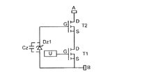
- 第1の入力端子(A)および第2の入力端子(B)と、ソースを介して前記第2の入力端子(B)へと接続され、制御ユニット(U)からもたらされる制御信号を受信するように意図されたゲート(G)を備えている第1のトランジスタ(T1)と、ゲート(G)を備えており、ドレイン(D)を介して前記第1の入力端子(A)へと接続され、ソース(S)を介して前記第1のトランジスタ(T1)へと接続された第2のトランジスタ(T2)と、を備えており、スイッチング電源システムにおいて使用されるように意図され、該スイッチング電源システムのDC/DCコンバータを制御する制御装置(1)であって、 前記第2のトランジスタ(T2)のゲート(G)および前記第2の入力端子(B)に接続され、キャパシタ(Ca)と、該キャパシタ(Ca)に直列に接続されたツェナーダイオード(Dz1)とを備えている制御アセンブリと、
前記第2のトランジスタ(T2)のゲート(G)とソース(S)との間に接続されたツェナーダイオード(Dz2)と
を備え、
1つ以上の付加型の同一パターンを備え、
各々のパターンが、
2つの接続点(M、N)と、
第1の接続点(M)へと接続されたキャパシタ(Cb)と、
前記キャパシタ(Cb)に直列に接続された第1のツェナーダイオード(Dz1)と、 前記キャパシタ(Cb)に接続されたゲート(G)と、第2の接続点(N)に接続されたソース(S)とを備える第3のトランジスタ(T3_i)と、
前記第3のトランジスタ(T3_i)のゲート(G)とソース(S)との間に接続されたツェナーダイオード(Dz3)と
を備えており、
第1の追加のパターンは、該パターンの第2の接続点(N)によって前記第2のトランジスタ(T2)のドレイン(D)へと接続されるとともに、該パターンの第1の接続点(M)によって前記第2のトランジスタ(T2)のゲート(G)へと接続され、
さらなるパターンの各々は、該パターンの第2の接続点(N)によって先行のパターンの前記トランジスタ(T3_n−1)のドレイン(D)へと接続されるとともに、該パターンの第1の接続点(M)によって先行のパターンの前記トランジスタ(T3_n−1)のゲート(G)へと接続されることを特徴とする制御装置。 - 間にDC電源が接続される第1の端子(X)および第2の端子(Y)と、前記第1の端子(X)へと接続されたDC/DCコンバータと、前記DC/DCコンバータに直列に接続され、かつ前記第2の端子(Y)に接続された制御装置(1)と、を備えるスイッチング電源システムであって、
前記制御装置(1)は、請求項1に記載の制御装置と一致することを特徴とするスイッチング電源システム。 - 前記DC/DCコンバータは絶縁「フライバック」型であることを特徴とする、請求項2に記載のシステム。
- 前記DC/DCコンバータは絶縁「フォワード」型であることを特徴とする、請求項2に記載のシステム。
- 前記DC/DCコンバータは昇圧型であることを特徴とする、請求項2に記載のシステム。
- 前記DC/DCコンバータは降圧型であることを特徴とする、請求項2に記載のシステム。
- 電気負荷(M)を制御するように意図され、
配電網(R)によってもたらされるAC電圧を整流するように意図された整流モジュール(REC)と、
前記整流モジュール(REC)へと接続され、正の電位にある第1の電源線(10)と、負の電位にある第2の電源線(11)とを備えており、前記第1および第2の電源線の間に前記整流モジュールによってもたらされる主たるDC電圧(Vbus)が加えられるDC電源バスと、
前記第1の電源線(10)と前記第2の電源線(11)とに接続されたバスキャパシタ(Cbus)と、
前記バスにおいて利用可能なDC電圧(Vbus)を前記電気負荷(M)に向けられた可変の電圧へと変換するように意図された複数のスイッチングトランジスタを備えているインバータモジュール(INV)と
を備えている可変速駆動装置であって、
請求項2から6のいずれか一項に記載のスイッチング電源システムに一致するスイッチング電源システム
を備えており、
前記スイッチング電源システムの前記第1の端子(X)は前記DC電源バスの前記第1の電源線(10)に接続され、前記スイッチング電源システムの前記第2の端子(Y)は前記DC電源バスの前記第2の電源線(11)に接続されていることを特徴とする可変速駆動装置。
Applications Claiming Priority (2)
| Application Number | Priority Date | Filing Date | Title |
|---|---|---|---|
| FR1351622 | 2013-02-25 | ||
| FR1351622A FR3002703B1 (fr) | 2013-02-25 | 2013-02-25 | Dispositif de commande employe dans un systeme d'alimentation electrique a decoupage |
Publications (3)
| Publication Number | Publication Date |
|---|---|
| JP2014166136A JP2014166136A (ja) | 2014-09-08 |
| JP2014166136A5 JP2014166136A5 (ja) | 2017-03-09 |
| JP6336294B2 true JP6336294B2 (ja) | 2018-06-06 |
Family
ID=48570273
Family Applications (1)
| Application Number | Title | Priority Date | Filing Date |
|---|---|---|---|
| JP2014033000A Active JP6336294B2 (ja) | 2013-02-25 | 2014-02-24 | スイッチング電源システムに使用される制御装置 |
Country Status (7)
| Country | Link |
|---|---|
| US (1) | US9685857B2 (ja) |
| EP (1) | EP2770636B1 (ja) |
| JP (1) | JP6336294B2 (ja) |
| CN (1) | CN104009642B (ja) |
| BR (1) | BR102014003402B1 (ja) |
| ES (1) | ES2752060T3 (ja) |
| FR (1) | FR3002703B1 (ja) |
Cited By (1)
| Publication number | Priority date | Publication date | Assignee | Title |
|---|---|---|---|---|
| JP7497938B2 (ja) | 2019-08-08 | 2024-06-11 | 日本信号株式会社 | 表示装置 |
Families Citing this family (11)
| Publication number | Priority date | Publication date | Assignee | Title |
|---|---|---|---|---|
| DE102013010188A1 (de) * | 2012-06-21 | 2013-12-24 | Fairchild Semiconductor Corp. | Schalt-Schaltkreis und Steuer- bzw. Regelschaltkreis |
| US9559608B2 (en) | 2015-03-16 | 2017-01-31 | Delphi Technologies, Inc. | Rectifier circuit with reduced reverse recovery time |
| US9762119B2 (en) * | 2015-03-27 | 2017-09-12 | Samsung Electronics Co., Ltd. | Switch driving circuit, and power factor correction circuit having the same |
| JP6639103B2 (ja) | 2015-04-15 | 2020-02-05 | 株式会社東芝 | スイッチングユニット及び電源回路 |
| JP2018042188A (ja) * | 2016-09-09 | 2018-03-15 | 株式会社東芝 | スイッチングユニットおよび電源回路 |
| WO2020012583A1 (ja) * | 2018-07-11 | 2020-01-16 | 株式会社日立産機システム | スイッチング電源回路およびそれを備えた電力変換装置 |
| CN109474269B (zh) * | 2018-10-31 | 2023-01-13 | 矽力杰半导体技术(杭州)有限公司 | 浮动开关及其驱动电路 |
| FR3097682B1 (fr) * | 2019-06-19 | 2023-01-13 | St Microelectronics Gmbh | Composant monolithique comportant un transistor de puissance au nitrure de gallium |
| US11063589B1 (en) * | 2020-04-27 | 2021-07-13 | GaN Force Corporation | Power circuit facilitating the operation of a high electron mobility transistor |
| US11764710B2 (en) | 2021-06-30 | 2023-09-19 | Texas Instruments Incorporated | Automatic transition of motor controller from open-loop control to closed-loop control |
| CN113422595B (zh) * | 2021-08-24 | 2021-11-19 | 成都市易冲半导体有限公司 | 一种处理负压ac信号的电子开关及其控制方法 |
Family Cites Families (9)
| Publication number | Priority date | Publication date | Assignee | Title |
|---|---|---|---|---|
| DE3485409D1 (de) * | 1983-10-28 | 1992-02-13 | Hitachi Ltd | Halbleiterschaltvorrichtung. |
| FR2659810B1 (fr) * | 1990-03-16 | 1992-06-05 | Merlin Gerin | Interrupteur statique moyenne tension. |
| FR2906944B1 (fr) * | 2006-10-06 | 2009-05-15 | Schneider Toshiba Inverter | Dispositif de filtrage de mode commun et variateur de vitesse comportant un tel dispositif |
| EP2001130B1 (en) * | 2007-06-05 | 2012-01-25 | Saab Ab | Gate driver circuit for a monolithic microwave integrated circuit power converter |
| JP4953034B2 (ja) * | 2010-03-26 | 2012-06-13 | Tdk株式会社 | 電圧変換器 |
| US8400789B2 (en) * | 2010-04-27 | 2013-03-19 | Power Integrations, Inc. | Power supply with input filter-controlled switch clamp circuit |
| FR2965684B1 (fr) * | 2010-10-04 | 2012-09-07 | Schneider Toshiba Inverter | Procede et systeme de commande pour reduire le courant de mode commun dans un convertisseur de puissance |
| FR2988931B1 (fr) | 2012-03-30 | 2015-10-16 | Schneider Toshiba Inverter | Dispositif de commande employe dans un systeme d'alimentation electrique a decoupage |
| TW201508908A (zh) * | 2013-08-19 | 2015-03-01 | Chunghwa Picture Tubes Ltd | 有機發光二極體的畫素電路 |
-
2013
- 2013-02-25 FR FR1351622A patent/FR3002703B1/fr not_active Expired - Fee Related
-
2014
- 2014-01-23 ES ES14152237T patent/ES2752060T3/es active Active
- 2014-01-23 EP EP14152237.5A patent/EP2770636B1/fr active Active
- 2014-02-10 US US14/176,467 patent/US9685857B2/en active Active
- 2014-02-13 BR BR102014003402-1A patent/BR102014003402B1/pt active IP Right Grant
- 2014-02-24 JP JP2014033000A patent/JP6336294B2/ja active Active
- 2014-02-25 CN CN201410063195.4A patent/CN104009642B/zh active Active
Cited By (1)
| Publication number | Priority date | Publication date | Assignee | Title |
|---|---|---|---|---|
| JP7497938B2 (ja) | 2019-08-08 | 2024-06-11 | 日本信号株式会社 | 表示装置 |
Also Published As
| Publication number | Publication date |
|---|---|
| BR102014003402B1 (pt) | 2021-02-02 |
| EP2770636A1 (fr) | 2014-08-27 |
| CN104009642A (zh) | 2014-08-27 |
| ES2752060T3 (es) | 2020-04-02 |
| FR3002703B1 (fr) | 2017-07-21 |
| JP2014166136A (ja) | 2014-09-08 |
| US9685857B2 (en) | 2017-06-20 |
| FR3002703A1 (fr) | 2014-08-29 |
| BR102014003402A2 (pt) | 2015-10-20 |
| EP2770636B1 (fr) | 2019-08-21 |
| CN104009642B (zh) | 2017-05-17 |
| US20140241015A1 (en) | 2014-08-28 |
Similar Documents
| Publication | Publication Date | Title |
|---|---|---|
| JP6336294B2 (ja) | スイッチング電源システムに使用される制御装置 | |
| JP6275391B2 (ja) | スイッチ式電力供給システムに使用される制御デバイス | |
| CN102570782B (zh) | 用于自举开关驱动器的系统和方法 | |
| US9564806B2 (en) | Boost converter with reduced switching loss and methods of operating the same | |
| KR101367607B1 (ko) | 동기형 dc-dc 컨버터 | |
| US11949328B2 (en) | Bootstrap pre-charge circuit in totem-pole power factor correction converter | |
| US20050212497A1 (en) | DC-DC converter and control method thereof | |
| US20160285386A1 (en) | Rectifier | |
| EP1872453A2 (en) | Method and apparatus for providing uninterruptible power | |
| US10020731B2 (en) | Power switch circuit | |
| CN102480216B (zh) | 用于驱动共源共栅开关的系统和方法 | |
| CN102480217A (zh) | 用于驱动开关的系统和方法 | |
| JP6794250B2 (ja) | 位相補償回路及びこれを用いたdc/dcコンバータ | |
| WO2015111154A1 (ja) | スイッチング回路、インバータ回路、及びモータ制御装置 | |
| JP5968702B2 (ja) | ノーマリーオン電界効果トランジスタを使用したインバータ・モジュールを備える電力変換器 | |
| JPWO2015072098A1 (ja) | ゲート駆動回路およびそれを用いた電力変換装置 | |
| US10056837B2 (en) | DC-DC converter and power source device | |
| CN106849648A (zh) | 同步调节中的电流阈值检测 | |
| US9866104B2 (en) | Circuits and methods for operating a switching regulator | |
| JP6794249B2 (ja) | 位相補償回路及びこれを用いたdc/dcコンバータ | |
| CN106160480A (zh) | 功率变换器装置 | |
| JP2002354799A (ja) | スイッチング電源装置 | |
| US12160230B2 (en) | Switching circuit apparatus capable of controlling multiple switching elements to synchronously turn on and off with bootstrap circuit | |
| Hannon et al. | Design and optimisation of a high current, high frequency monolithic buck converter | |
| KR20190135252A (ko) | 부스트 컨버터 |
Legal Events
| Date | Code | Title | Description |
|---|---|---|---|
| A621 | Written request for application examination |
Free format text: JAPANESE INTERMEDIATE CODE: A621 Effective date: 20160831 |
|
| RD03 | Notification of appointment of power of attorney |
Free format text: JAPANESE INTERMEDIATE CODE: A7423 Effective date: 20161212 |
|
| A521 | Request for written amendment filed |
Free format text: JAPANESE INTERMEDIATE CODE: A523 Effective date: 20170201 |
|
| A131 | Notification of reasons for refusal |
Free format text: JAPANESE INTERMEDIATE CODE: A131 Effective date: 20170804 |
|
| A521 | Request for written amendment filed |
Free format text: JAPANESE INTERMEDIATE CODE: A523 Effective date: 20171101 |
|
| A02 | Decision of refusal |
Free format text: JAPANESE INTERMEDIATE CODE: A02 Effective date: 20171114 |
|
| A521 | Request for written amendment filed |
Free format text: JAPANESE INTERMEDIATE CODE: A523 Effective date: 20180313 |
|
| A911 | Transfer to examiner for re-examination before appeal (zenchi) |
Free format text: JAPANESE INTERMEDIATE CODE: A911 Effective date: 20180319 |
|
| TRDD | Decision of grant or rejection written | ||
| A01 | Written decision to grant a patent or to grant a registration (utility model) |
Free format text: JAPANESE INTERMEDIATE CODE: A01 Effective date: 20180406 |
|
| A61 | First payment of annual fees (during grant procedure) |
Free format text: JAPANESE INTERMEDIATE CODE: A61 Effective date: 20180502 |
|
| R150 | Certificate of patent or registration of utility model |
Ref document number: 6336294 Country of ref document: JP Free format text: JAPANESE INTERMEDIATE CODE: R150 |
|
| R250 | Receipt of annual fees |
Free format text: JAPANESE INTERMEDIATE CODE: R250 |
|
| R250 | Receipt of annual fees |
Free format text: JAPANESE INTERMEDIATE CODE: R250 |
|
| R250 | Receipt of annual fees |
Free format text: JAPANESE INTERMEDIATE CODE: R250 |
|
| R250 | Receipt of annual fees |
Free format text: JAPANESE INTERMEDIATE CODE: R250 |