JP6301034B1 - 有機elデバイスの製造方法 - Google Patents
有機elデバイスの製造方法 Download PDFInfo
- Publication number
- JP6301034B1 JP6301034B1 JP2017559137A JP2017559137A JP6301034B1 JP 6301034 B1 JP6301034 B1 JP 6301034B1 JP 2017559137 A JP2017559137 A JP 2017559137A JP 2017559137 A JP2017559137 A JP 2017559137A JP 6301034 B1 JP6301034 B1 JP 6301034B1
- Authority
- JP
- Japan
- Prior art keywords
- layer
- organic
- barrier layer
- inorganic
- inorganic barrier
- Prior art date
- Legal status (The legal status is an assumption and is not a legal conclusion. Google has not performed a legal analysis and makes no representation as to the accuracy of the status listed.)
- Expired - Fee Related
Links
Images





Classifications
-
- H—ELECTRICITY
- H10—SEMICONDUCTOR DEVICES; ELECTRIC SOLID-STATE DEVICES NOT OTHERWISE PROVIDED FOR
- H10D—INORGANIC ELECTRIC SEMICONDUCTOR DEVICES
- H10D86/00—Integrated devices formed in or on insulating or conducting substrates, e.g. formed in silicon-on-insulator [SOI] substrates or on stainless steel or glass substrates
- H10D86/40—Integrated devices formed in or on insulating or conducting substrates, e.g. formed in silicon-on-insulator [SOI] substrates or on stainless steel or glass substrates characterised by multiple TFTs
- H10D86/411—Integrated devices formed in or on insulating or conducting substrates, e.g. formed in silicon-on-insulator [SOI] substrates or on stainless steel or glass substrates characterised by multiple TFTs characterised by materials, geometry or structure of the substrates
-
- H—ELECTRICITY
- H10—SEMICONDUCTOR DEVICES; ELECTRIC SOLID-STATE DEVICES NOT OTHERWISE PROVIDED FOR
- H10D—INORGANIC ELECTRIC SEMICONDUCTOR DEVICES
- H10D86/00—Integrated devices formed in or on insulating or conducting substrates, e.g. formed in silicon-on-insulator [SOI] substrates or on stainless steel or glass substrates
- H10D86/40—Integrated devices formed in or on insulating or conducting substrates, e.g. formed in silicon-on-insulator [SOI] substrates or on stainless steel or glass substrates characterised by multiple TFTs
- H10D86/421—Integrated devices formed in or on insulating or conducting substrates, e.g. formed in silicon-on-insulator [SOI] substrates or on stainless steel or glass substrates characterised by multiple TFTs having a particular composition, shape or crystalline structure of the active layer
- H10D86/423—Integrated devices formed in or on insulating or conducting substrates, e.g. formed in silicon-on-insulator [SOI] substrates or on stainless steel or glass substrates characterised by multiple TFTs having a particular composition, shape or crystalline structure of the active layer comprising semiconductor materials not belonging to the Group IV, e.g. InGaZnO
-
- H—ELECTRICITY
- H10—SEMICONDUCTOR DEVICES; ELECTRIC SOLID-STATE DEVICES NOT OTHERWISE PROVIDED FOR
- H10D—INORGANIC ELECTRIC SEMICONDUCTOR DEVICES
- H10D86/00—Integrated devices formed in or on insulating or conducting substrates, e.g. formed in silicon-on-insulator [SOI] substrates or on stainless steel or glass substrates
- H10D86/40—Integrated devices formed in or on insulating or conducting substrates, e.g. formed in silicon-on-insulator [SOI] substrates or on stainless steel or glass substrates characterised by multiple TFTs
- H10D86/441—Interconnections, e.g. scanning lines
-
- H—ELECTRICITY
- H10—SEMICONDUCTOR DEVICES; ELECTRIC SOLID-STATE DEVICES NOT OTHERWISE PROVIDED FOR
- H10D—INORGANIC ELECTRIC SEMICONDUCTOR DEVICES
- H10D86/00—Integrated devices formed in or on insulating or conducting substrates, e.g. formed in silicon-on-insulator [SOI] substrates or on stainless steel or glass substrates
- H10D86/40—Integrated devices formed in or on insulating or conducting substrates, e.g. formed in silicon-on-insulator [SOI] substrates or on stainless steel or glass substrates characterised by multiple TFTs
- H10D86/451—Integrated devices formed in or on insulating or conducting substrates, e.g. formed in silicon-on-insulator [SOI] substrates or on stainless steel or glass substrates characterised by multiple TFTs characterised by the compositions or shapes of the interlayer dielectrics
-
- H—ELECTRICITY
- H10—SEMICONDUCTOR DEVICES; ELECTRIC SOLID-STATE DEVICES NOT OTHERWISE PROVIDED FOR
- H10D—INORGANIC ELECTRIC SEMICONDUCTOR DEVICES
- H10D86/00—Integrated devices formed in or on insulating or conducting substrates, e.g. formed in silicon-on-insulator [SOI] substrates or on stainless steel or glass substrates
- H10D86/40—Integrated devices formed in or on insulating or conducting substrates, e.g. formed in silicon-on-insulator [SOI] substrates or on stainless steel or glass substrates characterised by multiple TFTs
- H10D86/60—Integrated devices formed in or on insulating or conducting substrates, e.g. formed in silicon-on-insulator [SOI] substrates or on stainless steel or glass substrates characterised by multiple TFTs wherein the TFTs are in active matrices
-
- H—ELECTRICITY
- H10—SEMICONDUCTOR DEVICES; ELECTRIC SOLID-STATE DEVICES NOT OTHERWISE PROVIDED FOR
- H10K—ORGANIC ELECTRIC SOLID-STATE DEVICES
- H10K50/00—Organic light-emitting devices
- H10K50/80—Constructional details
- H10K50/84—Passivation; Containers; Encapsulations
- H10K50/844—Encapsulations
-
- H—ELECTRICITY
- H10—SEMICONDUCTOR DEVICES; ELECTRIC SOLID-STATE DEVICES NOT OTHERWISE PROVIDED FOR
- H10K—ORGANIC ELECTRIC SOLID-STATE DEVICES
- H10K59/00—Integrated devices, or assemblies of multiple devices, comprising at least one organic light-emitting element covered by group H10K50/00
- H10K59/10—OLED displays
- H10K59/12—Active-matrix OLED [AMOLED] displays
- H10K59/1201—Manufacture or treatment
-
- H—ELECTRICITY
- H10—SEMICONDUCTOR DEVICES; ELECTRIC SOLID-STATE DEVICES NOT OTHERWISE PROVIDED FOR
- H10K—ORGANIC ELECTRIC SOLID-STATE DEVICES
- H10K59/00—Integrated devices, or assemblies of multiple devices, comprising at least one organic light-emitting element covered by group H10K50/00
- H10K59/10—OLED displays
- H10K59/12—Active-matrix OLED [AMOLED] displays
- H10K59/124—Insulating layers formed between TFT elements and OLED elements
-
- H—ELECTRICITY
- H10—SEMICONDUCTOR DEVICES; ELECTRIC SOLID-STATE DEVICES NOT OTHERWISE PROVIDED FOR
- H10K—ORGANIC ELECTRIC SOLID-STATE DEVICES
- H10K59/00—Integrated devices, or assemblies of multiple devices, comprising at least one organic light-emitting element covered by group H10K50/00
- H10K59/10—OLED displays
- H10K59/12—Active-matrix OLED [AMOLED] displays
- H10K59/131—Interconnections, e.g. wiring lines or terminals
-
- H—ELECTRICITY
- H10—SEMICONDUCTOR DEVICES; ELECTRIC SOLID-STATE DEVICES NOT OTHERWISE PROVIDED FOR
- H10K—ORGANIC ELECTRIC SOLID-STATE DEVICES
- H10K59/00—Integrated devices, or assemblies of multiple devices, comprising at least one organic light-emitting element covered by group H10K50/00
- H10K59/80—Constructional details
- H10K59/87—Passivation; Containers; Encapsulations
- H10K59/873—Encapsulations
-
- H—ELECTRICITY
- H10—SEMICONDUCTOR DEVICES; ELECTRIC SOLID-STATE DEVICES NOT OTHERWISE PROVIDED FOR
- H10K—ORGANIC ELECTRIC SOLID-STATE DEVICES
- H10K71/00—Manufacture or treatment specially adapted for the organic devices covered by this subclass
-
- H—ELECTRICITY
- H10—SEMICONDUCTOR DEVICES; ELECTRIC SOLID-STATE DEVICES NOT OTHERWISE PROVIDED FOR
- H10K—ORGANIC ELECTRIC SOLID-STATE DEVICES
- H10K71/00—Manufacture or treatment specially adapted for the organic devices covered by this subclass
- H10K71/40—Thermal treatment, e.g. annealing in the presence of a solvent vapour
-
- H—ELECTRICITY
- H10—SEMICONDUCTOR DEVICES; ELECTRIC SOLID-STATE DEVICES NOT OTHERWISE PROVIDED FOR
- H10K—ORGANIC ELECTRIC SOLID-STATE DEVICES
- H10K77/00—Constructional details of devices covered by this subclass and not covered by groups H10K10/80, H10K30/80, H10K50/80 or H10K59/80
- H10K77/10—Substrates, e.g. flexible substrates
- H10K77/111—Flexible substrates
-
- H—ELECTRICITY
- H10—SEMICONDUCTOR DEVICES; ELECTRIC SOLID-STATE DEVICES NOT OTHERWISE PROVIDED FOR
- H10K—ORGANIC ELECTRIC SOLID-STATE DEVICES
- H10K2102/00—Constructional details relating to the organic devices covered by this subclass
- H10K2102/301—Details of OLEDs
- H10K2102/311—Flexible OLED
-
- Y—GENERAL TAGGING OF NEW TECHNOLOGICAL DEVELOPMENTS; GENERAL TAGGING OF CROSS-SECTIONAL TECHNOLOGIES SPANNING OVER SEVERAL SECTIONS OF THE IPC; TECHNICAL SUBJECTS COVERED BY FORMER USPC CROSS-REFERENCE ART COLLECTIONS [XRACs] AND DIGESTS
- Y02—TECHNOLOGIES OR APPLICATIONS FOR MITIGATION OR ADAPTATION AGAINST CLIMATE CHANGE
- Y02E—REDUCTION OF GREENHOUSE GAS [GHG] EMISSIONS, RELATED TO ENERGY GENERATION, TRANSMISSION OR DISTRIBUTION
- Y02E10/00—Energy generation through renewable energy sources
- Y02E10/50—Photovoltaic [PV] energy
- Y02E10/549—Organic PV cells
-
- Y—GENERAL TAGGING OF NEW TECHNOLOGICAL DEVELOPMENTS; GENERAL TAGGING OF CROSS-SECTIONAL TECHNOLOGIES SPANNING OVER SEVERAL SECTIONS OF THE IPC; TECHNICAL SUBJECTS COVERED BY FORMER USPC CROSS-REFERENCE ART COLLECTIONS [XRACs] AND DIGESTS
- Y02—TECHNOLOGIES OR APPLICATIONS FOR MITIGATION OR ADAPTATION AGAINST CLIMATE CHANGE
- Y02P—CLIMATE CHANGE MITIGATION TECHNOLOGIES IN THE PRODUCTION OR PROCESSING OF GOODS
- Y02P70/00—Climate change mitigation technologies in the production process for final industrial or consumer products
- Y02P70/50—Manufacturing or production processes characterised by the final manufactured product
Landscapes
- Engineering & Computer Science (AREA)
- Microelectronics & Electronic Packaging (AREA)
- Manufacturing & Machinery (AREA)
- Physics & Mathematics (AREA)
- Optics & Photonics (AREA)
- Electroluminescent Light Sources (AREA)
- Devices For Indicating Variable Information By Combining Individual Elements (AREA)
Abstract
Description
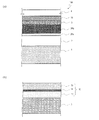
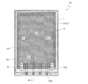
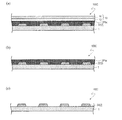
2 :バックプレーン(回路)
3 :有機EL素子
4 :偏光板
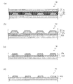
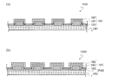
10 :薄膜封止構造(TFE構造)
12 :第1無機バリア層(SiNx層)
14 :有機バリア層(アクリル樹脂層)
16 :第2無機バリア層(SiNx層)
20 :素子基板
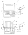
26 :アクリルモノマー
26p :アクリルモノマーの蒸気または霧状のアクリルモノマー
100、100C :有機EL表示装置
200 :成膜装置
Claims (12)
- 有機ELデバイスの製造方法であって、
前記有機ELデバイスは、基板と、前記基板上に形成された複数のTFTと、それぞれが前記複数のTFTのいずれかに接続された複数のゲートバスラインおよび複数のソースバスラインと、複数の端子と、前記複数の端子と前記複数のゲートバスラインまたは前記複数のソースバスラインのいずれかとを接続する複数の引出し配線とを有する、駆動回路層と、前記駆動回路層上に形成され、少なくとも前記複数の端子を露出する無機保護層と、前記無機保護層上に形成された有機平坦化層と、前記有機平坦化層上に形成され、それぞれが前記複数のTFTのいずれかに接続された複数の有機EL素子を有する有機EL素子層と、前記有機EL素子層を覆うように形成された薄膜封止構造とを有し、
前記製造方法は、
前記基板上に前記駆動回路層を形成する工程Aと、
前記駆動回路層上に前記無機保護層を形成する工程Bと、
前記無機保護層上に前記有機平坦化層を形成する工程Cと、
前記有機平坦化層を200℃以上の温度に加熱する工程Dと、
前記加熱工程の後に、前記有機平坦化層上に、前記有機EL素子層を形成する工程Eと
を包含し、
前記工程Cの後、かつ前記工程Dの前に、前記有機平坦化層を覆う有機高分子膜を形成する工程C1と、前記有機高分子膜を除去する工程C2とをさらに包含する、製造方法。 - 前記工程C1と前記工程C2との間に、前記有機高分子膜が形成された前記基板を保管または運搬する工程をさらに包含する、請求項1に記載の製造方法。
- 前記工程C1は、前記有機高分子の溶液を前記有機平坦化層上に付与する工程を包含する、請求項1また2に記載の製造方法。
- 前記有機高分子膜は、水溶性高分子から形成されている、請求項1から3のいずれかに記載の製造方法。
- 前記工程C2は、水系溶媒で前記有機高分子膜を溶解させる工程を包含する、請求項4に記載の製造方法。
- 前記水溶性高分子は、ポリビニルアルコールである、請求項4または5に記載の製造方法。
- 前記有機平坦化層は、感光性を有する樹脂から形成されている、請求項1から6のいずれかに記載の製造方法。
- 前記有機平坦化層は、ポリイミドから形成されている、請求項1から7のいずれかに記載の製造方法。
- 前記基板の法線方向から見たとき、前記無機保護層が形成された領域内に、前記有機平坦化層が形成されており、前記有機平坦化層が形成された領域内に、前記複数の有機EL素子が配置されており、前記薄膜封止構造の外縁は、前記複数の引出し配線と交差し、かつ、前記有機平坦化層の外縁と前記無機保護層の外縁との間に存在し、
前記薄膜封止構造は、前記有機EL層上に形成された第1無機バリア層と、前記第1無機バリア層の上に形成された有機バリア層と、前記有機バリア層の上に形成された第2無機バリア層とを有し、
前記複数の引出し配線の上で前記無機保護層と前記第1無機バリア層とが直接接触する部分において、前記第1無機バリア層の、前記複数の引出し配線の線幅方向に平行な断面の形状における側面のテーパー角は、90°未満である、請求項1から8のいずれかに記載の製造方法。
- 前記第1無機バリア層の前記側面の前記テーパー角は70°未満である、請求項9に記載の製造方法。
- 前記工程Eの後で、前記複数の有機EL素子が形成されたアクティブ領域に選択的に前記第1無機バリア層を形成する工程Fと、
前記工程Fの後で、前記基板をチャンバー内に配置し、前記チャンバー内に蒸気または霧状の光硬化性樹脂を供給する工程Gと、
前記第1無機バリア層上で光硬化性樹脂を凝縮させる工程であって、前記テーパー角が90°未満の前記第1無機バリア層の部分の上には、前記光硬化性樹脂を存在させないように、前記光硬化性樹脂を凝縮させる工程Hと、
前記工程Hの後に、前記凝縮された前記光硬化性樹脂に光を照射することによって、光硬化樹脂からなる前記有機バリア層を形成する工程Iと
を包含する、請求項9または10に記載の製造方法。 - 前記工程Eの後で、前記複数の有機EL素子が形成されたアクティブ領域に選択的に前記第1無機バリア層を形成する工程Fと、
前記工程Fの後で、前記基板をチャンバー内に配置し、前記チャンバー内に蒸気または霧状の光硬化性樹脂を供給する工程Gと、
前記第1無機バリア層上で前記光硬化性樹脂を凝縮させ、液状の膜を形成する工程Hと、
前記光硬化性樹脂の前記液状の膜に光を照射することによって、光硬化樹脂層を形成する工程Iと、
前記光硬化樹脂層を部分的にアッシングすることによって、前記有機バリア層を形成する工程Jと
を包含する、請求項9または10に記載の製造方法。
Applications Claiming Priority (1)
| Application Number | Priority Date | Filing Date | Title |
|---|---|---|---|
| PCT/JP2017/023589 WO2019003305A1 (ja) | 2017-06-27 | 2017-06-27 | 有機elデバイスの製造方法 |
Related Child Applications (1)
| Application Number | Title | Priority Date | Filing Date |
|---|---|---|---|
| JP2018033144A Division JP6542931B2 (ja) | 2018-02-27 | 2018-02-27 | 有機elデバイスの製造方法 |
Publications (2)
| Publication Number | Publication Date |
|---|---|
| JP6301034B1 true JP6301034B1 (ja) | 2018-03-28 |
| JPWO2019003305A1 JPWO2019003305A1 (ja) | 2019-06-27 |
Family
ID=61756588
Family Applications (1)
| Application Number | Title | Priority Date | Filing Date |
|---|---|---|---|
| JP2017559137A Expired - Fee Related JP6301034B1 (ja) | 2017-06-27 | 2017-06-27 | 有機elデバイスの製造方法 |
Country Status (4)
| Country | Link |
|---|---|
| US (2) | US10276837B2 (ja) |
| JP (1) | JP6301034B1 (ja) |
| CN (2) | CN111799316A (ja) |
| WO (1) | WO2019003305A1 (ja) |
Cited By (7)
| Publication number | Priority date | Publication date | Assignee | Title |
|---|---|---|---|---|
| WO2019186825A1 (ja) * | 2018-03-28 | 2019-10-03 | 堺ディスプレイプロダクト株式会社 | 有機el表示装置およびその製造方法 |
| WO2019186824A1 (ja) * | 2018-03-28 | 2019-10-03 | 堺ディスプレイプロダクト株式会社 | 有機el表示装置およびその製造方法 |
| WO2019202739A1 (ja) * | 2018-04-20 | 2019-10-24 | 堺ディスプレイプロダクト株式会社 | 有機elデバイスおよびその製造方法 |
| WO2019202738A1 (ja) * | 2018-04-20 | 2019-10-24 | 堺ディスプレイプロダクト株式会社 | 有機elデバイスおよびその製造方法 |
| JP2020074312A (ja) * | 2018-04-20 | 2020-05-14 | 堺ディスプレイプロダクト株式会社 | 有機elデバイスおよびその製造方法 |
| JP2020102456A (ja) * | 2020-02-18 | 2020-07-02 | 堺ディスプレイプロダクト株式会社 | 有機elデバイスおよびその製造方法 |
| US11107876B2 (en) | 2018-04-26 | 2021-08-31 | Sakai Display Products Corporation | Organic electroluminescent device and method for producing same |
Families Citing this family (10)
| Publication number | Priority date | Publication date | Assignee | Title |
|---|---|---|---|---|
| JP6054763B2 (ja) | 2013-02-12 | 2016-12-27 | 株式会社ジャパンディスプレイ | 有機el表示装置 |
| US10734599B2 (en) * | 2016-06-30 | 2020-08-04 | Hon Hai Precision Industry Co., Ltd. | Organic EL display device and method for manufacturing same |
| CN114899346B (zh) | 2017-06-13 | 2025-07-29 | 堺显示器制品株式会社 | 有机el设备的制造方法及薄膜密封结构形成装置 |
| US10754387B2 (en) * | 2017-09-29 | 2020-08-25 | Sharp Kabushiki Kaisha | Flexible display device |
| US10581028B2 (en) * | 2017-11-29 | 2020-03-03 | Sakai Display Products Corporation | Method for producing organic electroluminescent display device |
| CN109920330B (zh) * | 2019-02-22 | 2021-03-05 | 合肥鑫晟光电科技有限公司 | 一种基板和显示装置 |
| US11341925B2 (en) | 2019-05-02 | 2022-05-24 | Dell Products L.P. | Information handling system adapting multiple display visual image presentations |
| US11017742B2 (en) * | 2019-05-02 | 2021-05-25 | Dell Products L.P. | Information handling system multiple display viewing angle brightness adjustment |
| CN110875369A (zh) * | 2019-11-27 | 2020-03-10 | 京东方科技集团股份有限公司 | 显示背板、显示面板及其制作方法和显示装置 |
| KR20250007680A (ko) * | 2020-05-29 | 2025-01-14 | 보에 테크놀로지 그룹 컴퍼니 리미티드 | 표시패널 및 이의 제조방법, 표시장치 |
Citations (3)
| Publication number | Priority date | Publication date | Assignee | Title |
|---|---|---|---|---|
| JP2009117079A (ja) * | 2007-11-02 | 2009-05-28 | Seiko Epson Corp | 有機エレクトロルミネッセンス装置およびその製造方法、電子機器 |
| JP2015079618A (ja) * | 2013-10-16 | 2015-04-23 | 凸版印刷株式会社 | 薄膜トランジスタ基板及びその製造方法、薄膜トランジスタ基板を用いた有機el素子及びその製造方法 |
| JP2016003384A (ja) * | 2014-06-19 | 2016-01-12 | 株式会社Joled | マスク及び有機発光デバイスの製造方法 |
Family Cites Families (13)
| Publication number | Priority date | Publication date | Assignee | Title |
|---|---|---|---|---|
| JP4185341B2 (ja) * | 2002-09-25 | 2008-11-26 | パイオニア株式会社 | 多層バリア膜構造、有機エレクトロルミネッセンス表示パネル及び製造方法 |
| JP2004119317A (ja) * | 2002-09-27 | 2004-04-15 | Toshiba Corp | 有機エレクトロルミネッセンス表示装置 |
| JP4792717B2 (ja) * | 2004-07-07 | 2011-10-12 | セイコーエプソン株式会社 | 電気光学装置、電気光学装置の製造方法、及び電子機器 |
| JP4950673B2 (ja) * | 2007-01-10 | 2012-06-13 | キヤノン株式会社 | 有機el表示装置 |
| WO2011132353A1 (ja) * | 2010-04-19 | 2011-10-27 | シャープ株式会社 | 表示装置及びその製造方法 |
| JP4975137B2 (ja) * | 2010-04-19 | 2012-07-11 | キヤノン株式会社 | 有機el素子および表示装置 |
| KR101756656B1 (ko) * | 2010-06-25 | 2017-07-11 | 엘지디스플레이 주식회사 | 터치 패널 내장형 유기발광다이오드 표시 장치 |
| JP5981115B2 (ja) | 2011-09-20 | 2016-08-31 | 株式会社アルバック | 成膜装置 |
| JP5988619B2 (ja) | 2012-03-06 | 2016-09-07 | 株式会社アルバック | 成膜装置、成膜方法 |
| CN105284186B (zh) * | 2013-06-07 | 2017-05-17 | 株式会社爱发科 | 元件结构体及其制造方法 |
| JP2015149467A (ja) * | 2014-01-10 | 2015-08-20 | 株式会社Joled | 薄膜トランジスタ基板の製造方法 |
| JP6307384B2 (ja) | 2014-08-11 | 2018-04-04 | 株式会社ジャパンディスプレイ | 有機el表示装置 |
| CN105590848B (zh) * | 2014-11-17 | 2019-02-15 | 上海和辉光电有限公司 | 显示器件制备方法 |
-
2017
- 2017-06-27 CN CN202010721889.8A patent/CN111799316A/zh active Pending
- 2017-06-27 WO PCT/JP2017/023589 patent/WO2019003305A1/ja not_active Ceased
- 2017-06-27 US US15/750,593 patent/US10276837B2/en not_active Expired - Fee Related
- 2017-06-27 CN CN201780003621.7A patent/CN109429571B/zh not_active Expired - Fee Related
- 2017-06-27 JP JP2017559137A patent/JP6301034B1/ja not_active Expired - Fee Related
-
2019
- 2019-03-13 US US16/351,770 patent/US10461284B2/en not_active Expired - Fee Related
Patent Citations (3)
| Publication number | Priority date | Publication date | Assignee | Title |
|---|---|---|---|---|
| JP2009117079A (ja) * | 2007-11-02 | 2009-05-28 | Seiko Epson Corp | 有機エレクトロルミネッセンス装置およびその製造方法、電子機器 |
| JP2015079618A (ja) * | 2013-10-16 | 2015-04-23 | 凸版印刷株式会社 | 薄膜トランジスタ基板及びその製造方法、薄膜トランジスタ基板を用いた有機el素子及びその製造方法 |
| JP2016003384A (ja) * | 2014-06-19 | 2016-01-12 | 株式会社Joled | マスク及び有機発光デバイスの製造方法 |
Cited By (20)
| Publication number | Priority date | Publication date | Assignee | Title |
|---|---|---|---|---|
| JPWO2019186824A1 (ja) * | 2018-03-28 | 2020-04-30 | 堺ディスプレイプロダクト株式会社 | 有機el表示装置およびその製造方法 |
| WO2019186824A1 (ja) * | 2018-03-28 | 2019-10-03 | 堺ディスプレイプロダクト株式会社 | 有機el表示装置およびその製造方法 |
| WO2019186825A1 (ja) * | 2018-03-28 | 2019-10-03 | 堺ディスプレイプロダクト株式会社 | 有機el表示装置およびその製造方法 |
| JPWO2019186825A1 (ja) * | 2018-03-28 | 2020-04-30 | 堺ディスプレイプロダクト株式会社 | 有機el表示装置およびその製造方法 |
| CN111937490A (zh) * | 2018-04-20 | 2020-11-13 | 堺显示器制品株式会社 | 有机el装置及其制造方法 |
| JP2021114470A (ja) * | 2018-04-20 | 2021-08-05 | 堺ディスプレイプロダクト株式会社 | 有機elデバイスの製造方法 |
| WO2019202738A1 (ja) * | 2018-04-20 | 2019-10-24 | 堺ディスプレイプロダクト株式会社 | 有機elデバイスおよびその製造方法 |
| JP2020074312A (ja) * | 2018-04-20 | 2020-05-14 | 堺ディスプレイプロダクト株式会社 | 有機elデバイスおよびその製造方法 |
| JP6648349B1 (ja) * | 2018-04-20 | 2020-02-14 | 堺ディスプレイプロダクト株式会社 | 有機elデバイスおよびその製造方法 |
| JPWO2019202738A1 (ja) * | 2018-04-20 | 2020-09-24 | 堺ディスプレイプロダクト株式会社 | 有機elデバイスおよびその製造方法 |
| WO2019202739A1 (ja) * | 2018-04-20 | 2019-10-24 | 堺ディスプレイプロダクト株式会社 | 有機elデバイスおよびその製造方法 |
| US11950488B2 (en) | 2018-04-20 | 2024-04-02 | Sakai Display Products Corporation | Organic electroluminescent device and method for producing same |
| US11825683B2 (en) | 2018-04-20 | 2023-11-21 | Sakai Display Products Corporation | Organic electroluminescent device including thin film encapsulation structure and method for producing same |
| JP7076027B2 (ja) | 2018-04-20 | 2022-05-26 | 堺ディスプレイプロダクト株式会社 | 有機elデバイスの製造方法 |
| US12402492B2 (en) | 2018-04-20 | 2025-08-26 | Sakai Display Products Corporation | Organic electroluminescent device including thin film encapsulation structure and method for producing same |
| CN111937490B (zh) * | 2018-04-20 | 2023-07-18 | 堺显示器制品株式会社 | 有机el装置及其制造方法 |
| US11711955B2 (en) | 2018-04-26 | 2023-07-25 | Sakai Display Products Corporation | Organic electroluminescent device with organic flattening layer having surface Ra of 50 nm or less and method for producing same |
| US11107876B2 (en) | 2018-04-26 | 2021-08-31 | Sakai Display Products Corporation | Organic electroluminescent device and method for producing same |
| JP2020102456A (ja) * | 2020-02-18 | 2020-07-02 | 堺ディスプレイプロダクト株式会社 | 有機elデバイスおよびその製造方法 |
| JP7109492B2 (ja) | 2020-02-18 | 2022-07-29 | 堺ディスプレイプロダクト株式会社 | 有機elデバイスの製造方法 |
Also Published As
| Publication number | Publication date |
|---|---|
| US20190019993A1 (en) | 2019-01-17 |
| US20190280249A1 (en) | 2019-09-12 |
| US10276837B2 (en) | 2019-04-30 |
| JPWO2019003305A1 (ja) | 2019-06-27 |
| CN111799316A (zh) | 2020-10-20 |
| US10461284B2 (en) | 2019-10-29 |
| CN109429571B (zh) | 2020-08-18 |
| WO2019003305A1 (ja) | 2019-01-03 |
| CN109429571A (zh) | 2019-03-05 |
Similar Documents
| Publication | Publication Date | Title |
|---|---|---|
| JP6301034B1 (ja) | 有機elデバイスの製造方法 | |
| JP6321310B1 (ja) | 有機elデバイスおよびその製造方法 | |
| CN110447307B (zh) | 有机el器件及其制造方法 | |
| JP6648349B1 (ja) | 有機elデバイスおよびその製造方法 | |
| JP7076027B2 (ja) | 有機elデバイスの製造方法 | |
| JP6664567B1 (ja) | 有機elデバイスおよびその製造方法 | |
| JP6567121B2 (ja) | 薄膜封止構造形成装置 | |
| JP6542931B2 (ja) | 有機elデバイスの製造方法 | |
| JP6942208B2 (ja) | 有機elデバイスおよびその製造方法 | |
| JP6872586B2 (ja) | 有機elデバイスの製造方法 | |
| JP7109492B2 (ja) | 有機elデバイスの製造方法 |
Legal Events
| Date | Code | Title | Description |
|---|---|---|---|
| A621 | Written request for application examination |
Free format text: JAPANESE INTERMEDIATE CODE: A621 Effective date: 20171110 |
|
| A871 | Explanation of circumstances concerning accelerated examination |
Free format text: JAPANESE INTERMEDIATE CODE: A871 Effective date: 20171110 |
|
| A975 | Report on accelerated examination |
Free format text: JAPANESE INTERMEDIATE CODE: A971005 Effective date: 20171211 |
|
| A131 | Notification of reasons for refusal |
Free format text: JAPANESE INTERMEDIATE CODE: A131 Effective date: 20171219 |
|
| A521 | Request for written amendment filed |
Free format text: JAPANESE INTERMEDIATE CODE: A523 Effective date: 20180111 |
|
| TRDD | Decision of grant or rejection written | ||
| A01 | Written decision to grant a patent or to grant a registration (utility model) |
Free format text: JAPANESE INTERMEDIATE CODE: A01 Effective date: 20180206 |
|
| A61 | First payment of annual fees (during grant procedure) |
Free format text: JAPANESE INTERMEDIATE CODE: A61 Effective date: 20180227 |
|
| R150 | Certificate of patent or registration of utility model |
Ref document number: 6301034 Country of ref document: JP Free format text: JAPANESE INTERMEDIATE CODE: R150 |
|
| R250 | Receipt of annual fees |
Free format text: JAPANESE INTERMEDIATE CODE: R250 |
|
| LAPS | Cancellation because of no payment of annual fees |