JP6285158B2 - 有機el表示装置 - Google Patents
有機el表示装置 Download PDFInfo
- Publication number
- JP6285158B2 JP6285158B2 JP2013243783A JP2013243783A JP6285158B2 JP 6285158 B2 JP6285158 B2 JP 6285158B2 JP 2013243783 A JP2013243783 A JP 2013243783A JP 2013243783 A JP2013243783 A JP 2013243783A JP 6285158 B2 JP6285158 B2 JP 6285158B2
- Authority
- JP
- Japan
- Prior art keywords
- light emitting
- emitting element
- current
- pixel
- gradation
- Prior art date
- Legal status (The legal status is an assumption and is not a legal conclusion. Google has not performed a legal analysis and makes no representation as to the accuracy of the status listed.)
- Active
Links
- 230000004044 response Effects 0.000 claims 2
- 238000005401 electroluminescence Methods 0.000 description 30
- 238000010586 diagram Methods 0.000 description 17
- 239000000758 substrate Substances 0.000 description 15
- 230000007423 decrease Effects 0.000 description 12
- 239000010409 thin film Substances 0.000 description 6
- 239000011521 glass Substances 0.000 description 5
- 239000011159 matrix material Substances 0.000 description 5
- 102100036464 Activated RNA polymerase II transcriptional coactivator p15 Human genes 0.000 description 3
- 101000713904 Homo sapiens Activated RNA polymerase II transcriptional coactivator p15 Proteins 0.000 description 3
- 229910004444 SUB1 Inorganic materials 0.000 description 3
- 239000003990 capacitor Substances 0.000 description 3
- 229910004438 SUB2 Inorganic materials 0.000 description 2
- 101100311330 Schizosaccharomyces pombe (strain 972 / ATCC 24843) uap56 gene Proteins 0.000 description 2
- 239000003086 colorant Substances 0.000 description 2
- 238000000295 emission spectrum Methods 0.000 description 2
- 239000010408 film Substances 0.000 description 2
- 238000000034 method Methods 0.000 description 2
- 101150018444 sub2 gene Proteins 0.000 description 2
- 239000000470 constituent Substances 0.000 description 1
- 230000003247 decreasing effect Effects 0.000 description 1
- 230000000694 effects Effects 0.000 description 1
- 230000005611 electricity Effects 0.000 description 1
- 230000006870 function Effects 0.000 description 1
- 238000004519 manufacturing process Methods 0.000 description 1
Images


Classifications
-
- G—PHYSICS
- G09—EDUCATION; CRYPTOGRAPHY; DISPLAY; ADVERTISING; SEALS
- G09G—ARRANGEMENTS OR CIRCUITS FOR CONTROL OF INDICATING DEVICES USING STATIC MEANS TO PRESENT VARIABLE INFORMATION
- G09G3/00—Control arrangements or circuits, of interest only in connection with visual indicators other than cathode-ray tubes
- G09G3/20—Control arrangements or circuits, of interest only in connection with visual indicators other than cathode-ray tubes for presentation of an assembly of a number of characters, e.g. a page, by composing the assembly by combination of individual elements arranged in a matrix no fixed position being assigned to or needed to be assigned to the individual characters or partial characters
- G09G3/22—Control arrangements or circuits, of interest only in connection with visual indicators other than cathode-ray tubes for presentation of an assembly of a number of characters, e.g. a page, by composing the assembly by combination of individual elements arranged in a matrix no fixed position being assigned to or needed to be assigned to the individual characters or partial characters using controlled light sources
- G09G3/30—Control arrangements or circuits, of interest only in connection with visual indicators other than cathode-ray tubes for presentation of an assembly of a number of characters, e.g. a page, by composing the assembly by combination of individual elements arranged in a matrix no fixed position being assigned to or needed to be assigned to the individual characters or partial characters using controlled light sources using electroluminescent panels
- G09G3/32—Control arrangements or circuits, of interest only in connection with visual indicators other than cathode-ray tubes for presentation of an assembly of a number of characters, e.g. a page, by composing the assembly by combination of individual elements arranged in a matrix no fixed position being assigned to or needed to be assigned to the individual characters or partial characters using controlled light sources using electroluminescent panels semiconductive, e.g. using light-emitting diodes [LED]
- G09G3/3208—Control arrangements or circuits, of interest only in connection with visual indicators other than cathode-ray tubes for presentation of an assembly of a number of characters, e.g. a page, by composing the assembly by combination of individual elements arranged in a matrix no fixed position being assigned to or needed to be assigned to the individual characters or partial characters using controlled light sources using electroluminescent panels semiconductive, e.g. using light-emitting diodes [LED] organic, e.g. using organic light-emitting diodes [OLED]
- G09G3/3225—Control arrangements or circuits, of interest only in connection with visual indicators other than cathode-ray tubes for presentation of an assembly of a number of characters, e.g. a page, by composing the assembly by combination of individual elements arranged in a matrix no fixed position being assigned to or needed to be assigned to the individual characters or partial characters using controlled light sources using electroluminescent panels semiconductive, e.g. using light-emitting diodes [LED] organic, e.g. using organic light-emitting diodes [OLED] using an active matrix
- G09G3/3233—Control arrangements or circuits, of interest only in connection with visual indicators other than cathode-ray tubes for presentation of an assembly of a number of characters, e.g. a page, by composing the assembly by combination of individual elements arranged in a matrix no fixed position being assigned to or needed to be assigned to the individual characters or partial characters using controlled light sources using electroluminescent panels semiconductive, e.g. using light-emitting diodes [LED] organic, e.g. using organic light-emitting diodes [OLED] using an active matrix with pixel circuitry controlling the current through the light-emitting element
-
- G—PHYSICS
- G09—EDUCATION; CRYPTOGRAPHY; DISPLAY; ADVERTISING; SEALS
- G09G—ARRANGEMENTS OR CIRCUITS FOR CONTROL OF INDICATING DEVICES USING STATIC MEANS TO PRESENT VARIABLE INFORMATION
- G09G3/00—Control arrangements or circuits, of interest only in connection with visual indicators other than cathode-ray tubes
- G09G3/20—Control arrangements or circuits, of interest only in connection with visual indicators other than cathode-ray tubes for presentation of an assembly of a number of characters, e.g. a page, by composing the assembly by combination of individual elements arranged in a matrix no fixed position being assigned to or needed to be assigned to the individual characters or partial characters
- G09G3/2007—Display of intermediate tones
- G09G3/207—Display of intermediate tones by domain size control
-
- G—PHYSICS
- G09—EDUCATION; CRYPTOGRAPHY; DISPLAY; ADVERTISING; SEALS
- G09G—ARRANGEMENTS OR CIRCUITS FOR CONTROL OF INDICATING DEVICES USING STATIC MEANS TO PRESENT VARIABLE INFORMATION
- G09G3/00—Control arrangements or circuits, of interest only in connection with visual indicators other than cathode-ray tubes
- G09G3/20—Control arrangements or circuits, of interest only in connection with visual indicators other than cathode-ray tubes for presentation of an assembly of a number of characters, e.g. a page, by composing the assembly by combination of individual elements arranged in a matrix no fixed position being assigned to or needed to be assigned to the individual characters or partial characters
- G09G3/2007—Display of intermediate tones
- G09G3/2074—Display of intermediate tones using sub-pixels
-
- G—PHYSICS
- G09—EDUCATION; CRYPTOGRAPHY; DISPLAY; ADVERTISING; SEALS
- G09G—ARRANGEMENTS OR CIRCUITS FOR CONTROL OF INDICATING DEVICES USING STATIC MEANS TO PRESENT VARIABLE INFORMATION
- G09G2300/00—Aspects of the constitution of display devices
- G09G2300/04—Structural and physical details of display devices
- G09G2300/0439—Pixel structures
- G09G2300/0452—Details of colour pixel setup, e.g. pixel composed of a red, a blue and two green components
-
- G—PHYSICS
- G09—EDUCATION; CRYPTOGRAPHY; DISPLAY; ADVERTISING; SEALS
- G09G—ARRANGEMENTS OR CIRCUITS FOR CONTROL OF INDICATING DEVICES USING STATIC MEANS TO PRESENT VARIABLE INFORMATION
- G09G2300/00—Aspects of the constitution of display devices
- G09G2300/08—Active matrix structure, i.e. with use of active elements, inclusive of non-linear two terminal elements, in the pixels together with light emitting or modulating elements
- G09G2300/0809—Several active elements per pixel in active matrix panels
- G09G2300/0842—Several active elements per pixel in active matrix panels forming a memory circuit, e.g. a dynamic memory with one capacitor
Description
の通りである。
Claims (16)
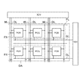
- 第1の画素回路を有し第1の色を表示する第1の画素と、
前記第1の画素に隣接し、第2の画素回路を有し、前記第1の色とは異なる第2の色を表示する第2の画素と、を有する有機EL表示装置であって、
前記第1の画素回路は、
第1の発光領域を備える大発光素子と、
前記第1の発光領域よりも小さい第2の発光領域を備える小発光素子と、
前記小発光素子に電流を供給するか否かと、前記大発光素子に電流を供給するか否かと、前記第1の画素回路が表示する階調に応じて、前記小発光素子と前記大発光素子との一方、或いは両方に供給する前記電流の量とを制御する電流制御回路と、を有し、
前記第2の画素回路は、第3の発光領域を備える発光素子を一つのみ有し、且つ前記発光素子に供給する電流の量を調整する電流調整回路を有し、
前記第1の画素の発光領域は、前記第1の発光領域と前記第2の発光領域とからなり、
前記第2の画素の発光領域は、前記第3の発光領域のみからなり、
前記電流制御回路は、前記階調が閾値以下の場合に前記小発光素子へ前記電流を供給し、前記大発光素子へ前記電流を供給せず、前記階調が前記閾値より大きい場合には、前記大発光素子と前記小発光素子との両方に前記電流を供給する、
ことを特徴とする有機EL表示装置。 - 前記第1の画素回路に含まれる電流制御回路は、前記第1の画素回路が表示する階調が前記閾値より大きい場合に、前記大発光素子に供給する電流の量が、前記階調の増加に応じて単純単調増加するように前記大発光素子に電流を供給する、
ことを特徴とする請求項1に記載の有機EL表示装置。 - 前記電流制御回路は、ソースおよびドレインを含む駆動トランジスタを含み、
前記駆動トランジスタは、前記第1の画素回路が表示する階調に応じて前記小発光素子および前記大発光素子のうち前記電流が供給されるものに供給する電流の量を調節する、
ことを特徴とする請求項1または2に記載の有機EL表示装置。 - 前記大発光素子の一端は、スイッチを介して前記駆動トランジスタのソースおよびドレインのうち一方に接続される、
ことを特徴とする請求項3に記載の有機EL表示装置。 - 前記電流制御回路は、
前記階調が閾値と等しい場合には、前記小発光素子へ第1の電流を供給し、
前記階調が、前記閾値より大きく且つ前記閾値の次の階調である場合は、前記小発光素子へ前記第1の電流よりも小さい第2の電流を供給することを特徴とする請求項1から4のいずれかに記載の有機EL表示装置。 - 前記電流制御回路は、
前記階調が閾値と等しい場合には、前記小発光素子へ第1の電流を供給し、
前記階調が、前記閾値より大きく且つ前記閾値の次の階調である場合は、前記小発光素子へ第2の電流を供給し、
前記第1の電流の電流密度は、前記第2の電流の電流密度よりも大きいことを特徴とする請求項1から4のいずれかに記載の有機EL表示装置。 - 複数のサブ画素を備える画素をさらに有し、
前記第1の画素と前記第2の画素は、前記複数のサブ画素に含まれる、ことを特徴とする請求項1から6のいずれかに記載の有機EL表示装置。 - 前記電流制御回路は、前記階調に応じて前記電流の量を制御する駆動トランジスタを有し、
前記駆動トランジスタのソース電極又はドレイン電極の一方に、前記大発光素子と前記小発光素子とが並列に接続されていることを特徴とする請求項1から7のいずれかに記載の有機EL表示装置。 - 前記一方と前記大発光素子との間には、スイッチが配置されていることを特徴とする請求項8に記載の有機EL表示装置。
- 前記スイッチはトランジスタであり、
前記トランジスタのゲート電極には、前記スイッチへ入力される信号を記憶するメモリ回路が接続されていることを特徴とする請求項9に記載の有機EL表示装置。 - 第1の画素回路を有し第1の色を表示する第1の画素と、
前記第1の画素に隣接し、第2の画素回路を有し、前記第1の色とは異なる第2の色を表示する第2の画素と、を有する有機EL表示装置であって、
前記第1の画素回路は、
第1の発光領域を備える大発光素子と、
前記第1の発光領域よりも小さい第2の発光領域を備える小発光素子と、
前記小発光素子に電流を供給するか否かと、前記大発光素子に電流を供給するか否かと、前記第1の画素回路が表示する階調に応じて、前記小発光素子と前記大発光素子との一方、或いは両方に供給する前記電流の量とを制御する電流制御回路と、を有し、
前記第2の画素回路は、第3の発光領域を備える発光素子を一つのみ有し、且つ前記発光素子に供給する電流の量を調整する電流調整回路を有し、
前記第1の画素の発光領域は、前記第1の発光領域と前記第2の発光領域とからなり、
前記第2の画素の発光領域は、前記第3の発光領域のみからなり、
前記電流制御回路は、前記階調が閾値以下の場合に前記小発光素子へ前記電流を供給し、前記大発光素子へ前記電流を供給せず、前記階調が前記閾値より大きいと共に、前記閾値よりも大きい第2の閾値より小さい場合には、前記大発光素子のみに前記電流を供給し、前記階調が前記第2の閾値より大きい場合には、前記大発光素子と前記小発光素子との両方に前記電流を供給する、
ことを特徴とする有機EL表示装置。 - 前記第1の画素回路に含まれる電流制御回路は、前記第1の画素回路が表示する階調が前記閾値より大きい場合に、前記大発光素子に供給する電流の量が、前記階調の増加に応じて単純単調増加するように前記大発光素子に電流を供給する、
ことを特徴とする請求項11に記載の有機EL表示装置。 - 第1の画素回路を有し第1の色を表示する第1の画素と、
前記第1の画素に隣接し、第2の画素回路を有し、前記第1の色とは異なる第2の色を表示する第2の画素と、を有する有機EL表示装置であって、
前記第1の画素回路は、
第1の発光領域を備える大発光素子と、
前記第1の発光領域よりも小さい第2の発光領域を備える小発光素子と、
前記小発光素子に電流を供給するか否かと、前記大発光素子に電流を供給するか否かと、前記第1の画素回路が表示する階調に応じて、前記小発光素子と前記大発光素子との一方、或いは両方に供給する前記電流の量とを制御する電流制御回路と、を有し、
前記第2の画素回路は、第3の発光領域を備える発光素子を一つのみ有し、且つ前記発光素子に供給する電流の量を調整する電流調整回路を有し、
前記第1の画素の発光領域は、前記第1の発光領域と前記第2の発光領域とからなり、
前記第2の画素の発光領域は、前記第3の発光領域のみからなり、
前記電流制御回路は、前記階調が閾値以下の場合に前記小発光素子へ前記電流を供給し、前記大発光素子へ前記電流を供給せず、前記階調が前記閾値より大きい場合には少なくとも前記大発光素子に前記電流を供給し、
前記電流制御回路は、前記階調に応じて前記電流の量を制御する駆動トランジスタを有し、
前記駆動トランジスタのソース電極又はドレイン電極の一方に、前記大発光素子と前記小発光素子とが並列に接続されている、
ことを特徴とする有機EL表示装置。 - 前記一方と前記大発光素子との間には、スイッチが配置されている、
ことを特徴とする請求項13に記載の有機EL表示装置。 - 前記スイッチはトランジスタであり、
前記トランジスタのゲート電極には、前記スイッチへ入力される信号を記憶するメモリ回路が接続されていることを特徴とする請求項14に記載の有機EL表示装置。 - 前記電流制御回路は、
前記階調が前記閾値より大きいと共に、前記閾値よりも大きい第2の閾値より小さい場合には、前記大発光素子のみに前記電流を供給し、
前記階調が前記第2の閾値より大きい場合には、前記大発光素子と前記小発光素子との両方に前記電流を供給する、
ことを特徴とする請求項13から15のいずれかに記載の有機EL表示装置。
Priority Applications (2)
| Application Number | Priority Date | Filing Date | Title |
|---|---|---|---|
| JP2013243783A JP6285158B2 (ja) | 2013-11-26 | 2013-11-26 | 有機el表示装置 |
| US14/552,519 US9711084B2 (en) | 2013-11-26 | 2014-11-25 | Pixel circuit with large and small OLED elements connected to a single driving transistor wherein the large OLED element is further controlled by a memory circuit within the pixel |
Applications Claiming Priority (1)
| Application Number | Priority Date | Filing Date | Title |
|---|---|---|---|
| JP2013243783A JP6285158B2 (ja) | 2013-11-26 | 2013-11-26 | 有機el表示装置 |
Publications (3)
| Publication Number | Publication Date |
|---|---|
| JP2015102723A JP2015102723A (ja) | 2015-06-04 |
| JP2015102723A5 JP2015102723A5 (ja) | 2016-11-04 |
| JP6285158B2 true JP6285158B2 (ja) | 2018-02-28 |
Family
ID=53182295
Family Applications (1)
| Application Number | Title | Priority Date | Filing Date |
|---|---|---|---|
| JP2013243783A Active JP6285158B2 (ja) | 2013-11-26 | 2013-11-26 | 有機el表示装置 |
Country Status (2)
| Country | Link |
|---|---|
| US (1) | US9711084B2 (ja) |
| JP (1) | JP6285158B2 (ja) |
Cited By (1)
| Publication number | Priority date | Publication date | Assignee | Title |
|---|---|---|---|---|
| WO2022191406A1 (ko) * | 2021-03-10 | 2022-09-15 | 삼성디스플레이 주식회사 | 화소 및 이를 포함하는 표시 장치 |
Families Citing this family (9)
| Publication number | Priority date | Publication date | Assignee | Title |
|---|---|---|---|---|
| JP6932596B2 (ja) | 2017-09-25 | 2021-09-08 | キヤノン株式会社 | 有機el表示装置 |
| JP7114434B2 (ja) * | 2018-10-12 | 2022-08-08 | 日本放送協会 | 画像表示装置、駆動方法及び駆動プログラム |
| WO2020170399A1 (ja) * | 2019-02-21 | 2020-08-27 | シャープ株式会社 | 発光素子及び表示装置 |
| DE102019112456B4 (de) * | 2019-05-13 | 2023-05-25 | OSRAM Opto Semiconductors Gesellschaft mit beschränkter Haftung | Anzeigevorrichtung und betriebsverfahren für eine anzeigevorrichtung |
| JP7316655B2 (ja) * | 2019-10-28 | 2023-07-28 | 株式会社Joled | 画素回路、及び、表示装置 |
| WO2021149237A1 (ja) | 2020-01-24 | 2021-07-29 | シャープ株式会社 | ディスプレイおよびディスプレイの駆動方法 |
| CN111986621B (zh) * | 2020-08-06 | 2022-12-23 | 武汉华星光电半导体显示技术有限公司 | Oled显示面板 |
| WO2022133881A1 (zh) * | 2020-12-24 | 2022-06-30 | 华为技术有限公司 | 一种像素结构和显示面板 |
| WO2024062513A1 (ja) * | 2022-09-20 | 2024-03-28 | シャープディスプレイテクノロジー株式会社 | 表示装置 |
Family Cites Families (22)
| Publication number | Priority date | Publication date | Assignee | Title |
|---|---|---|---|---|
| JP4822590B2 (ja) * | 2001-02-08 | 2011-11-24 | 三洋電機株式会社 | 有機el回路 |
| US6956553B2 (en) * | 2001-04-27 | 2005-10-18 | Sanyo Electric Co., Ltd. | Active matrix display device |
| JP4143323B2 (ja) * | 2002-04-15 | 2008-09-03 | Nec液晶テクノロジー株式会社 | 液晶表示装置 |
| JP2004226673A (ja) | 2003-01-23 | 2004-08-12 | Toyota Industries Corp | 有機電界発光装置 |
| JP4552421B2 (ja) | 2003-11-13 | 2010-09-29 | セイコーエプソン株式会社 | 電気光学装置、電子機器及び電気光学装置の駆動方法 |
| FR2866973B1 (fr) * | 2004-02-27 | 2006-08-04 | Commissariat Energie Atomique | Dispositif ameliore d'adressage de pixels |
| TWI264593B (en) * | 2005-08-12 | 2006-10-21 | Au Optronics Corp | Pixel structure and controlling system thereof |
| JP5132097B2 (ja) * | 2005-07-14 | 2013-01-30 | 株式会社半導体エネルギー研究所 | 表示装置 |
| JP4211800B2 (ja) * | 2006-04-19 | 2009-01-21 | セイコーエプソン株式会社 | 電気光学装置、電気光学装置の駆動方法および電子機器 |
| JP4222396B2 (ja) * | 2006-09-11 | 2009-02-12 | ソニー株式会社 | アクティブマトリクス表示装置 |
| JP2008225101A (ja) * | 2007-03-13 | 2008-09-25 | Fujifilm Corp | 表示装置 |
| JP2008227182A (ja) * | 2007-03-13 | 2008-09-25 | Fujifilm Corp | 表示装置 |
| JP2008268437A (ja) * | 2007-04-18 | 2008-11-06 | Hitachi Displays Ltd | 有機el表示装置 |
| JP2009109521A (ja) * | 2007-10-26 | 2009-05-21 | Sony Corp | 表示装置、表示装置の駆動方法および電子機器 |
| JP2009122401A (ja) * | 2007-11-15 | 2009-06-04 | Toppoly Optoelectronics Corp | アクティブマトリクス型の表示装置 |
| KR101427583B1 (ko) * | 2007-11-16 | 2014-08-08 | 삼성디스플레이 주식회사 | 유기 발광 표시 장치 |
| JP4807366B2 (ja) * | 2008-03-11 | 2011-11-02 | ソニー株式会社 | 表示装置 |
| JP5094685B2 (ja) * | 2008-10-31 | 2012-12-12 | 奇美電子股▲ふん▼有限公司 | アクティブマトリクス型の表示装置及び表示方法 |
| US20110273493A1 (en) * | 2010-05-10 | 2011-11-10 | Chimei Innolux Corporation | Pixel structure and display device having the same |
| JP2012058639A (ja) * | 2010-09-13 | 2012-03-22 | Canon Inc | 有機エレクトロルミネッセンス表示装置とその駆動方法 |
| JP2012113965A (ja) * | 2010-11-25 | 2012-06-14 | Canon Inc | 有機el表示装置 |
| KR20140140968A (ko) * | 2013-05-30 | 2014-12-10 | 삼성디스플레이 주식회사 | 화소, 화소의 구동 방법, 및 화소를 포함하는 표시 장치 |
-
2013
- 2013-11-26 JP JP2013243783A patent/JP6285158B2/ja active Active
-
2014
- 2014-11-25 US US14/552,519 patent/US9711084B2/en active Active
Cited By (2)
| Publication number | Priority date | Publication date | Assignee | Title |
|---|---|---|---|---|
| WO2022191406A1 (ko) * | 2021-03-10 | 2022-09-15 | 삼성디스플레이 주식회사 | 화소 및 이를 포함하는 표시 장치 |
| US11823622B2 (en) | 2021-03-10 | 2023-11-21 | Samsung Display Co., Ltd. | Pixel and display device including the same |
Also Published As
| Publication number | Publication date |
|---|---|
| US20150145906A1 (en) | 2015-05-28 |
| JP2015102723A (ja) | 2015-06-04 |
| US9711084B2 (en) | 2017-07-18 |
Similar Documents
| Publication | Publication Date | Title |
|---|---|---|
| JP6285158B2 (ja) | 有機el表示装置 | |
| US8552636B2 (en) | High resolution pixel architecture | |
| JP4209831B2 (ja) | 表示装置のピクセル回路,表示装置,及びその駆動方法 | |
| US20070176862A1 (en) | Active matrix display with pixel to pixel non-uniformity improvement at low luminance level | |
| US8022907B2 (en) | Brightness controlled organic light emitting display and method of driving the same | |
| US8228270B2 (en) | Display device and driving method thereof | |
| JP6192431B2 (ja) | 有機el表示装置の駆動方法、及び有機el表示装置 | |
| US20060221014A1 (en) | Organic light emitting display and method of driving the same | |
| JP5015714B2 (ja) | 画素回路 | |
| JP2005148750A (ja) | 表示装置のピクセル回路,表示装置,及びその駆動方法 | |
| US20060077195A1 (en) | Image display device | |
| KR20080082279A (ko) | 유기전계발광표시장치 및 그의 제조방법 | |
| US10971050B2 (en) | Method for driving a display panel to display image, display apparatus thereof, and driver enabled to perform the method | |
| WO2019186874A1 (ja) | 表示デバイスおよび駆動方法 | |
| JP2019211564A (ja) | 表示装置及びその制御方法 | |
| KR102483946B1 (ko) | 유기발광표시장치 및 그의 구동방법 | |
| JP2005032704A (ja) | 表示素子および表示装置 | |
| JP2012118381A (ja) | 有機el表示装置及びその駆動方法 | |
| JP2007114285A (ja) | 表示装置及びその駆動方法 | |
| CN110556074B (zh) | 显示装置以及控制该显示装置的方法 | |
| JP2019045820A (ja) | 表示装置 | |
| JP7455521B2 (ja) | 表示制御装置、表示装置及び表示制御方法 | |
| JP5636158B2 (ja) | 画像表示装置 | |
| US20120105499A1 (en) | Light-emitting element display device | |
| JP2005301176A (ja) | 表示装置 |
Legal Events
| Date | Code | Title | Description |
|---|---|---|---|
| A521 | Request for written amendment filed |
Free format text: JAPANESE INTERMEDIATE CODE: A523 Effective date: 20160914 |
|
| A621 | Written request for application examination |
Free format text: JAPANESE INTERMEDIATE CODE: A621 Effective date: 20160914 |
|
| A977 | Report on retrieval |
Free format text: JAPANESE INTERMEDIATE CODE: A971007 Effective date: 20170626 |
|
| A131 | Notification of reasons for refusal |
Free format text: JAPANESE INTERMEDIATE CODE: A131 Effective date: 20170718 |
|
| A521 | Request for written amendment filed |
Free format text: JAPANESE INTERMEDIATE CODE: A523 Effective date: 20170830 |
|
| TRDD | Decision of grant or rejection written | ||
| A01 | Written decision to grant a patent or to grant a registration (utility model) |
Free format text: JAPANESE INTERMEDIATE CODE: A01 Effective date: 20180130 |
|
| A61 | First payment of annual fees (during grant procedure) |
Free format text: JAPANESE INTERMEDIATE CODE: A61 Effective date: 20180201 |
|
| R150 | Certificate of patent or registration of utility model |
Ref document number: 6285158 Country of ref document: JP Free format text: JAPANESE INTERMEDIATE CODE: R150 |
|
| R250 | Receipt of annual fees |
Free format text: JAPANESE INTERMEDIATE CODE: R250 |
|
| R250 | Receipt of annual fees |
Free format text: JAPANESE INTERMEDIATE CODE: R250 |
|
| R250 | Receipt of annual fees |
Free format text: JAPANESE INTERMEDIATE CODE: R250 |
|
| R250 | Receipt of annual fees |
Free format text: JAPANESE INTERMEDIATE CODE: R250 |