JP6239525B2 - Igbtのターンオフ過電圧の制限 - Google Patents
Igbtのターンオフ過電圧の制限 Download PDFInfo
- Publication number
- JP6239525B2 JP6239525B2 JP2014545054A JP2014545054A JP6239525B2 JP 6239525 B2 JP6239525 B2 JP 6239525B2 JP 2014545054 A JP2014545054 A JP 2014545054A JP 2014545054 A JP2014545054 A JP 2014545054A JP 6239525 B2 JP6239525 B2 JP 6239525B2
- Authority
- JP
- Japan
- Prior art keywords
- igbt
- emitter
- power converter
- collector
- parasitic inductance
- Prior art date
- Legal status (The legal status is an assumption and is not a legal conclusion. Google has not performed a legal analysis and makes no representation as to the accuracy of the status listed.)
- Expired - Fee Related
Links
Images


Classifications
-
- H—ELECTRICITY
- H02—GENERATION; CONVERSION OR DISTRIBUTION OF ELECTRIC POWER
- H02M—APPARATUS FOR CONVERSION BETWEEN AC AND AC, BETWEEN AC AND DC, OR BETWEEN DC AND DC, AND FOR USE WITH MAINS OR SIMILAR POWER SUPPLY SYSTEMS; CONVERSION OF DC OR AC INPUT POWER INTO SURGE OUTPUT POWER; CONTROL OR REGULATION THEREOF
- H02M7/00—Conversion of AC power input into DC power output; Conversion of DC power input into AC power output
- H02M7/42—Conversion of DC power input into AC power output without possibility of reversal
- H02M7/44—Conversion of DC power input into AC power output without possibility of reversal by static converters
- H02M7/48—Conversion of DC power input into AC power output without possibility of reversal by static converters using discharge tubes with control electrode or semiconductor devices with control electrode
- H02M7/53—Conversion of DC power input into AC power output without possibility of reversal by static converters using discharge tubes with control electrode or semiconductor devices with control electrode using devices of a triode or transistor type requiring continuous application of a control signal
- H02M7/537—Conversion of DC power input into AC power output without possibility of reversal by static converters using discharge tubes with control electrode or semiconductor devices with control electrode using devices of a triode or transistor type requiring continuous application of a control signal using semiconductor devices only, e.g. single switched pulse inverters
-
- H—ELECTRICITY
- H02—GENERATION; CONVERSION OR DISTRIBUTION OF ELECTRIC POWER
- H02M—APPARATUS FOR CONVERSION BETWEEN AC AND AC, BETWEEN AC AND DC, OR BETWEEN DC AND DC, AND FOR USE WITH MAINS OR SIMILAR POWER SUPPLY SYSTEMS; CONVERSION OF DC OR AC INPUT POWER INTO SURGE OUTPUT POWER; CONTROL OR REGULATION THEREOF
- H02M1/00—Details of apparatus for conversion
- H02M1/08—Circuits specially adapted for the generation of control voltages for semiconductor devices incorporated in static converters
-
- H—ELECTRICITY
- H02—GENERATION; CONVERSION OR DISTRIBUTION OF ELECTRIC POWER
- H02M—APPARATUS FOR CONVERSION BETWEEN AC AND AC, BETWEEN AC AND DC, OR BETWEEN DC AND DC, AND FOR USE WITH MAINS OR SIMILAR POWER SUPPLY SYSTEMS; CONVERSION OF DC OR AC INPUT POWER INTO SURGE OUTPUT POWER; CONTROL OR REGULATION THEREOF
- H02M1/00—Details of apparatus for conversion
- H02M1/32—Means for protecting converters other than automatic disconnection
-
- H—ELECTRICITY
- H03—ELECTRONIC CIRCUITRY
- H03K—PULSE TECHNIQUE
- H03K17/00—Electronic switching or gating, i.e. not by contact-making and –breaking
- H03K17/08—Modifications for protecting switching circuit against overcurrent or overvoltage
- H03K17/082—Modifications for protecting switching circuit against overcurrent or overvoltage by feedback from the output to the control circuit
- H03K17/0828—Modifications for protecting switching circuit against overcurrent or overvoltage by feedback from the output to the control circuit in composite switches
-
- H—ELECTRICITY
- H03—ELECTRONIC CIRCUITRY
- H03K—PULSE TECHNIQUE
- H03K17/00—Electronic switching or gating, i.e. not by contact-making and –breaking
- H03K17/16—Modifications for eliminating interference voltages or currents
- H03K17/161—Modifications for eliminating interference voltages or currents in field-effect transistor switches
- H03K17/165—Modifications for eliminating interference voltages or currents in field-effect transistor switches by feedback from the output circuit to the control circuit
- H03K17/166—Soft switching
-
- H—ELECTRICITY
- H03—ELECTRONIC CIRCUITRY
- H03K—PULSE TECHNIQUE
- H03K17/00—Electronic switching or gating, i.e. not by contact-making and –breaking
- H03K17/51—Electronic switching or gating, i.e. not by contact-making and –breaking characterised by the components used
- H03K17/56—Electronic switching or gating, i.e. not by contact-making and –breaking characterised by the components used by the use, as active elements, of semiconductor devices
- H03K17/60—Electronic switching or gating, i.e. not by contact-making and –breaking characterised by the components used by the use, as active elements, of semiconductor devices the devices being bipolar transistors
-
- H—ELECTRICITY
- H02—GENERATION; CONVERSION OR DISTRIBUTION OF ELECTRIC POWER
- H02M—APPARATUS FOR CONVERSION BETWEEN AC AND AC, BETWEEN AC AND DC, OR BETWEEN DC AND DC, AND FOR USE WITH MAINS OR SIMILAR POWER SUPPLY SYSTEMS; CONVERSION OF DC OR AC INPUT POWER INTO SURGE OUTPUT POWER; CONTROL OR REGULATION THEREOF
- H02M1/00—Details of apparatus for conversion
- H02M1/0003—Details of control, feedback or regulation circuits
- H02M1/0029—Circuits or arrangements for limiting the slope of switching signals, e.g. slew rate
-
- H—ELECTRICITY
- H10—SEMICONDUCTOR DEVICES; ELECTRIC SOLID-STATE DEVICES NOT OTHERWISE PROVIDED FOR
- H10W—GENERIC PACKAGES, INTERCONNECTIONS, CONNECTORS OR OTHER CONSTRUCTIONAL DETAILS OF DEVICES COVERED BY CLASS H10
- H10W72/00—Interconnections or connectors in packages
- H10W72/50—Bond wires
- H10W72/541—Dispositions of bond wires
- H10W72/547—Dispositions of multiple bond wires
- H10W72/5475—Dispositions of multiple bond wires multiple bond wires connected to common bond pads at both ends of the wires
Landscapes
- Engineering & Computer Science (AREA)
- Power Engineering (AREA)
- Power Conversion In General (AREA)
- Electronic Switches (AREA)
- Inverter Devices (AREA)
Description
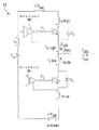
直列に接続され、第1のIGBTのエミッタの寄生インダクタンスに接続される第1および第2の抵抗器であり、第1のIGBTのゲートドライバリファレンスが第1の抵抗器と第2の抵抗器との間の接続ポイントに接続される第1および第2の抵抗器と、
第2のIGBTのコレクタの寄生インダクタンスに接続される1次巻線と第2のIGBTのエミッタの寄生インダクタンスに接続される2次巻線とを有するトランスと、を含み、第2のIGBTのゲートドライバのリファレンスは、トランスの2次巻線に接続される。
直列に接続され、第1のIGBTのエミッタの寄生インダクタンスに接続される第1および第2の抵抗器であり、第1のIGBTのゲートドライバリファレンスが第1の抵抗器と第2の抵抗器との間の接続ポイントに接続される第1および第2の抵抗器と、
第2のIGBTのコレクタの寄生インダクタンスに接続される1次巻線、および第2のIGBTのエミッタの寄生インダクタンスに直列に接続される2次巻線を有するトランスと、を含み、第2のIGBTのゲートドライバリファレンスは、トランスの2次巻線に接続される。
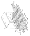
12 三相電力コンバータ
14 コレクタ
16 エミッタ
18 ゲート
20 ゲートドライバ
22 リファレンス
24 平坦部分
102 IGBT
104 トレース
106 エミッタパッド
110 ワイヤボンド
112 IGBT
114 トレース
116 コレクタパッド
118 トレース
120 ワイヤボンド
126 位相タブ
128 U字形のコネクタ
130 脚部
132 より大きなコネクタ
Claims (15)
- ゲート、コレクタおよびエミッタを各々有する第1および第2のIGBTと、前記第2のIGBTのコレクタの寄生インダクタンスに接続される1次巻線、および2次巻線を有するトランスとを含むDC−AC電力コンバータであって、前記各IGBTの前記ゲートは、リファレンスを含むゲートドライバに接続され、前記第1のIGBTのゲートドライバリファレンスは、前記電力コンバータの接地バスに接続され、前記第2のIGBTのゲートドライバリファレンスは、前記トランスの2次巻線を介して前記第1のIGBTの前記コレクタに接続され、前記第2のIGBTの前記エミッタの寄生インダクタンスは、前記トランスの2次巻線によって、前記第2のIGBTのターンオフにおける過電圧を制限する制御を可能にするように増加するDC−AC電力コンバータ。
- 各IGBTについて、前記ゲートドライバは、直列に接続され、前記対応するIGBTの前記エミッタの寄生インダクタンスに接続される第1および第2の抵抗器を含み、前記ゲートドライバリファレンスは、前記第1の抵抗器と前記第2の抵抗器との間の接続ポイントに接続される、請求項1に記載のDC−AC電力コンバータ。
- 前記トランスの2次巻線は、前記第2のIGBTの前記エミッタの前記寄生インダクタンスならびに第1および第2の抵抗器に直列に接続されている、請求項1に記載のDC−AC電力コンバータ。
- 前記第2のIGBTの前記エミッタと前記第1のIGBTの前記コレクタとの間にコネクタを設けることによって、前記第2のIGBTの前記エミッタの前記寄生インダクタンスが増加し、前記コネクタは、増加された等価な寄生インダクタンスを与えるように構成される、請求項1に記載のDC−AC電力コンバータ。
- 前記第2のIGBTの前記エミッタはエミッタパッドに接続され、前記第1のIGBTの前記コレクタはコレクタパッドに接続され、前記コネクタは、前記エミッタパッドと前記コレクタパッドとの間に設けられる、請求項4に記載のDC−AC電力コンバータ。
- 前記エミッタパッドは複数のエミッタパッドを含み、前記コレクタパッドは複数のコレクタパッドを含む、請求項5に記載のDC−AC電力コンバータ。
- 前記コネクタはU字形の断面を有する、請求項5に記載のDC−AC電力コンバータ。
- 前記U字形のコネクタは、前記パッドと相互接続するように構成される脚部を含む、請求項7に記載のDC−AC電力コンバータ。
- コレクタ、エミッタ、ゲートおよびリファレンスを含むゲートドライバを有する第1のIGBTと、コレクタ、エミッタ、ゲートおよびリファレンスを含むゲートドライバを有する第2のIGBTと、を含むDC−AC電力コンバータであって、前記電力コンバータは、
直列に接続され、前記第1のIGBTの前記エミッタの寄生インダクタンスに接続される第1および第2の抵抗器であり、前記第1のIGBTのゲートドライバリファレンスが前記第1の抵抗器と前記第2の抵抗器との間の接続ポイントに接続される第1および第2の抵抗器と、
前記第2のIGBTの前記コレクタの前記寄生インダクタンスに接続される1次巻線と前記第2のIGBTの前記エミッタの前記寄生インダクタンスに接続される2次巻線とを有するトランスと、を含み、前記第2のIGBTの前記ゲートドライバの前記リファレンスは、前記トランスの前記2次巻線に接続されるDC−AC電力コンバータ。 - 前記ゲートドライバリファレンスは、第3の抵抗を介して前記トランスの前記2次巻線に接続される、請求項9に記載のDC−AC電力コンバータ。
- コレクタ、エミッタ、ゲートおよびリファレンスを含むゲートドライバを有する第1のIGBTと、コレクタ、エミッタ、ゲートおよびリファレンスを含むゲートドライバを有する第2のIGBTと、を含むDC−AC電力コンバータであって、前記電力コンバータは、
直列に接続され、前記第1のIGBTの前記エミッタの寄生インダクタンスに接続される第1および第2の抵抗器であり、前記第1のIGBTのゲートドライバリファレンスが前記第1の抵抗器と前記第2の抵抗器との間の接続ポイントに接続される第1および第2の抵抗器と、
前記第2のIGBTの前記コレクタの前記寄生インダクタンスに接続される1次巻線、および前記第2のIGBTの前記エミッタの前記寄生インダクタンスに直列に接続される2次巻線を有するトランスと、を含み、前記第2のIGBTのゲートドライバリファレンスは、前記トランスの前記2次巻線に接続されるDC−AC電力コンバータ。 - 前記トランスの前記2次巻線は、前記第2のIGBTの前記エミッタの前記寄生インダクタンスならびに第3および第4の抵抗器の両方と直列に接続され、前記第2のIGBTの前記ゲートドライバリファレンスは、前記第3の抵抗器と前記第4の抵抗器との間の接続ポイントに接続される、請求項11に記載のDC−AC電力コンバータ。
- 前記トランスの前記2次巻線は、前記第2のIGBTの前記エミッタの前記寄生インダクタンス、前記第1のIGBTの前記コレクタの前記寄生インダクタンス、ならびに前記第3および前記第4の抵抗器に直列に接続される、請求項12に記載のDC−AC電力コンバータ。
- 高周波ループを含むDC−AC電力コンバータであって、前記高周波ループは、
ゲート、コレクタおよびエミッタを各々有する下部IGBTおよび上部IGBTであり、前記各IGBTの前記ゲートがリファレンスを含むゲートドライバに接続され、前記下部IGBTのゲートドライバリファレンスは、前記電力コンバータの接地バスに接続され、前記上部IGBTのゲートドライバリファレンスは、前記下部IGBTの前記コレクタに接続される、下部IGBTおよび上部IGBTと、
前記高周波ループの様々な素子の相互接続によって定義される寄生インダクタンスと、を有し、前記上部IGBTの前記エミッタの、および前記下部IGBTの前記コレクタの前記寄生インダクタンスは、前記高周波ループの前記寄生インダクタンスの一部であり、
前記高周波ループの前記寄生インダクタンスで誘起された電圧の一部は、トランスによって、前記上部IGBTの前記エミッタの、および前記下部IGBTの前記コレクタの寄生インダクタンスで誘起された電圧に付加されて、前記上部IGBTのゲート−エミッタ電圧(Vge)の勾配を緩やかにし、前記トランスは、前記高周波ループの寄生インダクタンスに接続される1次巻線、および前記上部IGBTの前記エミッタの前記寄生インダクタンスと直列に前記上部IGBTの前記ゲートドライバに接続される2次巻線を有している、
DC−AC電力コンバータ。 - 各IGBTについて、前記ゲートドライバは、直列に接続され、前記対応するIGBTの前記エミッタの寄生インダクタンスに接続される第1および第2の抵抗器を含み、前記ゲートドライバリファレンスは、前記第1の抵抗器と前記第2の抵抗器との間の接続ポイントに接続される、請求項14に記載のDC−AC電力コンバータ。
Applications Claiming Priority (3)
| Application Number | Priority Date | Filing Date | Title |
|---|---|---|---|
| US201161567800P | 2011-12-07 | 2011-12-07 | |
| US61/567,800 | 2011-12-07 | ||
| PCT/CA2012/001125 WO2013082705A1 (en) | 2011-12-07 | 2012-12-05 | Turn-off overvoltage limiting for igbt |
Publications (2)
| Publication Number | Publication Date |
|---|---|
| JP2015503319A JP2015503319A (ja) | 2015-01-29 |
| JP6239525B2 true JP6239525B2 (ja) | 2017-11-29 |
Family
ID=48573450
Family Applications (1)
| Application Number | Title | Priority Date | Filing Date |
|---|---|---|---|
| JP2014545054A Expired - Fee Related JP6239525B2 (ja) | 2011-12-07 | 2012-12-05 | Igbtのターンオフ過電圧の制限 |
Country Status (8)
| Country | Link |
|---|---|
| US (2) | US9608543B2 (ja) |
| EP (1) | EP2789092B1 (ja) |
| JP (1) | JP6239525B2 (ja) |
| CN (1) | CN103988410B (ja) |
| BR (1) | BR112014012206A2 (ja) |
| CA (1) | CA2851376C (ja) |
| IN (1) | IN2014DN03024A (ja) |
| WO (1) | WO2013082705A1 (ja) |
Families Citing this family (16)
| Publication number | Priority date | Publication date | Assignee | Title |
|---|---|---|---|---|
| CN103988410B (zh) * | 2011-12-07 | 2017-10-13 | Tm4股份有限公司 | 用于绝缘栅双极型晶体管的关断过电压限制 |
| US9112501B2 (en) * | 2012-09-29 | 2015-08-18 | Infineon Technologies Ag | Electronic circuit with an electronic switch and a monitoring circuit |
| CA2907472C (en) | 2013-04-04 | 2017-05-02 | Tm4 Inc. | Commutation cell and compensation circuit therefor |
| US9774244B2 (en) | 2013-11-01 | 2017-09-26 | Tm4 Inc. | Power converter configured for limiting switching overvoltage |
| CA2930187A1 (en) * | 2013-11-14 | 2015-05-21 | Tm4 Inc. | Commutation cell, power converter and compensation circuit having dynamically controlled voltage gains |
| WO2015070344A1 (en) | 2013-11-14 | 2015-05-21 | Tm4 Inc. | Compensation circuit, commutation cell and power converter controlling turn-on and turn-off of a power electronic switch |
| CA2989672C (en) | 2015-06-23 | 2022-11-29 | Tm4 Inc. | Physical topology for a power converter |
| US9812941B2 (en) | 2015-09-11 | 2017-11-07 | Nxp Usa, Inc. | High power driver having multiple turn off modes |
| WO2017045071A1 (en) * | 2015-09-14 | 2017-03-23 | Tm4 Inc. | Power converter configured for limiting switching overvoltage |
| CN107154791A (zh) * | 2016-03-02 | 2017-09-12 | 国网辽宁省电力有限公司电力科学研究院 | 高压大功率igbt模块的电流上升斜率检测电路及其检测方法 |
| US10122294B2 (en) | 2016-12-01 | 2018-11-06 | Ford Global Technologies, Llc | Active gate clamping for inverter switching devices with enhanced common source inductance |
| US9866099B1 (en) * | 2016-12-30 | 2018-01-09 | Texas Instruments Incorporated | Adaptive high-side gate drive for ringing mitigation in switching power converters |
| JP7341885B2 (ja) * | 2019-12-27 | 2023-09-11 | 川崎重工業株式会社 | スイッチング回路 |
| DE112021007336T5 (de) * | 2021-03-19 | 2023-12-28 | Mitsubishi Electric Corporation | Gleichstromversorgung, Kältekreislaufvorrichtung, Klimatisierungsvorrichtung und Kühlvorrichtung |
| WO2023001995A1 (fr) * | 2021-07-21 | 2023-01-26 | Valeo Systemes De Controle Moteur | Systeme de commutation et convertisseur de tension ou engin de mobilite comprenant un tel systeme de commutation |
| US12531554B2 (en) | 2023-02-27 | 2026-01-20 | Rtx Corporation | Enhanced solid state circuit breaker structure |
Family Cites Families (23)
| Publication number | Priority date | Publication date | Assignee | Title |
|---|---|---|---|---|
| JP3379556B2 (ja) * | 1993-12-30 | 2003-02-24 | サンケン電気株式会社 | スイッチング素子を有する回路装置 |
| KR100337035B1 (ko) * | 1999-11-26 | 2002-05-16 | 권영한 | 전력용 반도체 스위칭 소자의 직렬구동을 위한 수동형보조회로 |
| JP3598933B2 (ja) | 2000-02-28 | 2004-12-08 | 株式会社日立製作所 | 電力変換装置 |
| JP3932841B2 (ja) * | 2001-08-29 | 2007-06-20 | 株式会社日立製作所 | 半導体電力変換装置 |
| JP3731562B2 (ja) * | 2002-05-22 | 2006-01-05 | 日産自動車株式会社 | 電流制御型素子用駆動回路 |
| DE10231198A1 (de) * | 2002-07-10 | 2004-01-29 | eupec Europäische Gesellschaft für Leistungshalbleiter mbH | Verfahren und Schaltungsanordnung zum Begrenzen einer Überspannung |
| JP3975162B2 (ja) * | 2002-12-20 | 2007-09-12 | トヨタ自動車株式会社 | インバータ装置およびそれを用いた電動機一体インバータ装置 |
| JP4739059B2 (ja) | 2006-02-23 | 2011-08-03 | ルネサスエレクトロニクス株式会社 | Dc/dcコンバータ用半導体装置 |
| JP4432953B2 (ja) * | 2006-09-27 | 2010-03-17 | 株式会社日立製作所 | 半導体電力変換装置 |
| EP2434627A4 (en) * | 2009-05-19 | 2014-07-02 | Mitsubishi Electric Corp | GATE DRIVE CIRCUIT |
| US8149600B2 (en) | 2009-05-22 | 2012-04-03 | Infineon Technologies Ag | System and method for ringing suppression in a switched mode power supply |
| JP5315155B2 (ja) * | 2009-07-23 | 2013-10-16 | 日立オートモティブシステムズ株式会社 | 半導体素子制御装置、車載用電機システム |
| EP2526616A2 (en) | 2010-01-22 | 2012-11-28 | Massachusetts Institute of Technology | Grid-tied power conversion circuits and related techniques |
| KR101449083B1 (ko) * | 2010-05-06 | 2014-10-13 | 엘에스산전 주식회사 | 스위칭 게이트 드라이브 |
| US9793889B2 (en) * | 2011-03-15 | 2017-10-17 | Infineon Technologies Ag | Semiconductor device including a circuit to compensate for parasitic inductance |
| CN103988410B (zh) * | 2011-12-07 | 2017-10-13 | Tm4股份有限公司 | 用于绝缘栅双极型晶体管的关断过电压限制 |
| WO2013138219A1 (en) * | 2012-03-12 | 2013-09-19 | Board Of Trustees Of Michigan State University | High efficiency gate drive circuit for power transistors |
| WO2014043795A1 (en) * | 2012-09-24 | 2014-03-27 | Tm4 Inc. | Topology for controlled power switch module |
| CA2907472C (en) * | 2013-04-04 | 2017-05-02 | Tm4 Inc. | Commutation cell and compensation circuit therefor |
| US9774244B2 (en) * | 2013-11-01 | 2017-09-26 | Tm4 Inc. | Power converter configured for limiting switching overvoltage |
| CA2930187A1 (en) * | 2013-11-14 | 2015-05-21 | Tm4 Inc. | Commutation cell, power converter and compensation circuit having dynamically controlled voltage gains |
| WO2015070344A1 (en) * | 2013-11-14 | 2015-05-21 | Tm4 Inc. | Compensation circuit, commutation cell and power converter controlling turn-on and turn-off of a power electronic switch |
| US9608620B2 (en) * | 2013-12-03 | 2017-03-28 | Ingeteam Power Technology, S.A. | Control system and control method for controlling a switching device integrated in an electronic converter and switching cell comprising said system |
-
2012
- 2012-12-05 CN CN201280060186.9A patent/CN103988410B/zh active Active
- 2012-12-05 US US14/363,439 patent/US9608543B2/en active Active
- 2012-12-05 EP EP12856190.9A patent/EP2789092B1/en active Active
- 2012-12-05 CA CA2851376A patent/CA2851376C/en active Active
- 2012-12-05 BR BR112014012206A patent/BR112014012206A2/pt not_active IP Right Cessation
- 2012-12-05 WO PCT/CA2012/001125 patent/WO2013082705A1/en not_active Ceased
- 2012-12-05 JP JP2014545054A patent/JP6239525B2/ja not_active Expired - Fee Related
- 2012-12-05 IN IN3024DEN2014 patent/IN2014DN03024A/en unknown
-
2017
- 2017-02-13 US US15/431,418 patent/US10205405B2/en active Active
Also Published As
| Publication number | Publication date |
|---|---|
| US9608543B2 (en) | 2017-03-28 |
| WO2013082705A1 (en) | 2013-06-13 |
| CN103988410B (zh) | 2017-10-13 |
| BR112014012206A2 (pt) | 2017-05-30 |
| CA2851376C (en) | 2021-02-16 |
| JP2015503319A (ja) | 2015-01-29 |
| IN2014DN03024A (ja) | 2015-05-08 |
| US20170163172A1 (en) | 2017-06-08 |
| CA2851376A1 (en) | 2013-06-13 |
| CN103988410A (zh) | 2014-08-13 |
| US20140321178A1 (en) | 2014-10-30 |
| EP2789092B1 (en) | 2020-02-05 |
| EP2789092A4 (en) | 2016-05-04 |
| EP2789092A1 (en) | 2014-10-15 |
| US10205405B2 (en) | 2019-02-12 |
Similar Documents
| Publication | Publication Date | Title |
|---|---|---|
| JP6239525B2 (ja) | Igbtのターンオフ過電圧の制限 | |
| JP6611191B2 (ja) | 整流セルおよびそのための補償回路 | |
| US9812987B2 (en) | Topology for controlled power switch module | |
| CN102856308B (zh) | 功率半导体模块 | |
| CN105814781B (zh) | 换向单元、电力变换器和具有动态控制的电压增益的补偿电路 | |
| US9479157B2 (en) | Electric device including a switch circuit, a current limit circuit and a clamp swith, for driving a power switch | |
| US10277112B2 (en) | Physical topology for a power converter | |
| JP6556712B2 (ja) | スイッチング過電圧を制限するように構成された電力変換器 | |
| CN101814854A (zh) | 半导体开关装置 | |
| CN105814780A (zh) | 控制功率电子开关的接通和关断的补偿电路、整流单元和功率转换器 | |
| JP2019068661A (ja) | 半導体装置 | |
| JP2015226067A (ja) | パワーモジュール | |
| KR101301221B1 (ko) | 3상 모터 드라이브용 전력회로 및 3상 모터 드라이브용 전력모듈 | |
| HK1227559A1 (en) | Commutation cell, power converter and compensation circuit having dynamically controlled voltage gains | |
| JP2016005324A (ja) | インバータ回路 |
Legal Events
| Date | Code | Title | Description |
|---|---|---|---|
| A621 | Written request for application examination |
Free format text: JAPANESE INTERMEDIATE CODE: A621 Effective date: 20151118 |
|
| A977 | Report on retrieval |
Free format text: JAPANESE INTERMEDIATE CODE: A971007 Effective date: 20161227 |
|
| A131 | Notification of reasons for refusal |
Free format text: JAPANESE INTERMEDIATE CODE: A131 Effective date: 20170124 |
|
| A521 | Request for written amendment filed |
Free format text: JAPANESE INTERMEDIATE CODE: A523 Effective date: 20170424 |
|
| TRDD | Decision of grant or rejection written | ||
| A01 | Written decision to grant a patent or to grant a registration (utility model) |
Free format text: JAPANESE INTERMEDIATE CODE: A01 Effective date: 20171003 |
|
| A61 | First payment of annual fees (during grant procedure) |
Free format text: JAPANESE INTERMEDIATE CODE: A61 Effective date: 20171101 |
|
| R150 | Certificate of patent or registration of utility model |
Ref document number: 6239525 Country of ref document: JP Free format text: JAPANESE INTERMEDIATE CODE: R150 |
|
| RD02 | Notification of acceptance of power of attorney |
Free format text: JAPANESE INTERMEDIATE CODE: A7422 Effective date: 20190408 |
|
| RD02 | Notification of acceptance of power of attorney |
Free format text: JAPANESE INTERMEDIATE CODE: R3D02 |
|
| LAPS | Cancellation because of no payment of annual fees |