JP6230328B2 - 有機el表示装置 - Google Patents
有機el表示装置 Download PDFInfo
- Publication number
- JP6230328B2 JP6230328B2 JP2013168995A JP2013168995A JP6230328B2 JP 6230328 B2 JP6230328 B2 JP 6230328B2 JP 2013168995 A JP2013168995 A JP 2013168995A JP 2013168995 A JP2013168995 A JP 2013168995A JP 6230328 B2 JP6230328 B2 JP 6230328B2
- Authority
- JP
- Japan
- Prior art keywords
- organic
- light emitting
- display device
- region
- pixels
- Prior art date
- Legal status (The legal status is an assumption and is not a legal conclusion. Google has not performed a legal analysis and makes no representation as to the accuracy of the status listed.)
- Active
Links
Images


Classifications
-
- H—ELECTRICITY
- H10—SEMICONDUCTOR DEVICES; ELECTRIC SOLID-STATE DEVICES NOT OTHERWISE PROVIDED FOR
- H10K—ORGANIC ELECTRIC SOLID-STATE DEVICES
- H10K59/00—Integrated devices, or assemblies of multiple devices, comprising at least one organic light-emitting element covered by group H10K50/00
- H10K59/80—Constructional details
- H10K59/8791—Arrangements for improving contrast, e.g. preventing reflection of ambient light
- H10K59/8792—Arrangements for improving contrast, e.g. preventing reflection of ambient light comprising light absorbing layers, e.g. black layers
-
- H—ELECTRICITY
- H10—SEMICONDUCTOR DEVICES; ELECTRIC SOLID-STATE DEVICES NOT OTHERWISE PROVIDED FOR
- H10K—ORGANIC ELECTRIC SOLID-STATE DEVICES
- H10K50/00—Organic light-emitting devices
- H10K50/80—Constructional details
- H10K50/86—Arrangements for improving contrast, e.g. preventing reflection of ambient light
- H10K50/865—Arrangements for improving contrast, e.g. preventing reflection of ambient light comprising light absorbing layers, e.g. light-blocking layers
-
- H—ELECTRICITY
- H10—SEMICONDUCTOR DEVICES; ELECTRIC SOLID-STATE DEVICES NOT OTHERWISE PROVIDED FOR
- H10K—ORGANIC ELECTRIC SOLID-STATE DEVICES
- H10K59/00—Integrated devices, or assemblies of multiple devices, comprising at least one organic light-emitting element covered by group H10K50/00
- H10K59/10—OLED displays
- H10K59/12—Active-matrix OLED [AMOLED] displays
- H10K59/122—Pixel-defining structures or layers, e.g. banks
-
- H—ELECTRICITY
- H10—SEMICONDUCTOR DEVICES; ELECTRIC SOLID-STATE DEVICES NOT OTHERWISE PROVIDED FOR
- H10K—ORGANIC ELECTRIC SOLID-STATE DEVICES
- H10K59/00—Integrated devices, or assemblies of multiple devices, comprising at least one organic light-emitting element covered by group H10K50/00
- H10K59/30—Devices specially adapted for multicolour light emission
- H10K59/35—Devices specially adapted for multicolour light emission comprising red-green-blue [RGB] subpixels
- H10K59/351—Devices specially adapted for multicolour light emission comprising red-green-blue [RGB] subpixels comprising more than three subpixels, e.g. red-green-blue-white [RGBW]
-
- H—ELECTRICITY
- H10—SEMICONDUCTOR DEVICES; ELECTRIC SOLID-STATE DEVICES NOT OTHERWISE PROVIDED FOR
- H10K—ORGANIC ELECTRIC SOLID-STATE DEVICES
- H10K59/00—Integrated devices, or assemblies of multiple devices, comprising at least one organic light-emitting element covered by group H10K50/00
- H10K59/30—Devices specially adapted for multicolour light emission
- H10K59/35—Devices specially adapted for multicolour light emission comprising red-green-blue [RGB] subpixels
- H10K59/353—Devices specially adapted for multicolour light emission comprising red-green-blue [RGB] subpixels characterised by the geometrical arrangement of the RGB subpixels
-
- H—ELECTRICITY
- H10—SEMICONDUCTOR DEVICES; ELECTRIC SOLID-STATE DEVICES NOT OTHERWISE PROVIDED FOR
- H10K—ORGANIC ELECTRIC SOLID-STATE DEVICES
- H10K59/00—Integrated devices, or assemblies of multiple devices, comprising at least one organic light-emitting element covered by group H10K50/00
- H10K59/30—Devices specially adapted for multicolour light emission
- H10K59/38—Devices specially adapted for multicolour light emission comprising colour filters or colour changing media [CCM]
Landscapes
- Physics & Mathematics (AREA)
- Optics & Photonics (AREA)
- Electroluminescent Light Sources (AREA)
- Devices For Indicating Variable Information By Combining Individual Elements (AREA)
Description
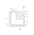
前記複数の長辺はそれぞれ、平面的に見て前記遮光膜と重畳し、前記複数の短辺はそれぞれ、平面的に見て前記遮光膜から露出している、ことを特徴とする有機EL表示装置である。
Claims (6)
- 基板上にマトリクス状に配置された複数の画素と、
前記複数の画素の境界を遮光する遮光膜と、
前記複数の画素のそれぞれにおいて、下部電極及び上部電極の間に配置され、発光する有機材料からなる発光層を含む複数の層からなる有機層が、前記下部電極と接触している領域である発光領域と、を備え、
前記発光領域は、前記複数の画素のそれぞれにおいて、前記画素の形状の辺に沿って延びると共に、互いに平行でない複数の長辺及び、前記複数の長辺よりも短く、互いに平行でない複数の短辺を有し、
前記遮光膜は、前記画素の辺に沿って配置され、互いに幅の異なる幅広部及び幅狭部を有し、
前記幅広部は、前記複数の長辺に対応する前記画素の辺に沿って配置され、前記幅狭部は、前記複数の短辺に対応する前記画素の辺に沿って配置され、
前記複数の長辺はそれぞれ、平面的に見て前記遮光膜と重畳し、前記複数の短辺はそれぞれ、平面的に見て前記遮光膜から露出している、ことを特徴とする有機EL表示装置。 - 請求項1に記載の有機EL表示装置であって、
前記複数の画素の一に含まれる前記発光領域と、前記複数の画素の一に隣接する他の一に含まれる前記発光領域とは、互いの短辺が対向するように隣接するか、あるいは互いの長辺が対向するように隣接し、
前記幅広部は、対向する前記互いの長辺間の距離よりも幅が大きく、
前記幅狭部は、対向する前記互いの短辺間の距離よりも幅が小さい、ことを特徴とする有機EL表示装置。 - 請求項1又は2に記載の有機EL表示装置であって、
前記幅広部は、前記発光領域の周囲の前記有機層及び前記上部電極が前記発光領域と比較して傾斜して形成されている有機層傾斜領域を、平面視で覆う幅であり、
前記幅狭部は、前記有機層傾斜領域に達しない幅である、ことを特徴とする有機EL表示装置。 - 請求項1乃至3のいずれか一項に記載の有機EL表示装置であって、
前記幅広部は、前記上部電極上において前記複数の画素を覆うように形成された無機封止膜が、前記無機封止膜における前記発光領域の中央部分と比較して傾斜して形成されている封止膜傾斜領域を、上面からの視野において覆う幅である、ことを特徴とする有機EL表示装置。 - 請求項1乃至4のいずれか一項に記載の有機EL表示装置であって、
前記遮光膜は、前記下部電極とトランジスタを接続するコンタクトホールを平面視において覆っている、ことを特徴とする有機EL表示装置。 - 請求項2乃至5のいずれか一項に記載の有機EL表示装置であって、
隣接する2つの前記発光領域は、前記幅広部あるいは前記幅狭部に対して線対称形状である、ことを特徴とする有機EL表示装置。
Priority Applications (2)
| Application Number | Priority Date | Filing Date | Title |
|---|---|---|---|
| JP2013168995A JP6230328B2 (ja) | 2013-08-15 | 2013-08-15 | 有機el表示装置 |
| US14/458,304 US9184416B2 (en) | 2013-08-15 | 2014-08-13 | Organic electro luminescent display device |
Applications Claiming Priority (1)
| Application Number | Priority Date | Filing Date | Title |
|---|---|---|---|
| JP2013168995A JP6230328B2 (ja) | 2013-08-15 | 2013-08-15 | 有機el表示装置 |
Publications (3)
| Publication Number | Publication Date |
|---|---|
| JP2015037065A JP2015037065A (ja) | 2015-02-23 |
| JP2015037065A5 JP2015037065A5 (ja) | 2016-10-13 |
| JP6230328B2 true JP6230328B2 (ja) | 2017-11-15 |
Family
ID=52466195
Family Applications (1)
| Application Number | Title | Priority Date | Filing Date |
|---|---|---|---|
| JP2013168995A Active JP6230328B2 (ja) | 2013-08-15 | 2013-08-15 | 有機el表示装置 |
Country Status (2)
| Country | Link |
|---|---|
| US (1) | US9184416B2 (ja) |
| JP (1) | JP6230328B2 (ja) |
Families Citing this family (10)
| Publication number | Priority date | Publication date | Assignee | Title |
|---|---|---|---|---|
| KR102239842B1 (ko) * | 2014-07-30 | 2021-04-14 | 삼성디스플레이 주식회사 | 유기 발광 표시 장치 |
| JP6685675B2 (ja) * | 2015-09-07 | 2020-04-22 | 株式会社Joled | 有機el素子、それを用いた有機el表示パネル、及び有機el表示パネルの製造方法 |
| JP2017062941A (ja) * | 2015-09-25 | 2017-03-30 | ソニー株式会社 | 表示装置及びその製造方法 |
| KR102515963B1 (ko) * | 2016-03-04 | 2023-03-30 | 삼성디스플레이 주식회사 | 유기 발광 표시 장치 |
| CN110021651B (zh) * | 2019-03-29 | 2021-02-23 | 武汉华星光电技术有限公司 | 显示面板和电子设备 |
| JP7474040B2 (ja) * | 2019-10-07 | 2024-04-24 | JDI Design and Development 合同会社 | 自発光型表示パネル |
| KR102818489B1 (ko) * | 2020-06-01 | 2025-06-11 | 삼성디스플레이 주식회사 | 표시 장치 |
| KR20220135273A (ko) * | 2021-03-29 | 2022-10-07 | 삼성디스플레이 주식회사 | 표시 패널 및 이를 포함하는 차량 |
| JP7690771B2 (ja) * | 2021-04-30 | 2025-06-11 | セイコーエプソン株式会社 | 電気光学装置および電子機器 |
| CN116867307A (zh) * | 2023-06-26 | 2023-10-10 | 武汉天马微电子有限公司 | 显示模组和显示装置 |
Family Cites Families (9)
| Publication number | Priority date | Publication date | Assignee | Title |
|---|---|---|---|---|
| US7821065B2 (en) * | 1999-03-02 | 2010-10-26 | Semiconductor Energy Laboratory Co., Ltd. | Semiconductor device comprising a thin film transistor comprising a semiconductor thin film and method of manufacturing the same |
| TW466888B (en) | 2000-09-29 | 2001-12-01 | Ind Tech Res Inst | Pixel device structure and process of organic light emitting diode display |
| US6744198B2 (en) * | 2001-03-19 | 2004-06-01 | Seiko Epson Corporation | Method for manufacturing display device, display device, and electronic apparatus |
| US7098069B2 (en) * | 2002-01-24 | 2006-08-29 | Semiconductor Energy Laboratory Co., Ltd. | Light emitting device, method of preparing the same and device for fabricating the same |
| JP2007188653A (ja) * | 2006-01-11 | 2007-07-26 | Seiko Epson Corp | 発光装置および電子機器 |
| JP2008096966A (ja) * | 2006-09-12 | 2008-04-24 | Seiko Epson Corp | 電気光学装置、電子機器 |
| JP4858054B2 (ja) | 2006-09-29 | 2012-01-18 | セイコーエプソン株式会社 | 発光装置および電子機器 |
| JP4893392B2 (ja) * | 2007-03-15 | 2012-03-07 | ソニー株式会社 | 表示装置および電子機器 |
| US8735874B2 (en) * | 2011-02-14 | 2014-05-27 | Semiconductor Energy Laboratory Co., Ltd. | Light-emitting device, display device, and method for manufacturing the same |
-
2013
- 2013-08-15 JP JP2013168995A patent/JP6230328B2/ja active Active
-
2014
- 2014-08-13 US US14/458,304 patent/US9184416B2/en active Active
Also Published As
| Publication number | Publication date |
|---|---|
| US20150048347A1 (en) | 2015-02-19 |
| US9184416B2 (en) | 2015-11-10 |
| JP2015037065A (ja) | 2015-02-23 |
Similar Documents
| Publication | Publication Date | Title |
|---|---|---|
| JP6230328B2 (ja) | 有機el表示装置 | |
| JP6170421B2 (ja) | 有機el表示装置 | |
| JP6104099B2 (ja) | 有機el表示装置 | |
| KR102576557B1 (ko) | 유기 발광 표시 장치 | |
| US10062870B2 (en) | Display device including a diffraction grating | |
| JP6560530B2 (ja) | 表示装置 | |
| KR102458911B1 (ko) | 양면 발광형 투명 유기발광 다이오드 표시장치 | |
| US9660002B2 (en) | Display device | |
| US9087797B2 (en) | Light-emitting element display device | |
| KR20160058360A (ko) | 협 베젤 구조를 갖는 대면적 유기발광 다이오드 표시장치 | |
| JP6247855B2 (ja) | 発光素子表示装置 | |
| JP6749160B2 (ja) | 表示装置 | |
| KR20150035425A (ko) | 유기 el 표시 장치 | |
| KR101584894B1 (ko) | 표시 장치 | |
| KR20120042433A (ko) | 유기발광소자 및 그 제조방법 | |
| JP6258047B2 (ja) | 発光素子表示装置 | |
| JP6325318B2 (ja) | 表示装置 | |
| JP2016045307A (ja) | 表示装置 | |
| JP6492403B2 (ja) | 有機el装置、有機el装置の製造方法、電子機器 | |
| WO2018229859A1 (ja) | 表示デバイス、表示デバイスの製造方法、表示デバイスの製造装置 | |
| JP2015069757A (ja) | 有機el表示装置 | |
| KR102387550B1 (ko) | 표시 장치 | |
| KR102484901B1 (ko) | 유기발광 표시장치 | |
| JP2015008095A (ja) | 有機el表示装置 |
Legal Events
| Date | Code | Title | Description |
|---|---|---|---|
| A521 | Request for written amendment filed |
Free format text: JAPANESE INTERMEDIATE CODE: A523 Effective date: 20160808 |
|
| A621 | Written request for application examination |
Free format text: JAPANESE INTERMEDIATE CODE: A621 Effective date: 20160808 |
|
| A977 | Report on retrieval |
Free format text: JAPANESE INTERMEDIATE CODE: A971007 Effective date: 20170316 |
|
| A131 | Notification of reasons for refusal |
Free format text: JAPANESE INTERMEDIATE CODE: A131 Effective date: 20170328 |
|
| A521 | Request for written amendment filed |
Free format text: JAPANESE INTERMEDIATE CODE: A523 Effective date: 20170522 |
|
| TRDD | Decision of grant or rejection written | ||
| A01 | Written decision to grant a patent or to grant a registration (utility model) |
Free format text: JAPANESE INTERMEDIATE CODE: A01 Effective date: 20171003 |
|
| A61 | First payment of annual fees (during grant procedure) |
Free format text: JAPANESE INTERMEDIATE CODE: A61 Effective date: 20171017 |
|
| R150 | Certificate of patent or registration of utility model |
Ref document number: 6230328 Country of ref document: JP Free format text: JAPANESE INTERMEDIATE CODE: R150 |
|
| R250 | Receipt of annual fees |
Free format text: JAPANESE INTERMEDIATE CODE: R250 |
|
| R250 | Receipt of annual fees |
Free format text: JAPANESE INTERMEDIATE CODE: R250 |
|
| R250 | Receipt of annual fees |
Free format text: JAPANESE INTERMEDIATE CODE: R250 |
|
| R250 | Receipt of annual fees |
Free format text: JAPANESE INTERMEDIATE CODE: R250 |
|
| R250 | Receipt of annual fees |
Free format text: JAPANESE INTERMEDIATE CODE: R250 |
|
| S111 | Request for change of ownership or part of ownership |
Free format text: JAPANESE INTERMEDIATE CODE: R313113 |
|
| R350 | Written notification of registration of transfer |
Free format text: JAPANESE INTERMEDIATE CODE: R350 |
|
| R250 | Receipt of annual fees |
Free format text: JAPANESE INTERMEDIATE CODE: R250 |