JP6230328B2 - Organic EL display device - Google Patents
Organic EL display device Download PDFInfo
- Publication number
- JP6230328B2 JP6230328B2 JP2013168995A JP2013168995A JP6230328B2 JP 6230328 B2 JP6230328 B2 JP 6230328B2 JP 2013168995 A JP2013168995 A JP 2013168995A JP 2013168995 A JP2013168995 A JP 2013168995A JP 6230328 B2 JP6230328 B2 JP 6230328B2
- Authority
- JP
- Japan
- Prior art keywords
- organic
- light emitting
- display device
- region
- pixels
- Prior art date
- Legal status (The legal status is an assumption and is not a legal conclusion. Google has not performed a legal analysis and makes no representation as to the accuracy of the status listed.)
- Active
Links
- 239000000758 substrate Substances 0.000 claims description 34
- 239000012044 organic layer Substances 0.000 claims description 29
- 238000007789 sealing Methods 0.000 claims description 24
- 239000011159 matrix material Substances 0.000 claims description 23
- 239000010410 layer Substances 0.000 claims description 16
- 239000011368 organic material Substances 0.000 claims description 2
- 230000000007 visual effect Effects 0.000 claims description 2
- 239000010408 film Substances 0.000 description 26
- 239000003086 colorant Substances 0.000 description 7
- 230000003287 optical effect Effects 0.000 description 6
- 230000001788 irregular Effects 0.000 description 4
- 238000000034 method Methods 0.000 description 4
- 239000011347 resin Substances 0.000 description 4
- 229920005989 resin Polymers 0.000 description 4
- 239000004065 semiconductor Substances 0.000 description 4
- 238000000926 separation method Methods 0.000 description 4
- 239000011521 glass Substances 0.000 description 2
- 239000011229 interlayer Substances 0.000 description 2
- 238000010586 diagram Methods 0.000 description 1
- 230000000694 effects Effects 0.000 description 1
- 238000005401 electroluminescence Methods 0.000 description 1
- 238000001704 evaporation Methods 0.000 description 1
- 230000008020 evaporation Effects 0.000 description 1
- 238000005286 illumination Methods 0.000 description 1
- 239000011810 insulating material Substances 0.000 description 1
- 238000002955 isolation Methods 0.000 description 1
- 239000004973 liquid crystal related substance Substances 0.000 description 1
- 239000000463 material Substances 0.000 description 1
- 230000004048 modification Effects 0.000 description 1
- 238000012986 modification Methods 0.000 description 1
- 239000010409 thin film Substances 0.000 description 1
Images


Classifications
-
- H—ELECTRICITY
- H10—SEMICONDUCTOR DEVICES; ELECTRIC SOLID-STATE DEVICES NOT OTHERWISE PROVIDED FOR
- H10K—ORGANIC ELECTRIC SOLID-STATE DEVICES
- H10K59/00—Integrated devices, or assemblies of multiple devices, comprising at least one organic light-emitting element covered by group H10K50/00
- H10K59/80—Constructional details
- H10K59/8791—Arrangements for improving contrast, e.g. preventing reflection of ambient light
- H10K59/8792—Arrangements for improving contrast, e.g. preventing reflection of ambient light comprising light absorbing layers, e.g. black layers
-
- H—ELECTRICITY
- H10—SEMICONDUCTOR DEVICES; ELECTRIC SOLID-STATE DEVICES NOT OTHERWISE PROVIDED FOR
- H10K—ORGANIC ELECTRIC SOLID-STATE DEVICES
- H10K50/00—Organic light-emitting devices
- H10K50/80—Constructional details
- H10K50/86—Arrangements for improving contrast, e.g. preventing reflection of ambient light
- H10K50/865—Arrangements for improving contrast, e.g. preventing reflection of ambient light comprising light absorbing layers, e.g. light-blocking layers
-
- H—ELECTRICITY
- H10—SEMICONDUCTOR DEVICES; ELECTRIC SOLID-STATE DEVICES NOT OTHERWISE PROVIDED FOR
- H10K—ORGANIC ELECTRIC SOLID-STATE DEVICES
- H10K59/00—Integrated devices, or assemblies of multiple devices, comprising at least one organic light-emitting element covered by group H10K50/00
- H10K59/10—OLED displays
- H10K59/12—Active-matrix OLED [AMOLED] displays
- H10K59/122—Pixel-defining structures or layers, e.g. banks
-
- H—ELECTRICITY
- H10—SEMICONDUCTOR DEVICES; ELECTRIC SOLID-STATE DEVICES NOT OTHERWISE PROVIDED FOR
- H10K—ORGANIC ELECTRIC SOLID-STATE DEVICES
- H10K59/00—Integrated devices, or assemblies of multiple devices, comprising at least one organic light-emitting element covered by group H10K50/00
- H10K59/30—Devices specially adapted for multicolour light emission
- H10K59/35—Devices specially adapted for multicolour light emission comprising red-green-blue [RGB] subpixels
- H10K59/351—Devices specially adapted for multicolour light emission comprising red-green-blue [RGB] subpixels comprising more than three subpixels, e.g. red-green-blue-white [RGBW]
-
- H—ELECTRICITY
- H10—SEMICONDUCTOR DEVICES; ELECTRIC SOLID-STATE DEVICES NOT OTHERWISE PROVIDED FOR
- H10K—ORGANIC ELECTRIC SOLID-STATE DEVICES
- H10K59/00—Integrated devices, or assemblies of multiple devices, comprising at least one organic light-emitting element covered by group H10K50/00
- H10K59/30—Devices specially adapted for multicolour light emission
- H10K59/35—Devices specially adapted for multicolour light emission comprising red-green-blue [RGB] subpixels
- H10K59/353—Devices specially adapted for multicolour light emission comprising red-green-blue [RGB] subpixels characterised by the geometrical arrangement of the RGB subpixels
-
- H—ELECTRICITY
- H10—SEMICONDUCTOR DEVICES; ELECTRIC SOLID-STATE DEVICES NOT OTHERWISE PROVIDED FOR
- H10K—ORGANIC ELECTRIC SOLID-STATE DEVICES
- H10K59/00—Integrated devices, or assemblies of multiple devices, comprising at least one organic light-emitting element covered by group H10K50/00
- H10K59/30—Devices specially adapted for multicolour light emission
- H10K59/38—Devices specially adapted for multicolour light emission comprising colour filters or colour changing media [CCM]
Description
本発明は、有機EL(Electro-Luminescent)表示装置に関する。 The present invention relates to an organic EL (Electro-Luminescent) display device.
近年、有機発光ダイオード(Organic Light Emitting Diode)と呼ばれる自発光体を用いた画像表示装置(以下、「有機EL表示装置」という。)が実用化されている。この有機EL表示装置は、従来の液晶表示装置と比較して、自発光体を用いているため、視認性、応答速度の点で優れているだけでなく、バックライトのような補助照明装置を要しないため、更なる薄型化が可能となっている。 In recent years, an image display device (hereinafter referred to as an “organic EL display device”) using a self-luminous body called an organic light emitting diode has been put into practical use. Since this organic EL display device uses a self-luminous body as compared with a conventional liquid crystal display device, it is not only superior in terms of visibility and response speed, but also has an auxiliary illumination device such as a backlight. Since it is not necessary, further thinning is possible.
このような有機EL表示装置においてカラー表示を行う方法として、発光素子が画素毎にR(赤)G(緑)B(青)の3色をそれぞれ発光する方法、発光素子が白色を発光し、各画素のカラーフィルタがRGB3色のそれぞれの波長領域を透過させる方法、及びこれらを組み合わせる方法等がある。 As a method for performing color display in such an organic EL display device, a method in which the light emitting element emits three colors of R (red), G (green), and B (blue) for each pixel, and the light emitting element emits white light. There are a method in which the color filter of each pixel transmits each wavelength region of RGB three colors, a method in which these are combined, and the like.
特許文献1は、斜め方向から見た場合の視差に鑑み、発光素子に重ねられた色調整層及び色調整層上に設けられた回折層を有する発光装置について開示している。特許文献2は、フルカラーの有機発行ディスプレイにおける、OLED素子構造について開示している。
カラーフィルタ基板を用いて複数の色の波長の光を出射させる有機EL表示装置では、W(白)色等の単色を発光する発光層を含む有機層を表示領域の全面に形成することができるため、発光層の成膜において蒸着マスクを必要とせず、各画素において発光面積の大きな画素を製造できるメリットがある。しかしながら、TFT基板とカラーフィルタを形成した封止基板との間に透明樹脂等を挟んで接着するため、TFT基板と封止基板との間に距離が生じ、発光層から斜め方向や横方向に出射した光が隣接画素のカラーフィルタを介して出光する、いわゆる混色が起こる恐れがある。発明者は、画素電極の端部を覆い画素の境界となる画素分離膜の部分(いわゆるバンク)等の異なる屈折率の材料との境界における乱反射がこのような光学的な混色の一つの原因となっていることを見いだした。 In an organic EL display device that emits light of a plurality of wavelengths using a color filter substrate, an organic layer including a light emitting layer that emits a single color such as W (white) can be formed on the entire surface of the display region. Therefore, there is an advantage that a pixel having a large light emitting area can be manufactured in each pixel without requiring an evaporation mask in forming the light emitting layer. However, since a transparent resin or the like is sandwiched between the TFT substrate and the sealing substrate on which the color filter is formed, a distance is generated between the TFT substrate and the sealing substrate, and the oblique direction or the lateral direction from the light emitting layer. There is a risk of so-called color mixing, in which the emitted light exits through the color filter of the adjacent pixel. The inventor has found that irregular reflection at the boundary with a material having a different refractive index, such as a pixel separation film portion (so-called bank) that covers the edge of the pixel electrode and serves as a pixel boundary, is one cause of such optical color mixing. I found out that
本発明は、上述の事情を鑑みてしたものであり、発光効率の低下を抑えつつ、光学的混色を抑止した有機EL表示装置を提供することを目的とする。 The present invention has been made in view of the above circumstances, and an object of the present invention is to provide an organic EL display device in which optical color mixing is suppressed while suppressing a decrease in light emission efficiency.
本発明の有機EL表示装置は、基板上にマトリクス状に配置された複数の画素と、前記複数の画素の境界を遮光する遮光膜と、前記複数の画素のそれぞれにおいて、下部電極及び上部電極の間に配置され、発光する有機材料からなる発光層を含む複数の層からなる有機層が、前記下部電極と接触している領域である発光領域と、を備え、前記発光領域は、前記複数の画素のそれぞれにおいて、前記画素の形状の辺に沿って延びると共に、互いに平行でない複数の長辺及び、前記複数の長辺よりも短く、互いに平行でない複数の短辺を有し、前記遮光膜は、前記画素の辺に沿って配置され、互いに幅の異なる幅広部及び幅狭部を有し、前記幅広部は、前記複数の長辺に対応する前記画素の辺に沿って配置され、前記幅狭部は、前記複数の短辺に対応する前記画素の辺に沿って配置され、
前記複数の長辺はそれぞれ、平面的に見て前記遮光膜と重畳し、前記複数の短辺はそれぞれ、平面的に見て前記遮光膜から露出している、ことを特徴とする有機EL表示装置である。
The organic EL display device of the present invention includes a plurality of pixels arranged in a matrix on a substrate, a light-shielding film that shields a boundary between the plurality of pixels, and a lower electrode and an upper electrode in each of the plurality of pixels. An organic layer composed of a plurality of layers including a light emitting layer made of an organic material that emits light, and a light emitting region that is in contact with the lower electrode, and the light emitting region includes the plurality of light emitting regions. Each of the pixels has a plurality of long sides that extend along the side of the shape of the pixel and are not parallel to each other, and a plurality of short sides that are shorter than the plurality of long sides and are not parallel to each other, And having a wide part and a narrow part having different widths arranged along the side of the pixel , wherein the wide part is arranged along the side of the pixel corresponding to the plurality of long sides, and the width The narrow portion is on the plurality of short sides. Are arranged along the sides of the pixel to respond,
Each of the plurality of long sides overlaps with the light shielding film when seen in a plan view, and each of the plurality of short sides is exposed from the light shielding film when seen in a plan view. Device.
また、本発明の有機EL表示装置において、前記複数の画素の一に含まれる前記発光領域と、前記複数の画素の一に隣接する他の一に含まれる前記発光領域とは、互いの短辺が対向するように隣接するか、あるいは互いの長辺が対向するように隣接し、前記幅広部は、対向する前記互いの長辺間の距離よりも幅が大きくてもよく、前記幅狭部は、対向する前記互いの短辺間の距離よりも幅が小さくてもよい。
In the organic EL display device of the present invention, the light emitting region included in one of the plurality of pixels and the light emitting region included in the other adjacent to the one of the plurality of pixels may be short sides of each other. Are adjacent so that their long sides oppose each other, and the wide portion may have a width larger than the distance between the opposing long sides, and the narrow portion The width may be smaller than the distance between the opposing short sides.
また、本発明の有機EL表示装置において、前記幅広部は、前記発光領域の周囲の前記有機層及び前記上部電極が前記発光領域と比較して傾斜して形成されている有機層傾斜領域を、平面視で覆う幅であり、前記幅狭部は、前記有機層傾斜領域に達しない幅であってもよい。 In the organic EL display device of the present invention, the wide portion includes an organic layer inclined region in which the organic layer and the upper electrode around the light emitting region are formed to be inclined as compared with the light emitting region. The width is a width that is covered in a plan view, and the narrow portion may be a width that does not reach the organic layer inclined region.
また、本発明の有機EL表示装置において、前記幅広部は、前記上部電極上において前記複数の画素を覆うように形成された無機封止膜が、前記無機封止膜における前記発光領域の中央部分と比較して傾斜して形成されている封止膜傾斜領域を、上面からの視野において覆う幅であってもよい。 In the organic EL display device of the present invention, the wide portion includes an inorganic sealing film formed so as to cover the plurality of pixels on the upper electrode, and a central portion of the light emitting region in the inorganic sealing film. It may be a width that covers the inclined region of the sealing film formed so as to be inclined as compared with that in the field of view from the upper surface.
また、本発明の有機EL表示装置において、前記遮光膜は、前記下部電極とトランジスタを接続するコンタクトホールを平面視において覆っていてもよい。 In the organic EL display device of the present invention, the light shielding film may cover a contact hole connecting the lower electrode and the transistor in plan view.
また、本発明の有機EL表示装置において、前記短辺と対向する隣接する画素の発光領域の辺は短辺であり、前記長辺と対向する隣接する画素の発光領域の辺は長辺であってもよい。 In the organic EL display device of the present invention, the side of the light emitting region of the adjacent pixel facing the short side is a short side, and the side of the light emitting region of the adjacent pixel facing the long side is a long side. May be.
以下、本発明の実施形態について、図面を参照しつつ説明する。なお、図面において、同一又は同等の要素には同一の符号を付し、重複する説明を省略する。 Embodiments of the present invention will be described below with reference to the drawings. In the drawings, the same or equivalent elements are denoted by the same reference numerals, and redundant description is omitted.
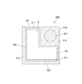
図1には、本実施形態に係る有機EL表示装置100が概略的に示されている。この図に示されるように、有機EL表示装置100は、上フレーム110及び下フレーム120に挟まれるように固定された有機ELパネル200から構成されている。
FIG. 1 schematically shows an organic
図2には、図1の有機ELパネル200の構成が示されている。有機ELパネル200は、TFT(Thin Film Transistor:薄膜トランジスタ)基板220と封止基板230との2枚の基板を有し、これらの基板の間には透明樹脂241(図4参照)が充填されている。TFT基板220は、表示領域202にマトリクス状に配置された画素を有している。ここで画素は、異なる色を発光する副画素280の組合せにより構成されている。また、TFT基板220には、副画素280のそれぞれに配置された画素トランジスタの走査信号線(不図示)に対してソース・ドレイン間を導通させるための電位を印加すると共に、各画素トランジスタのデータ信号線に対して画素の階調値に対応する電圧を印加する駆動回路である駆動IC(Integrated Circuit)260が載置されている。なお、TFTには、LTPS半導体、アモルファス半導体、酸化物半導体その他の半導体を用いることができる。
FIG. 2 shows the configuration of the
また、本実施形態に係る有機ELパネル200において、TFT基板220の表示領域202に配置された各副画素280の発光素子は白色を発光し、封止基板230においてR(赤)G(緑)B(青)W(白)の4色の光として透過させることにより、カラー表示を行うものとする。しかしながら、RGBの3色その他の色の組合せを用いてもよいし、TFT基板220における発光素子が白色の一色でなく、複数の色を発光することによりカラー表示を行うものであってもよい。この場合おいては、封止基板230にカラーフィルタを用いない構成とすることもできる。
In the
図3は、図2の表示領域202における9つの副画素280について、封止基板230のブラックマトリクス310の配置と、TFT基板220の発光領域E及びコンタクトホール291の配置とを比較して示す平面図である。ここで、ブラックマトリクス310は、カラーフィルタ等が配置された各副画素280の間において、隣接する副画素280からの光を透過させないようするための遮光膜であり、隣接する光の透過領域の間に形成されている。この図に示されるように、各画素は、Rのカラーフィルタが形成されたR領域232を有するR副画素、Gのカラーフィルタが形成されたG領域233を有するG副画素、Bのカラーフィルタが形成されたB領域234を有するB副画素、及びカラーフィルタを有さないW領域235を有するW副画素の4つの副画素280から構成され、4つの副画素280の組合せにより一つの画素のとして機能する。
FIG. 3 is a plan view showing the arrangement of the
この図の各副画素280には、TFT基板220において白色を発光する発光領域Eの配置、及び後述する下部電極224をトランジスタのソース又はドレインの電極228(図4参照)と接続させるためのコンタクトホール291の配置が示されている。このように本実施形態においては、発光領域Eはコンタクトホール291を避けてL字型に形成されている。またこのL字型に合わせるように各RGBW領域232〜235がそれぞれ形成されているが、これらは平面視において完全に一致していない。L字型の発光領域Eは、隣接する画素において発光された光の影響を受けやすい隣接画素に近い部分において、画素の辺に沿って長く形成される長辺322と、長辺322より短く形成された短辺321とを有している。本実施形態においては、ブラックマトリクス310は、発光領域Eの長辺322を覆うように形成され、発光領域Eの短辺321が露出するように形成されている。また、ブラックマトリクス310は、コンタクトホール291を覆うように形成されている。
In each of the
図4には、図3のA−A線における断面が示されている。この図に示されるように、TFT基板220は、ガラス基板等の透明な絶縁基板221と、トランジスタの制御に用いられる配線等を絶縁する層間絶縁膜222と、有機絶縁材料により形成された平坦化膜223と、トランジスタの一方の電極に電気的に接続され、平坦化膜223上に形成された下部電極224と、下部電極224の端部を覆い、隣接する副画素との間を絶縁する画素分離膜225と、下部電極224上及び画素分離膜225上で表示領域202全体を覆うように形成され、白色に発光する発光層を含む有機層と該有機層上に形成された透明電極からなる上部電極とからなる有機層・上部電極層226と、有機層・上部電極層226を覆うように形成された無機封止絶縁膜227と、を有している。
FIG. 4 shows a cross section taken along line AA of FIG. As shown in this figure, the
また、図4には、封止基板230の構成の一部として、ガラス基板等の透明な絶縁基板231と、各副画素の間から漏れる光を遮光するブラックマトリクス310のうち狭い幅で形成された幅狭部311及び広い幅で形成された幅広部312と、カラーフィルタであるG領域233及びB領域234とが示されている。TFT基板220と封止基板230とは透明樹脂241により接着されている。ここで、発光領域Eは、下部電極224と有機層・上部電極層226とが接している領域である。ブラックマトリクス310の幅広部312は、発光領域Eの周囲の画素分離膜225が形成する、有機層・上部電極層226が発光領域と比較して傾斜している有機層傾斜領域Pを覆っており、ブラックマトリクス310の幅狭部311は、この有機層傾斜領域Pを覆っていない。つまり、発光領域Eの長辺322に対応するブラックマトリクス310は、有機層傾斜領域Pを覆う幅広部312で形成され、発光領域Eの短辺321に対応するブラックマトリクス310は、有機層傾斜領域Pを覆わない幅狭部311で形成されている。
In FIG. 4, as a part of the structure of the sealing
図5には、図3のB−B線における断面が示されている。この断面は、R領域232を有する副画素及びB領域234を有する副画素を横切る断面であり、図4のA−A線における断面と異なり、コンタクトホール291を横切っている。この図に示されるように、ブラックマトリクス310は、コンタクトホール291を覆うように形成されたブラックマトリクス310のコンタクトホール遮光部313を有している。ここで、コンタクトホール遮光部313は、その端部において隣接画素から離れているため、有機層傾斜領域Pを覆わないように形成され、発光効率が高められている。
FIG. 5 shows a cross section taken along line BB in FIG. This cross section is a cross section that crosses the sub-pixel having the
図6は、一つの副画素280のブラックマトリクス310について示す平面図である。この図に示されるように、発光領域Eは、副画素280の形状の一辺に沿って延びる長さが長い長辺322と、副画素280の形状の他の一辺に沿って延びる長さが短い短辺321とを有している。また、長辺322に沿う副画素280の一辺に対応するブラックマトリクス310は、有機層傾斜領域Pを覆う幅広部312であり、短辺321に沿う副画素280の一辺に対応するブラックマトリクス310は、有機層傾斜領域Pを覆わない幅狭部311である。コンタクトホール遮光部313は、コンタクトホール291全体を覆うように形成されると共に、発光領域E側において有機層傾斜領域Pを覆わないように形成される。
FIG. 6 is a plan view showing the
以上説明したように、本実施形態によれば、幅広部312が、多くの乱反射が起こる発光領域の長辺322の有機層傾斜領域Pを遮光するため、光学的混色を抑えることができる。また、発光領域Eの短辺321の有機層傾斜領域Pは覆わないように形成される幅狭部311は、幅広部312が有機層傾斜領域Pを遮光している場合であっても、発光効率の低下を抑えることができる。また、コンタクトホール遮光部313は、コンタクトホール291全体を覆っているため、コンタクトホール291の斜面で発生する乱反射による光学的混色を抑えることができる。一方、コンタクトホール遮光部313は、発光領域Eに面する辺において、有機層傾斜領域Pを覆わないため、発光効率の低下を抑えている。したがって、本実施形態の有機EL表示装置によれば、発光効率の低下を抑えつつ、光学的混色を抑止することができる。
As described above, according to the present embodiment, the
図7には、上述の有機EL表示装置の変形例が、図4と同様の視野により示されている。図4に示される形態と異なる点は、幅広部312は、無機封止絶縁膜227の傾斜部分である封止膜傾斜領域Qを覆い、幅狭部311は封止膜傾斜領域Qを覆っていない点である。封止膜傾斜領域Qは発光領域Eの縁部分付近に形成される、発光領域Eの中央部分と比較して傾斜している領域である。乱反射は、有機層傾斜領域Pだけでなく、封止膜傾斜領域Qにおいても発生していることが考えられる。したがって、幅広部312は、有機層傾斜領域Pよりも発光領域E側に形成される封止膜傾斜領域Qを覆うようにすることにより、より光学的混色を抑えることができる。また、このように構成した場合であっても、上述の実施形態と同様の効果を得ることができる。
FIG. 7 shows a modified example of the above-described organic EL display device with the same field of view as FIG. 4 differs from the embodiment shown in FIG. 4 in that the
なお、上述の実施形態においては、発光領域EをL字型としたが、この形状に限られることなく、ブラックマトリクスが幅広部と幅狭部を有していればよい。また、更に、発光領域Eが画素の辺に沿った短辺と長辺を有している場合には、短辺に対応するブラックマトリクスが幅狭部であり、長辺に対応するブラックマトリクスが幅広部であることとすることができる。 In the above-described embodiment, the light emitting region E is L-shaped, but is not limited to this shape, and the black matrix may have a wide portion and a narrow portion. Further, when the light emitting region E has a short side and a long side along the side of the pixel, the black matrix corresponding to the short side is a narrow portion, and the black matrix corresponding to the long side is It can be a wide part.
100 有機EL表示装置、110 上フレーム、120 下フレーム、200 有機ELパネル、202 表示領域、220 TFT基板、221 絶縁基板、222 層間絶縁膜、223 平坦化膜、224 下部電極、225 画素分離膜、226 上部電極層、227 無機封止絶縁膜、228 電極、230 封止基板、231 絶縁基板、232 R領域、233 G領域、234 B領域、235 W領域、241 透明樹脂、280 副画素、291 コンタクトホール、310 ブラックマトリクス、311 幅狭部、312 幅広部、313 コンタクトホール遮光部、321 短辺、322 長辺。 100 organic EL display device, 110 upper frame, 120 lower frame, 200 organic EL panel, 202 display area, 220 TFT substrate, 221 insulating substrate, 222 interlayer insulating film, 223 planarizing film, 224 lower electrode, 225 pixel isolation film, 226 Upper electrode layer, 227 Inorganic sealing insulating film, 228 electrode, 230 sealing substrate, 231 insulating substrate, 232 R region, 233 G region, 234 B region, 235 W region, 241 transparent resin, 280 subpixel, 291 contact Hole, 310 black matrix, 311 narrow portion, 312 wide portion, 313 contact hole light shielding portion, 321 short side, 322 long side.
Claims (6)
前記複数の画素の境界を遮光する遮光膜と、
前記複数の画素のそれぞれにおいて、下部電極及び上部電極の間に配置され、発光する有機材料からなる発光層を含む複数の層からなる有機層が、前記下部電極と接触している領域である発光領域と、を備え、
前記発光領域は、前記複数の画素のそれぞれにおいて、前記画素の形状の辺に沿って延びると共に、互いに平行でない複数の長辺及び、前記複数の長辺よりも短く、互いに平行でない複数の短辺を有し、
前記遮光膜は、前記画素の辺に沿って配置され、互いに幅の異なる幅広部及び幅狭部を有し、
前記幅広部は、前記複数の長辺に対応する前記画素の辺に沿って配置され、前記幅狭部は、前記複数の短辺に対応する前記画素の辺に沿って配置され、
前記複数の長辺はそれぞれ、平面的に見て前記遮光膜と重畳し、前記複数の短辺はそれぞれ、平面的に見て前記遮光膜から露出している、ことを特徴とする有機EL表示装置。 A plurality of pixels arranged in a matrix on the substrate;
A light shielding film that shields a boundary between the plurality of pixels;
In each of the plurality of pixels, an organic layer composed of a plurality of layers including a light emitting layer made of an organic material that emits light and is disposed between the lower electrode and the upper electrode is a region that is in contact with the lower electrode. An area, and
The light emitting region in each of the plurality of pixels, extends along the sides of the shape of the pixels, a plurality of long sides and not parallel to each other, said shorter than a plurality of the long sides, a plurality of short sides are not parallel to each other Have
The light shielding film is disposed along the side of the pixel, and has a wide portion and a narrow portion having different widths,
The wide portion is disposed along a side of the pixel corresponding to the plurality of long sides, and the narrow portion is disposed along a side of the pixel corresponding to the plurality of short sides,
Each of the plurality of long sides, overlap the light shielding film in plan view, each of the plurality of short side is exposed from the light shielding film in plan view, it organic EL display, wherein apparatus.
前記複数の画素の一に含まれる前記発光領域と、前記複数の画素の一に隣接する他の一に含まれる前記発光領域とは、互いの短辺が対向するように隣接するか、あるいは互いの長辺が対向するように隣接し、
前記幅広部は、対向する前記互いの長辺間の距離よりも幅が大きく、
前記幅狭部は、対向する前記互いの短辺間の距離よりも幅が小さい、ことを特徴とする有機EL表示装置。 The organic EL display device according to claim 1,
The light emitting region included in one of the plurality of pixels and the light emitting region included in another adjacent to one of the plurality of pixels are adjacent to each other such that their short sides are opposed to each other, or to each other. Adjacent so that the long sides of
The wide part has a width larger than the distance between the opposing long sides,
The organic EL display device, wherein the narrow portion has a width smaller than a distance between the opposing short sides.
前記幅広部は、前記発光領域の周囲の前記有機層及び前記上部電極が前記発光領域と比較して傾斜して形成されている有機層傾斜領域を、平面視で覆う幅であり、
前記幅狭部は、前記有機層傾斜領域に達しない幅である、ことを特徴とする有機EL表示装置。 An organic EL display device according to claim 1 or 2,
The wide portion is a width that covers the organic layer inclined region in which the organic layer and the upper electrode around the light emitting region are formed to be inclined as compared with the light emitting region in a plan view,
The organic EL display device, wherein the narrow portion has a width that does not reach the organic layer inclined region.
前記幅広部は、前記上部電極上において前記複数の画素を覆うように形成された無機封止膜が、前記無機封止膜における前記発光領域の中央部分と比較して傾斜して形成されている封止膜傾斜領域を、上面からの視野において覆う幅である、ことを特徴とする有機EL表示装置。 An organic EL display device according to any one of claims 1 to 3,
The wide portion is formed by inclining an inorganic sealing film formed on the upper electrode so as to cover the plurality of pixels as compared with a central portion of the light emitting region in the inorganic sealing film. An organic EL display device having a width that covers a sealing film inclined region in a visual field from above.
前記遮光膜は、前記下部電極とトランジスタを接続するコンタクトホールを平面視において覆っている、ことを特徴とする有機EL表示装置。 An organic EL display device according to any one of claims 1 to 4,
The organic EL display device, wherein the light shielding film covers a contact hole connecting the lower electrode and the transistor in a plan view.
隣接する2つの前記発光領域は、前記幅広部あるいは前記幅狭部に対して線対称形状である、ことを特徴とする有機EL表示装置。 An organic EL display device according to any one of claims 2 to 5,
2. The organic EL display device, wherein two adjacent light emitting regions are line symmetrical with respect to the wide portion or the narrow portion.
Priority Applications (2)
| Application Number | Priority Date | Filing Date | Title |
|---|---|---|---|
| JP2013168995A JP6230328B2 (en) | 2013-08-15 | 2013-08-15 | Organic EL display device |
| US14/458,304 US9184416B2 (en) | 2013-08-15 | 2014-08-13 | Organic electro luminescent display device |
Applications Claiming Priority (1)
| Application Number | Priority Date | Filing Date | Title |
|---|---|---|---|
| JP2013168995A JP6230328B2 (en) | 2013-08-15 | 2013-08-15 | Organic EL display device |
Publications (3)
| Publication Number | Publication Date |
|---|---|
| JP2015037065A JP2015037065A (en) | 2015-02-23 |
| JP2015037065A5 JP2015037065A5 (en) | 2016-10-13 |
| JP6230328B2 true JP6230328B2 (en) | 2017-11-15 |
Family
ID=52466195
Family Applications (1)
| Application Number | Title | Priority Date | Filing Date |
|---|---|---|---|
| JP2013168995A Active JP6230328B2 (en) | 2013-08-15 | 2013-08-15 | Organic EL display device |
Country Status (2)
| Country | Link |
|---|---|
| US (1) | US9184416B2 (en) |
| JP (1) | JP6230328B2 (en) |
Families Citing this family (7)
| Publication number | Priority date | Publication date | Assignee | Title |
|---|---|---|---|---|
| KR102239842B1 (en) * | 2014-07-30 | 2021-04-14 | 삼성디스플레이 주식회사 | Organic light emitting display apparatus |
| JP6685675B2 (en) * | 2015-09-07 | 2020-04-22 | 株式会社Joled | Organic EL device, organic EL display panel using the same, and method for manufacturing organic EL display panel |
| JP2017062941A (en) * | 2015-09-25 | 2017-03-30 | ソニー株式会社 | Display device and manufacturing method for the same |
| KR102515963B1 (en) * | 2016-03-04 | 2023-03-30 | 삼성디스플레이 주식회사 | Organic light emitting display panel |
| CN110021651B (en) * | 2019-03-29 | 2021-02-23 | 武汉华星光电技术有限公司 | Display panel and electronic device |
| KR20210149271A (en) * | 2020-06-01 | 2021-12-09 | 삼성디스플레이 주식회사 | Display device |
| KR20220135273A (en) * | 2021-03-29 | 2022-10-07 | 삼성디스플레이 주식회사 | Display panel and vehicle including display panel |
Family Cites Families (9)
| Publication number | Priority date | Publication date | Assignee | Title |
|---|---|---|---|---|
| US7821065B2 (en) * | 1999-03-02 | 2010-10-26 | Semiconductor Energy Laboratory Co., Ltd. | Semiconductor device comprising a thin film transistor comprising a semiconductor thin film and method of manufacturing the same |
| TW466888B (en) | 2000-09-29 | 2001-12-01 | Ind Tech Res Inst | Pixel device structure and process of organic light emitting diode display |
| US6744198B2 (en) * | 2001-03-19 | 2004-06-01 | Seiko Epson Corporation | Method for manufacturing display device, display device, and electronic apparatus |
| US7098069B2 (en) * | 2002-01-24 | 2006-08-29 | Semiconductor Energy Laboratory Co., Ltd. | Light emitting device, method of preparing the same and device for fabricating the same |
| JP2007188653A (en) * | 2006-01-11 | 2007-07-26 | Seiko Epson Corp | Light emitting unit and electronic apparatus |
| JP2008096966A (en) * | 2006-09-12 | 2008-04-24 | Seiko Epson Corp | Electro-optical device and electronic equipment |
| JP4858054B2 (en) | 2006-09-29 | 2012-01-18 | セイコーエプソン株式会社 | LIGHT EMITTING DEVICE AND ELECTRONIC DEVICE |
| JP4893392B2 (en) * | 2007-03-15 | 2012-03-07 | ソニー株式会社 | Display device and electronic device |
| US8735874B2 (en) * | 2011-02-14 | 2014-05-27 | Semiconductor Energy Laboratory Co., Ltd. | Light-emitting device, display device, and method for manufacturing the same |
-
2013
- 2013-08-15 JP JP2013168995A patent/JP6230328B2/en active Active
-
2014
- 2014-08-13 US US14/458,304 patent/US9184416B2/en active Active
Also Published As
| Publication number | Publication date |
|---|---|
| US9184416B2 (en) | 2015-11-10 |
| JP2015037065A (en) | 2015-02-23 |
| US20150048347A1 (en) | 2015-02-19 |
Similar Documents
| Publication | Publication Date | Title |
|---|---|---|
| JP6230328B2 (en) | Organic EL display device | |
| JP6170421B2 (en) | Organic EL display device | |
| JP6104099B2 (en) | Organic EL display device | |
| JP6560530B2 (en) | Display device | |
| KR102576557B1 (en) | Organic light emitting display device | |
| US10062870B2 (en) | Display device including a diffraction grating | |
| US9087797B2 (en) | Light-emitting element display device | |
| KR20160058360A (en) | Narrow Bezel Large Area Organic Light Emitting Diode Display | |
| US9660002B2 (en) | Display device | |
| KR102458911B1 (en) | Both Side Emission Type Transparent Organic Light Emitting Diode Display | |
| JP6247855B2 (en) | Light emitting element display device | |
| KR101584894B1 (en) | Display device | |
| JP6749160B2 (en) | Display device | |
| JP6258047B2 (en) | Light emitting element display device | |
| WO2018229859A1 (en) | Display device, method for producing display device, and apparatus for producing display device | |
| US20150090987A1 (en) | Organic el display device | |
| JP6325318B2 (en) | Display device | |
| JP6492403B2 (en) | Organic EL device, method for manufacturing organic EL device, electronic device | |
| JP2015069757A (en) | Organic el display device | |
| JP2016045307A (en) | Display device | |
| KR102387550B1 (en) | Display device | |
| KR102484901B1 (en) | Organic Light Emitting Diode Display Device | |
| JP2015008095A (en) | Organic el display device |
Legal Events
| Date | Code | Title | Description |
|---|---|---|---|
| A521 | Request for written amendment filed |
Free format text: JAPANESE INTERMEDIATE CODE: A523 Effective date: 20160808 |
|
| A621 | Written request for application examination |
Free format text: JAPANESE INTERMEDIATE CODE: A621 Effective date: 20160808 |
|
| A977 | Report on retrieval |
Free format text: JAPANESE INTERMEDIATE CODE: A971007 Effective date: 20170316 |
|
| A131 | Notification of reasons for refusal |
Free format text: JAPANESE INTERMEDIATE CODE: A131 Effective date: 20170328 |
|
| A521 | Request for written amendment filed |
Free format text: JAPANESE INTERMEDIATE CODE: A523 Effective date: 20170522 |
|
| TRDD | Decision of grant or rejection written | ||
| A01 | Written decision to grant a patent or to grant a registration (utility model) |
Free format text: JAPANESE INTERMEDIATE CODE: A01 Effective date: 20171003 |
|
| A61 | First payment of annual fees (during grant procedure) |
Free format text: JAPANESE INTERMEDIATE CODE: A61 Effective date: 20171017 |
|
| R150 | Certificate of patent or registration of utility model |
Ref document number: 6230328 Country of ref document: JP Free format text: JAPANESE INTERMEDIATE CODE: R150 |
|
| R250 | Receipt of annual fees |
Free format text: JAPANESE INTERMEDIATE CODE: R250 |
|
| R250 | Receipt of annual fees |
Free format text: JAPANESE INTERMEDIATE CODE: R250 |
|
| R250 | Receipt of annual fees |
Free format text: JAPANESE INTERMEDIATE CODE: R250 |
|
| R250 | Receipt of annual fees |
Free format text: JAPANESE INTERMEDIATE CODE: R250 |