JP6217841B2 - モジュールおよびこのモジュールの製造方法 - Google Patents
モジュールおよびこのモジュールの製造方法 Download PDFInfo
- Publication number
- JP6217841B2 JP6217841B2 JP2016508639A JP2016508639A JP6217841B2 JP 6217841 B2 JP6217841 B2 JP 6217841B2 JP 2016508639 A JP2016508639 A JP 2016508639A JP 2016508639 A JP2016508639 A JP 2016508639A JP 6217841 B2 JP6217841 B2 JP 6217841B2
- Authority
- JP
- Japan
- Prior art keywords
- metal pins
- metal
- insulating layer
- coil
- pins
- Prior art date
- Legal status (The legal status is an assumption and is not a legal conclusion. Google has not performed a legal analysis and makes no representation as to the accuracy of the status listed.)
- Expired - Fee Related
Links
- 238000004519 manufacturing process Methods 0.000 title claims description 14
- 238000000034 method Methods 0.000 title claims description 10
- 229910052751 metal Inorganic materials 0.000 claims description 228
- 239000002184 metal Substances 0.000 claims description 228
- 238000005530 etching Methods 0.000 claims description 11
- 230000002093 peripheral effect Effects 0.000 claims description 6
- 150000002739 metals Chemical class 0.000 claims description 3
- 238000000227 grinding Methods 0.000 claims description 2
- 238000005498 polishing Methods 0.000 claims description 2
- 230000017525 heat dissipation Effects 0.000 description 24
- 229920005989 resin Polymers 0.000 description 21
- 239000011347 resin Substances 0.000 description 21
- 239000004020 conductor Substances 0.000 description 12
- 238000000576 coating method Methods 0.000 description 9
- 239000011248 coating agent Substances 0.000 description 7
- 239000000758 substrate Substances 0.000 description 6
- 229910052802 copper Inorganic materials 0.000 description 5
- 229910052709 silver Inorganic materials 0.000 description 4
- 230000035882 stress Effects 0.000 description 4
- 229920001187 thermosetting polymer Polymers 0.000 description 4
- 239000003822 epoxy resin Substances 0.000 description 3
- 239000010931 gold Substances 0.000 description 3
- 239000012212 insulator Substances 0.000 description 3
- 239000000463 material Substances 0.000 description 3
- 229920000647 polyepoxide Polymers 0.000 description 3
- 229910052581 Si3N4 Inorganic materials 0.000 description 2
- 229910045601 alloy Inorganic materials 0.000 description 2
- 239000000956 alloy Substances 0.000 description 2
- 229910052782 aluminium Inorganic materials 0.000 description 2
- 238000005452 bending Methods 0.000 description 2
- 239000000919 ceramic Substances 0.000 description 2
- PMHQVHHXPFUNSP-UHFFFAOYSA-M copper(1+);methylsulfanylmethane;bromide Chemical compound Br[Cu].CSC PMHQVHHXPFUNSP-UHFFFAOYSA-M 0.000 description 2
- 230000006355 external stress Effects 0.000 description 2
- 229910052737 gold Inorganic materials 0.000 description 2
- 238000009413 insulation Methods 0.000 description 2
- JEIPFZHSYJVQDO-UHFFFAOYSA-N iron(III) oxide Inorganic materials O=[Fe]O[Fe]=O JEIPFZHSYJVQDO-UHFFFAOYSA-N 0.000 description 2
- 239000007769 metal material Substances 0.000 description 2
- 230000002265 prevention Effects 0.000 description 2
- 230000005855 radiation Effects 0.000 description 2
- 238000007650 screen-printing Methods 0.000 description 2
- HQVNEWCFYHHQES-UHFFFAOYSA-N silicon nitride Chemical compound N12[Si]34N5[Si]62N3[Si]51N64 HQVNEWCFYHHQES-UHFFFAOYSA-N 0.000 description 2
- 229910002482 Cu–Ni Inorganic materials 0.000 description 1
- 229910017827 Cu—Fe Inorganic materials 0.000 description 1
- 230000006835 compression Effects 0.000 description 1
- 238000007906 compression Methods 0.000 description 1
- 230000007797 corrosion Effects 0.000 description 1
- 238000005260 corrosion Methods 0.000 description 1
- 230000006866 deterioration Effects 0.000 description 1
- 230000002542 deteriorative effect Effects 0.000 description 1
- 238000010586 diagram Methods 0.000 description 1
- 230000004907 flux Effects 0.000 description 1
- PCHJSUWPFVWCPO-UHFFFAOYSA-N gold Chemical compound [Au] PCHJSUWPFVWCPO-UHFFFAOYSA-N 0.000 description 1
- 238000010030 laminating Methods 0.000 description 1
- 239000000696 magnetic material Substances 0.000 description 1
- 238000012986 modification Methods 0.000 description 1
- 230000004048 modification Effects 0.000 description 1
- 238000007747 plating Methods 0.000 description 1
- 238000007639 printing Methods 0.000 description 1
- 238000007789 sealing Methods 0.000 description 1
- 238000010008 shearing Methods 0.000 description 1
- 238000004804 winding Methods 0.000 description 1
- 229910000859 α-Fe Inorganic materials 0.000 description 1
Images

Classifications
-
- H—ELECTRICITY
- H01—ELECTRIC ELEMENTS
- H01F—MAGNETS; INDUCTANCES; TRANSFORMERS; SELECTION OF MATERIALS FOR THEIR MAGNETIC PROPERTIES
- H01F27/00—Details of transformers or inductances, in general
- H01F27/24—Magnetic cores
-
- H—ELECTRICITY
- H01—ELECTRIC ELEMENTS
- H01F—MAGNETS; INDUCTANCES; TRANSFORMERS; SELECTION OF MATERIALS FOR THEIR MAGNETIC PROPERTIES
- H01F17/00—Fixed inductances of the signal type
- H01F17/0006—Printed inductances
- H01F17/0013—Printed inductances with stacked layers
-
- H—ELECTRICITY
- H01—ELECTRIC ELEMENTS
- H01F—MAGNETS; INDUCTANCES; TRANSFORMERS; SELECTION OF MATERIALS FOR THEIR MAGNETIC PROPERTIES
- H01F17/00—Fixed inductances of the signal type
- H01F17/04—Fixed inductances of the signal type with magnetic core
- H01F17/06—Fixed inductances of the signal type with magnetic core with core substantially closed in itself, e.g. toroid
-
- H—ELECTRICITY
- H01—ELECTRIC ELEMENTS
- H01F—MAGNETS; INDUCTANCES; TRANSFORMERS; SELECTION OF MATERIALS FOR THEIR MAGNETIC PROPERTIES
- H01F27/00—Details of transformers or inductances, in general
- H01F27/08—Cooling; Ventilating
- H01F27/22—Cooling by heat conduction through solid or powdered fillings
-
- H—ELECTRICITY
- H01—ELECTRIC ELEMENTS
- H01F—MAGNETS; INDUCTANCES; TRANSFORMERS; SELECTION OF MATERIALS FOR THEIR MAGNETIC PROPERTIES
- H01F27/00—Details of transformers or inductances, in general
- H01F27/28—Coils; Windings; Conductive connections
- H01F27/2804—Printed windings
-
- H—ELECTRICITY
- H01—ELECTRIC ELEMENTS
- H01F—MAGNETS; INDUCTANCES; TRANSFORMERS; SELECTION OF MATERIALS FOR THEIR MAGNETIC PROPERTIES
- H01F27/00—Details of transformers or inductances, in general
- H01F27/28—Coils; Windings; Conductive connections
- H01F27/2876—Cooling
-
- H—ELECTRICITY
- H01—ELECTRIC ELEMENTS
- H01F—MAGNETS; INDUCTANCES; TRANSFORMERS; SELECTION OF MATERIALS FOR THEIR MAGNETIC PROPERTIES
- H01F41/00—Apparatus or processes specially adapted for manufacturing or assembling magnets, inductances or transformers; Apparatus or processes specially adapted for manufacturing materials characterised by their magnetic properties
- H01F41/02—Apparatus or processes specially adapted for manufacturing or assembling magnets, inductances or transformers; Apparatus or processes specially adapted for manufacturing materials characterised by their magnetic properties for manufacturing cores, coils, or magnets
- H01F41/04—Apparatus or processes specially adapted for manufacturing or assembling magnets, inductances or transformers; Apparatus or processes specially adapted for manufacturing materials characterised by their magnetic properties for manufacturing cores, coils, or magnets for manufacturing coils
- H01F41/041—Printed circuit coils
- H01F41/046—Printed circuit coils structurally combined with ferromagnetic material
Landscapes
- Engineering & Computer Science (AREA)
- Power Engineering (AREA)
- Microelectronics & Electronic Packaging (AREA)
- Manufacturing & Machinery (AREA)
- Coils Or Transformers For Communication (AREA)
- Manufacturing Cores, Coils, And Magnets (AREA)
Description
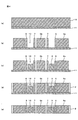
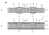
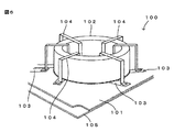
次に、モジュール1の製造方法について、図4および図5を参照して、各金属ピン6,7および放熱用の金属体5a,5bを、それぞれ同じ金属であるCuで形成する場合を例として説明する。なお、図4および図5それぞれは、モジュール1の製造方法を説明するための図であり、図4(a)〜(e)はその各工程、図5(a)および(b)は、図4(e)に続く各工程を示す。
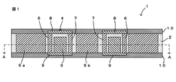
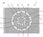
2 絶縁層
3 磁性体コア(コイルコア)
4 コイル電極
5a,5b 金属体(放熱用部材)
6 外側金属ピン
7 内側金属ピン
8 上側配線電極(第1接続部材)
9 下側配線電極(第2接続部材)
Claims (5)
- 絶縁層と、
前記絶縁層に内蔵された環状のコイルコアと、
前記コイルコアを巻回するように前記絶縁層に設けられたコイル電極と、
前記コイルコアの外側の前記絶縁層内に配置された放熱用部材とを備え、
前記コイル電極は、
前記コイルコアの周方向に交差するように配置され、前記コイルコアの外周面に沿って配列された複数の外側金属ピンと、前記コイルコアの周方向に交差するように配置され、前記各外側金属ピンそれぞれと複数の対を成すように前記コイルコアの内周面に沿って配列された複数の内側金属ピンと、各対を成す前記外側金属ピンおよび前記内側金属ピンの一方の端面同士を接続する複数の第1接続部材と、前記外側金属ピンの他方の端面と、対を成す前記内側金属ピンの所定側に隣接する前記内側金属ピンの他方の端面とをそれぞれ接続する複数の第2接続部材とを有し、
前記放熱用部材と前記複数の外側金属ピンと前記複数の内側金属ピンとは、前記コイルコアの周方向に直交する方向の高さが等しいことを特徴とするモジュール。 - 前記コイルコアの内側の前記絶縁層内に、前記放熱用部材がさらに配置されていることを特徴とする請求項1に記載のモジュール。
- 前記各外側金属ピン、前記各内側金属ピンおよび前記放熱用部材が、同一の金属で形成されていることを特徴とする請求項1または2に記載のモジュール。
- 前記各外側金属ピンおよび前記各内側金属ピンと、前記放熱用部材とが異なる金属で形成されていることを特徴とする請求項1または2に記載のモジュール。
- 平板状の支持体の一方主面に貼り付けられた金属板を準備する工程と、
前記金属板をエッチングすることにより、前記支持体の一方主面に立設されて環状に配列される複数の外側金属ピンと、前記各外側金属ピンの内側でコイルコアの配置スペースを挟み、前記支持体の一方主面に立設されて環状に配列され前記各外側金属ピンそれぞれと複数の対を成す複数の内側金属ピンと、前記各外側金属ピンの外側および前記各内側金属ピンの内側のうち、少なくとも前記各外側金属ピンの外側に配置される放熱用部材としての金属体とを同時形成する工程と、
前記配置スペースに前記コイルコアを配置する工程と、
前記支持体の一方主面、前記コイルコア、前記各外側金属ピン、前記各内側金属ピンおよび前記金属体を封止する絶縁層を形成する工程と、
研磨または研削により、前記支持体を除去するとともに、前記各外側金属ピンおよび前記各内側金属ピンそれぞれの両端面を前記絶縁層から露出させる工程と、
各対を成す前記外側金属ピンおよび前記内側金属ピンの一方の端面同士を接続する複数の第1接続部材と、前記外側金属ピンの他方の端面と、対を成す前記内側金属ピンの所定側に隣接する前記内側金属ピンの他方の端面とをそれぞれ接続する複数の第2接続部材とを形成する工程とを備えることを特徴とするモジュールの製造方法。
Applications Claiming Priority (3)
| Application Number | Priority Date | Filing Date | Title |
|---|---|---|---|
| JP2014054855 | 2014-03-18 | ||
| JP2014054855 | 2014-03-18 | ||
| PCT/JP2015/055642 WO2015141434A1 (ja) | 2014-03-18 | 2015-02-26 | モジュールおよびこのモジュールの製造方法 |
Publications (2)
| Publication Number | Publication Date |
|---|---|
| JPWO2015141434A1 JPWO2015141434A1 (ja) | 2017-04-06 |
| JP6217841B2 true JP6217841B2 (ja) | 2017-10-25 |
Family
ID=54144410
Family Applications (1)
| Application Number | Title | Priority Date | Filing Date |
|---|---|---|---|
| JP2016508639A Expired - Fee Related JP6217841B2 (ja) | 2014-03-18 | 2015-02-26 | モジュールおよびこのモジュールの製造方法 |
Country Status (3)
| Country | Link |
|---|---|
| US (1) | US10424430B2 (ja) |
| JP (1) | JP6217841B2 (ja) |
| WO (1) | WO2015141434A1 (ja) |
Families Citing this family (8)
| Publication number | Priority date | Publication date | Assignee | Title |
|---|---|---|---|---|
| WO2016043306A1 (ja) * | 2014-09-19 | 2016-03-24 | 株式会社村田製作所 | インダクタ部品およびインダクタ部品の製造方法 |
| US9824811B2 (en) * | 2014-12-19 | 2017-11-21 | Texas Instruments Incorporated | Embedded coil assembly and method of making |
| WO2017119423A1 (ja) * | 2016-01-06 | 2017-07-13 | 株式会社村田製作所 | インダクタ部品およびインダクタ部品の製造方法 |
| JP7176544B2 (ja) * | 2020-02-19 | 2022-11-22 | 株式会社村田製作所 | インダクタ部品およびその製造方法 |
| JP7173066B2 (ja) * | 2020-02-19 | 2022-11-16 | 株式会社村田製作所 | インダクタ部品およびその製造方法 |
| JP7247941B2 (ja) * | 2020-04-08 | 2023-03-29 | 株式会社村田製作所 | インダクタ部品およびその製造方法 |
| GB202117336D0 (en) * | 2021-12-01 | 2022-01-12 | Rolls Royce Plc | Inductor |
| CN114898965A (zh) * | 2022-04-15 | 2022-08-12 | 广州致远电子有限公司 | 磁性线圈组件和磁性线圈组件制作方法 |
Family Cites Families (7)
| Publication number | Priority date | Publication date | Assignee | Title |
|---|---|---|---|---|
| JP4485740B2 (ja) * | 2002-12-06 | 2010-06-23 | 東光株式会社 | 積層型電子部品 |
| US7158005B2 (en) * | 2005-02-10 | 2007-01-02 | Harris Corporation | Embedded toroidal inductor |
| JP2006278841A (ja) | 2005-03-30 | 2006-10-12 | Matsushita Electric Ind Co Ltd | コイル部品 |
| JP5046720B2 (ja) * | 2006-12-22 | 2012-10-10 | 京セラ株式会社 | コイル内蔵基板 |
| JP5270576B2 (ja) * | 2007-01-11 | 2013-08-21 | プラナーマグ インコーポレイテッド | 平面型広帯域トランス |
| JP2011243870A (ja) * | 2010-05-20 | 2011-12-01 | Denso Corp | コイル実装基板 |
| JP5556692B2 (ja) * | 2011-02-15 | 2014-07-23 | トヨタ自動車株式会社 | リアクトル |
-
2015
- 2015-02-26 WO PCT/JP2015/055642 patent/WO2015141434A1/ja not_active Ceased
- 2015-02-26 JP JP2016508639A patent/JP6217841B2/ja not_active Expired - Fee Related
-
2016
- 2016-09-16 US US15/267,729 patent/US10424430B2/en active Active
Also Published As
| Publication number | Publication date |
|---|---|
| US10424430B2 (en) | 2019-09-24 |
| WO2015141434A1 (ja) | 2015-09-24 |
| US20170004914A1 (en) | 2017-01-05 |
| JPWO2015141434A1 (ja) | 2017-04-06 |
Similar Documents
| Publication | Publication Date | Title |
|---|---|---|
| JP6217841B2 (ja) | モジュールおよびこのモジュールの製造方法 | |
| JP6837432B2 (ja) | 高周波モジュール | |
| JP6323553B2 (ja) | コイル部品 | |
| US10553347B2 (en) | Module | |
| JP6365692B2 (ja) | コイル部品 | |
| JP6292300B2 (ja) | コイル部品およびこのコイル部品を備えるモジュール | |
| JP6716866B2 (ja) | コイル部品 | |
| JP2009218531A (ja) | インダクタとその製造方法とこれを用いた回路モジュール | |
| US10418168B2 (en) | Inductor and method for manufacturing the same | |
| CN107112111B (zh) | 线圈部件 | |
| JP6716867B2 (ja) | コイル部品およびその製造方法 | |
| JP2010027996A (ja) | 高周波モジュール及びその製造方法 | |
| JP5045508B2 (ja) | インダクタとその製造方法とこれを用いた回路モジュール | |
| JP2023103038A (ja) | コイル装置 | |
| JPWO2016056426A1 (ja) | インダクタ部品 | |
| JP6315108B2 (ja) | パワー半導体のパッケージ素子 | |
| JP6520480B2 (ja) | コイル部品 | |
| JP6607312B2 (ja) | インダクタ部品 | |
| JP6432674B2 (ja) | インダクタ部品 | |
| JP2023088119A (ja) | インダクタ部品およびインダクタ部品の製造方法 | |
| JP2016131190A (ja) | コイル部品 | |
| WO2017188076A1 (ja) | インダクタ部品 |
Legal Events
| Date | Code | Title | Description |
|---|---|---|---|
| A131 | Notification of reasons for refusal |
Free format text: JAPANESE INTERMEDIATE CODE: A131 Effective date: 20170620 |
|
| A521 | Request for written amendment filed |
Free format text: JAPANESE INTERMEDIATE CODE: A523 Effective date: 20170818 |
|
| TRDD | Decision of grant or rejection written | ||
| A01 | Written decision to grant a patent or to grant a registration (utility model) |
Free format text: JAPANESE INTERMEDIATE CODE: A01 Effective date: 20170829 |
|
| A61 | First payment of annual fees (during grant procedure) |
Free format text: JAPANESE INTERMEDIATE CODE: A61 Effective date: 20170911 |
|
| R150 | Certificate of patent or registration of utility model |
Ref document number: 6217841 Country of ref document: JP Free format text: JAPANESE INTERMEDIATE CODE: R150 |
|
| LAPS | Cancellation because of no payment of annual fees |