JP6194869B2 - 半導体装置およびその製造方法 - Google Patents
半導体装置およびその製造方法 Download PDFInfo
- Publication number
- JP6194869B2 JP6194869B2 JP2014196498A JP2014196498A JP6194869B2 JP 6194869 B2 JP6194869 B2 JP 6194869B2 JP 2014196498 A JP2014196498 A JP 2014196498A JP 2014196498 A JP2014196498 A JP 2014196498A JP 6194869 B2 JP6194869 B2 JP 6194869B2
- Authority
- JP
- Japan
- Prior art keywords
- electrode
- semiconductor device
- layer
- insulating film
- semiconductor
- Prior art date
- Legal status (The legal status is an assumption and is not a legal conclusion. Google has not performed a legal analysis and makes no representation as to the accuracy of the status listed.)
- Active
Links
- 239000004065 semiconductor Substances 0.000 title claims description 385
- 238000004519 manufacturing process Methods 0.000 title claims description 70
- 238000000034 method Methods 0.000 claims description 104
- 238000001312 dry etching Methods 0.000 claims description 24
- JMASRVWKEDWRBT-UHFFFAOYSA-N Gallium nitride Chemical compound [Ga]#N JMASRVWKEDWRBT-UHFFFAOYSA-N 0.000 claims description 19
- 239000010410 layer Substances 0.000 description 307
- 230000008569 process Effects 0.000 description 80
- 230000001681 protective effect Effects 0.000 description 45
- 239000000758 substrate Substances 0.000 description 21
- VYPSYNLAJGMNEJ-UHFFFAOYSA-N Silicium dioxide Chemical compound O=[Si]=O VYPSYNLAJGMNEJ-UHFFFAOYSA-N 0.000 description 18
- 238000000231 atomic layer deposition Methods 0.000 description 15
- 239000010936 titanium Substances 0.000 description 12
- XUIMIQQOPSSXEZ-UHFFFAOYSA-N Silicon Chemical compound [Si] XUIMIQQOPSSXEZ-UHFFFAOYSA-N 0.000 description 10
- 229910052782 aluminium Inorganic materials 0.000 description 10
- XAGFODPZIPBFFR-UHFFFAOYSA-N aluminium Chemical compound [Al] XAGFODPZIPBFFR-UHFFFAOYSA-N 0.000 description 10
- 229910052710 silicon Inorganic materials 0.000 description 10
- 239000010703 silicon Substances 0.000 description 10
- KDLHZDBZIXYQEI-UHFFFAOYSA-N Palladium Chemical compound [Pd] KDLHZDBZIXYQEI-UHFFFAOYSA-N 0.000 description 9
- 229910004298 SiO 2 Inorganic materials 0.000 description 9
- 239000000463 material Substances 0.000 description 9
- 235000012239 silicon dioxide Nutrition 0.000 description 9
- 239000000377 silicon dioxide Substances 0.000 description 9
- 229910002601 GaN Inorganic materials 0.000 description 8
- RTAQQCXQSZGOHL-UHFFFAOYSA-N Titanium Chemical compound [Ti] RTAQQCXQSZGOHL-UHFFFAOYSA-N 0.000 description 6
- 238000000137 annealing Methods 0.000 description 6
- 238000010438 heat treatment Methods 0.000 description 6
- 239000011777 magnesium Substances 0.000 description 6
- 238000004544 sputter deposition Methods 0.000 description 6
- 229910052719 titanium Inorganic materials 0.000 description 6
- QCWXUUIWCKQGHC-UHFFFAOYSA-N Zirconium Chemical compound [Zr] QCWXUUIWCKQGHC-UHFFFAOYSA-N 0.000 description 5
- 230000000694 effects Effects 0.000 description 5
- 238000010030 laminating Methods 0.000 description 5
- 238000001039 wet etching Methods 0.000 description 5
- 229910052726 zirconium Inorganic materials 0.000 description 5
- 238000011109 contamination Methods 0.000 description 4
- 230000006866 deterioration Effects 0.000 description 4
- 238000010586 diagram Methods 0.000 description 4
- 230000005669 field effect Effects 0.000 description 4
- 238000009413 insulation Methods 0.000 description 4
- FYYHWMGAXLPEAU-UHFFFAOYSA-N Magnesium Chemical compound [Mg] FYYHWMGAXLPEAU-UHFFFAOYSA-N 0.000 description 3
- 238000010292 electrical insulation Methods 0.000 description 3
- 229910052749 magnesium Inorganic materials 0.000 description 3
- 229910052763 palladium Inorganic materials 0.000 description 3
- 239000011241 protective layer Substances 0.000 description 3
- PIGFYZPCRLYGLF-UHFFFAOYSA-N Aluminum nitride Chemical compound [Al]#N PIGFYZPCRLYGLF-UHFFFAOYSA-N 0.000 description 2
- RNQKDQAVIXDKAG-UHFFFAOYSA-N aluminum gallium Chemical compound [Al].[Ga] RNQKDQAVIXDKAG-UHFFFAOYSA-N 0.000 description 2
- AJGDITRVXRPLBY-UHFFFAOYSA-N aluminum indium Chemical compound [Al].[In] AJGDITRVXRPLBY-UHFFFAOYSA-N 0.000 description 2
- 230000004888 barrier function Effects 0.000 description 2
- 239000007789 gas Substances 0.000 description 2
- 238000012986 modification Methods 0.000 description 2
- 230000004048 modification Effects 0.000 description 2
- TWNQGVIAIRXVLR-UHFFFAOYSA-N oxo(oxoalumanyloxy)alumane Chemical compound O=[Al]O[Al]=O TWNQGVIAIRXVLR-UHFFFAOYSA-N 0.000 description 2
- HBMJWWWQQXIZIP-UHFFFAOYSA-N silicon carbide Chemical compound [Si+]#[C-] HBMJWWWQQXIZIP-UHFFFAOYSA-N 0.000 description 2
- 239000002356 single layer Substances 0.000 description 2
- 229910018072 Al 2 O 3 Inorganic materials 0.000 description 1
- JBRZTFJDHDCESZ-UHFFFAOYSA-N AsGa Chemical compound [As]#[Ga] JBRZTFJDHDCESZ-UHFFFAOYSA-N 0.000 description 1
- OKTJSMMVPCPJKN-UHFFFAOYSA-N Carbon Chemical compound [C] OKTJSMMVPCPJKN-UHFFFAOYSA-N 0.000 description 1
- 229910052581 Si3N4 Inorganic materials 0.000 description 1
- 229910004205 SiNX Inorganic materials 0.000 description 1
- QVGXLLKOCUKJST-UHFFFAOYSA-N atomic oxygen Chemical compound [O] QVGXLLKOCUKJST-UHFFFAOYSA-N 0.000 description 1
- 230000008901 benefit Effects 0.000 description 1
- 229910052799 carbon Inorganic materials 0.000 description 1
- 239000000969 carrier Substances 0.000 description 1
- 238000005229 chemical vapour deposition Methods 0.000 description 1
- PMHQVHHXPFUNSP-UHFFFAOYSA-M copper(1+);methylsulfanylmethane;bromide Chemical compound Br[Cu].CSC PMHQVHHXPFUNSP-UHFFFAOYSA-M 0.000 description 1
- 238000000151 deposition Methods 0.000 description 1
- 238000009792 diffusion process Methods 0.000 description 1
- 239000007772 electrode material Substances 0.000 description 1
- 238000005530 etching Methods 0.000 description 1
- 229910052732 germanium Inorganic materials 0.000 description 1
- GNPVGFCGXDBREM-UHFFFAOYSA-N germanium atom Chemical compound [Ge] GNPVGFCGXDBREM-UHFFFAOYSA-N 0.000 description 1
- 229910052735 hafnium Inorganic materials 0.000 description 1
- VBJZVLUMGGDVMO-UHFFFAOYSA-N hafnium atom Chemical compound [Hf] VBJZVLUMGGDVMO-UHFFFAOYSA-N 0.000 description 1
- CJNBYAVZURUTKZ-UHFFFAOYSA-N hafnium(iv) oxide Chemical compound O=[Hf]=O CJNBYAVZURUTKZ-UHFFFAOYSA-N 0.000 description 1
- 239000012528 membrane Substances 0.000 description 1
- 229910052751 metal Inorganic materials 0.000 description 1
- 239000002184 metal Substances 0.000 description 1
- 150000004767 nitrides Chemical class 0.000 description 1
- 229910052760 oxygen Inorganic materials 0.000 description 1
- 239000001301 oxygen Substances 0.000 description 1
- RVTZCBVAJQQJTK-UHFFFAOYSA-N oxygen(2-);zirconium(4+) Chemical compound [O-2].[O-2].[Zr+4] RVTZCBVAJQQJTK-UHFFFAOYSA-N 0.000 description 1
- 230000002093 peripheral effect Effects 0.000 description 1
- 229920002120 photoresistant polymer Polymers 0.000 description 1
- 238000005268 plasma chemical vapour deposition Methods 0.000 description 1
- 230000010287 polarization Effects 0.000 description 1
- HQVNEWCFYHHQES-UHFFFAOYSA-N silicon nitride Chemical compound N12[Si]34N5[Si]62N3[Si]51N64 HQVNEWCFYHHQES-UHFFFAOYSA-N 0.000 description 1
- 238000009751 slip forming Methods 0.000 description 1
- JBQYATWDVHIOAR-UHFFFAOYSA-N tellanylidenegermanium Chemical compound [Te]=[Ge] JBQYATWDVHIOAR-UHFFFAOYSA-N 0.000 description 1
- 230000005533 two-dimensional electron gas Effects 0.000 description 1
- 238000007740 vapor deposition Methods 0.000 description 1
- 229910001928 zirconium oxide Inorganic materials 0.000 description 1
Images


Classifications
-
- H—ELECTRICITY
- H01—ELECTRIC ELEMENTS
- H01L—SEMICONDUCTOR DEVICES NOT COVERED BY CLASS H10
- H01L29/00—Semiconductor devices adapted for rectifying, amplifying, oscillating or switching, or capacitors or resistors with at least one potential-jump barrier or surface barrier, e.g. PN junction depletion layer or carrier concentration layer; Details of semiconductor bodies or of electrodes thereof ; Multistep manufacturing processes therefor
- H01L29/02—Semiconductor bodies ; Multistep manufacturing processes therefor
- H01L29/12—Semiconductor bodies ; Multistep manufacturing processes therefor characterised by the materials of which they are formed
- H01L29/20—Semiconductor bodies ; Multistep manufacturing processes therefor characterised by the materials of which they are formed including, apart from doping materials or other impurities, only AIIIBV compounds
- H01L29/2003—Nitride compounds
-
- H—ELECTRICITY
- H01—ELECTRIC ELEMENTS
- H01L—SEMICONDUCTOR DEVICES NOT COVERED BY CLASS H10
- H01L29/00—Semiconductor devices adapted for rectifying, amplifying, oscillating or switching, or capacitors or resistors with at least one potential-jump barrier or surface barrier, e.g. PN junction depletion layer or carrier concentration layer; Details of semiconductor bodies or of electrodes thereof ; Multistep manufacturing processes therefor
- H01L29/40—Electrodes ; Multistep manufacturing processes therefor
- H01L29/41—Electrodes ; Multistep manufacturing processes therefor characterised by their shape, relative sizes or dispositions
- H01L29/417—Electrodes ; Multistep manufacturing processes therefor characterised by their shape, relative sizes or dispositions carrying the current to be rectified, amplified or switched
- H01L29/41725—Source or drain electrodes for field effect devices
-
- H—ELECTRICITY
- H01—ELECTRIC ELEMENTS
- H01L—SEMICONDUCTOR DEVICES NOT COVERED BY CLASS H10
- H01L21/00—Processes or apparatus adapted for the manufacture or treatment of semiconductor or solid state devices or of parts thereof
- H01L21/02—Manufacture or treatment of semiconductor devices or of parts thereof
- H01L21/04—Manufacture or treatment of semiconductor devices or of parts thereof the devices having at least one potential-jump barrier or surface barrier, e.g. PN junction, depletion layer or carrier concentration layer
- H01L21/18—Manufacture or treatment of semiconductor devices or of parts thereof the devices having at least one potential-jump barrier or surface barrier, e.g. PN junction, depletion layer or carrier concentration layer the devices having semiconductor bodies comprising elements of Group IV of the Periodic System or AIIIBV compounds with or without impurities, e.g. doping materials
- H01L21/28—Manufacture of electrodes on semiconductor bodies using processes or apparatus not provided for in groups H01L21/20 - H01L21/268
-
- H—ELECTRICITY
- H01—ELECTRIC ELEMENTS
- H01L—SEMICONDUCTOR DEVICES NOT COVERED BY CLASS H10
- H01L29/00—Semiconductor devices adapted for rectifying, amplifying, oscillating or switching, or capacitors or resistors with at least one potential-jump barrier or surface barrier, e.g. PN junction depletion layer or carrier concentration layer; Details of semiconductor bodies or of electrodes thereof ; Multistep manufacturing processes therefor
- H01L29/40—Electrodes ; Multistep manufacturing processes therefor
- H01L29/41—Electrodes ; Multistep manufacturing processes therefor characterised by their shape, relative sizes or dispositions
- H01L29/417—Electrodes ; Multistep manufacturing processes therefor characterised by their shape, relative sizes or dispositions carrying the current to be rectified, amplified or switched
- H01L29/41725—Source or drain electrodes for field effect devices
- H01L29/41741—Source or drain electrodes for field effect devices for vertical or pseudo-vertical devices
-
- H—ELECTRICITY
- H01—ELECTRIC ELEMENTS
- H01L—SEMICONDUCTOR DEVICES NOT COVERED BY CLASS H10
- H01L29/00—Semiconductor devices adapted for rectifying, amplifying, oscillating or switching, or capacitors or resistors with at least one potential-jump barrier or surface barrier, e.g. PN junction depletion layer or carrier concentration layer; Details of semiconductor bodies or of electrodes thereof ; Multistep manufacturing processes therefor
- H01L29/40—Electrodes ; Multistep manufacturing processes therefor
- H01L29/43—Electrodes ; Multistep manufacturing processes therefor characterised by the materials of which they are formed
- H01L29/49—Metal-insulator-semiconductor electrodes, e.g. gates of MOSFET
- H01L29/51—Insulating materials associated therewith
- H01L29/511—Insulating materials associated therewith with a compositional variation, e.g. multilayer structures
- H01L29/513—Insulating materials associated therewith with a compositional variation, e.g. multilayer structures the variation being perpendicular to the channel plane
-
- H—ELECTRICITY
- H01—ELECTRIC ELEMENTS
- H01L—SEMICONDUCTOR DEVICES NOT COVERED BY CLASS H10
- H01L29/00—Semiconductor devices adapted for rectifying, amplifying, oscillating or switching, or capacitors or resistors with at least one potential-jump barrier or surface barrier, e.g. PN junction depletion layer or carrier concentration layer; Details of semiconductor bodies or of electrodes thereof ; Multistep manufacturing processes therefor
- H01L29/66—Types of semiconductor device ; Multistep manufacturing processes therefor
- H01L29/66007—Multistep manufacturing processes
- H01L29/66075—Multistep manufacturing processes of devices having semiconductor bodies comprising group 14 or group 13/15 materials
- H01L29/66227—Multistep manufacturing processes of devices having semiconductor bodies comprising group 14 or group 13/15 materials the devices being controllable only by the electric current supplied or the electric potential applied, to an electrode which does not carry the current to be rectified, amplified or switched, e.g. three-terminal devices
- H01L29/66234—Bipolar junction transistors [BJT]
- H01L29/66325—Bipolar junction transistors [BJT] controlled by field-effect, e.g. insulated gate bipolar transistors [IGBT]
- H01L29/66333—Vertical insulated gate bipolar transistors
- H01L29/66348—Vertical insulated gate bipolar transistors with a recessed gate
-
- H—ELECTRICITY
- H01—ELECTRIC ELEMENTS
- H01L—SEMICONDUCTOR DEVICES NOT COVERED BY CLASS H10
- H01L29/00—Semiconductor devices adapted for rectifying, amplifying, oscillating or switching, or capacitors or resistors with at least one potential-jump barrier or surface barrier, e.g. PN junction depletion layer or carrier concentration layer; Details of semiconductor bodies or of electrodes thereof ; Multistep manufacturing processes therefor
- H01L29/66—Types of semiconductor device ; Multistep manufacturing processes therefor
- H01L29/66007—Multistep manufacturing processes
- H01L29/66075—Multistep manufacturing processes of devices having semiconductor bodies comprising group 14 or group 13/15 materials
- H01L29/66227—Multistep manufacturing processes of devices having semiconductor bodies comprising group 14 or group 13/15 materials the devices being controllable only by the electric current supplied or the electric potential applied, to an electrode which does not carry the current to be rectified, amplified or switched, e.g. three-terminal devices
- H01L29/66409—Unipolar field-effect transistors
- H01L29/66477—Unipolar field-effect transistors with an insulated gate, i.e. MISFET
- H01L29/66674—DMOS transistors, i.e. MISFETs with a channel accommodating body or base region adjoining a drain drift region
- H01L29/66712—Vertical DMOS transistors, i.e. VDMOS transistors
- H01L29/66734—Vertical DMOS transistors, i.e. VDMOS transistors with a step of recessing the gate electrode, e.g. to form a trench gate electrode
-
- H—ELECTRICITY
- H01—ELECTRIC ELEMENTS
- H01L—SEMICONDUCTOR DEVICES NOT COVERED BY CLASS H10
- H01L29/00—Semiconductor devices adapted for rectifying, amplifying, oscillating or switching, or capacitors or resistors with at least one potential-jump barrier or surface barrier, e.g. PN junction depletion layer or carrier concentration layer; Details of semiconductor bodies or of electrodes thereof ; Multistep manufacturing processes therefor
- H01L29/66—Types of semiconductor device ; Multistep manufacturing processes therefor
- H01L29/68—Types of semiconductor device ; Multistep manufacturing processes therefor controllable by only the electric current supplied, or only the electric potential applied, to an electrode which does not carry the current to be rectified, amplified or switched
- H01L29/70—Bipolar devices
- H01L29/72—Transistor-type devices, i.e. able to continuously respond to applied control signals
- H01L29/739—Transistor-type devices, i.e. able to continuously respond to applied control signals controlled by field-effect, e.g. bipolar static induction transistors [BSIT]
- H01L29/7393—Insulated gate bipolar mode transistors, i.e. IGBT; IGT; COMFET
- H01L29/7395—Vertical transistors, e.g. vertical IGBT
- H01L29/7396—Vertical transistors, e.g. vertical IGBT with a non planar surface, e.g. with a non planar gate or with a trench or recess or pillar in the surface of the emitter, base or collector region for improving current density or short circuiting the emitter and base regions
- H01L29/7397—Vertical transistors, e.g. vertical IGBT with a non planar surface, e.g. with a non planar gate or with a trench or recess or pillar in the surface of the emitter, base or collector region for improving current density or short circuiting the emitter and base regions and a gate structure lying on a slanted or vertical surface or formed in a groove, e.g. trench gate IGBT
-
- H—ELECTRICITY
- H01—ELECTRIC ELEMENTS
- H01L—SEMICONDUCTOR DEVICES NOT COVERED BY CLASS H10
- H01L29/00—Semiconductor devices adapted for rectifying, amplifying, oscillating or switching, or capacitors or resistors with at least one potential-jump barrier or surface barrier, e.g. PN junction depletion layer or carrier concentration layer; Details of semiconductor bodies or of electrodes thereof ; Multistep manufacturing processes therefor
- H01L29/66—Types of semiconductor device ; Multistep manufacturing processes therefor
- H01L29/68—Types of semiconductor device ; Multistep manufacturing processes therefor controllable by only the electric current supplied, or only the electric potential applied, to an electrode which does not carry the current to be rectified, amplified or switched
- H01L29/76—Unipolar devices, e.g. field effect transistors
- H01L29/772—Field effect transistors
- H01L29/78—Field effect transistors with field effect produced by an insulated gate
- H01L29/7801—DMOS transistors, i.e. MISFETs with a channel accommodating body or base region adjoining a drain drift region
- H01L29/7802—Vertical DMOS transistors, i.e. VDMOS transistors
- H01L29/7813—Vertical DMOS transistors, i.e. VDMOS transistors with trench gate electrode, e.g. UMOS transistors
Description
A−1.半導体装置の構成
図1は、第1実施形態における半導体装置100の構成を模式的に示す断面図である。半導体装置100は、窒化ガリウム(GaN)を用いて形成されたGaN系の半導体装置である。本実施形態では、半導体装置100は、縦型トレンチMOSFET(Metal-Oxide-Semiconductor Field-Effect Transistor)である。本実施形態では、半導体装置100は、電力制御に用いられ、パワーデバイスとも呼ばれる。
図3は、第1実施形態における半導体装置100の製造方法を示す工程図である。まず、製造者は、表面117およびトレンチ128を有する半導体層112,114,116を形成する(工程P110)。
以上説明した第1実施形態によれば、絶縁膜130および保護電極143によってソース電極141をドライエッチングから保護できるため、ソース電極141のオーミック性を十分に確保できる。また、絶縁膜130によってソース電極141の外縁端141eを覆うため、保護電極143によってソース電極141を覆い尽くす場合と比較して、ゲート電極142を形成する設計マージンによる素子寸法の拡大を抑制できる。したがって、製造コストの抑制および素子の微細化を実現しながら、ソース電極141のオーミック性を十分に確保できる。
図11は、第2実施形態における半導体装置200の構成を模式的に示す断面図である。半導体装置200の絶縁膜230は、2層の絶縁層231,232から成る多層構造を有する。第2実施形態における半導体装置200の構成は、多層構造を有する絶縁膜230を備える点を除き、第1実施形態の半導体装置100と同様である。他の実施形態では、絶縁膜230は、3層以上の絶縁層から成る多層構造を有してもよい。
C−1.半導体装置の構成
図12は、第3実施形態における半導体装置300の構成を模式的に示す断面図である。第3実施形態における半導体装置300の構成は、多層構造を有する絶縁膜330を備える点を除き、第2実施形態の半導体装置200と同様である。半導体装置300の絶縁膜330は、2層の絶縁層331,332から成る多層構造を有する。他の実施形態では、絶縁膜330は、3層以上の絶縁層から成る多層構造を有してもよい。
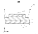
図13は、第3実施形態における半導体装置300の製造方法を示す工程図である。まず、製造者は、第1実施形態と同様に、表面117およびトレンチ128を有する半導体層112,114,116を形成する(工程P310)。これによって、製造者は、トレンチ128が形成された半導体装置100bを得る(図5)。
以上説明した第3実施形態によれば、第1実施形態と同様に、製造コストの抑制および素子の微細化を実現しながら、ソース電極141のオーミック性を十分に確保できる。また、第2実施形態と同様に、絶縁層331の特性と絶縁層332の特性との組み合わせによって、絶縁膜330に要求される特性を実現できる。また、ソース電極141を形成する処理(工程P330)による汚染から、トレンチ128における半導体層114の表面を絶縁層331によって保護できるため、トレンチ128における半導体層114と絶縁膜330との間における界面準位密度の増加に伴う界面特性の悪化を抑制できる。また、自己整合によってソース電極141を形成できるため、設計マージンによる素子寸法の拡大を抑制できる。また、自己整合によって、ソース電極141を形成するマスクを別途作製する必要がないため、製造コストを抑制できる。
D−1.半導体装置の構成
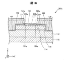
図19は、第4実施形態における半導体装置400の構成を模式的に示す断面図である。第4実施形態における半導体装置400の構成は、ボディ電極444を形成するために各部の構造が異なる点を除き、第1実施形態の半導体装置100と同様である。半導体装置400は、半導体装置100と異なる構成として、リセス429と、ボディ電極444と、絶縁膜430と、ソース電極441と、保護電極443とを備える。
図20は、第4実施形態における半導体装置400の製造方法を示す工程図である。まず、製造者は、MOCVDを用いて基板110の上に半導体層112,114,116を順に形成した後、ドライエッチングによってトレンチ128およびリセス429を形成する(工程P410)。
以上説明した第4実施形態によれば、第1実施形態と同様に、製造コストの抑制および素子の微細化を実現しながら、ソース電極441のオーミック性を十分に確保できる。また、ボディ電極444によってボディーダイオードを形成できる。
図21は、第5実施形態における半導体装置500の構成を模式的に示す断面図である。第5実施形態における半導体装置500の構成は、ボディ電極444を形成するために各部の構造が異なる点を除き、第1実施形態の半導体装置100と同様である。半導体装置500は、半導体装置100と異なる構成として、リセス429と、ボディ電極444と、絶縁膜530と、ソース電極541と、保護電極543とを備える。半導体装置500のリセス429およびボディ電極444は、第4実施形態と同様である。
図22は、第6実施形態における半導体装置600の構成を示す断面図である。第6実施形態における半導体装置600の構成は、絶縁膜630を備える点を除き、第5実施形態の半導体装置500と同様である。半導体装置600の絶縁膜630は、ボディ電極444の外縁端444eより内側に開口端630pを有する点を除き、第5実施形態の絶縁膜530と同様である。
G−1.半導体装置の構成
図23は、第7実施形態における半導体装置700の構成を示す断面図である。第7実施形態における半導体装置700の構成は、絶縁膜730を備える点を除き、第5実施形態の半導体装置500と同様である。半導体装置700の絶縁膜730は、2層の絶縁層731,732から成る多層構造を有する。他の実施形態では、絶縁膜730は、3層以上の絶縁層から成る多層構造を有してもよい。
図24は、第7実施形態における半導体装置700の製造方法を示す工程図である。まず、製造者は、MOCVDを用いて基板110の上に半導体層112,114,116を順に形成した後、ドライエッチングによってトレンチ128およびリセス429を形成する(工程P710)。
以上説明した第7実施形態によれば、第1実施形態と同様に、製造コストの抑制および素子の微細化を実現しながら、ソース電極541のオーミック性を十分に確保できる。また、第2実施形態と同様に、絶縁層731の特性と絶縁層732の特性との組み合わせによって、絶縁膜730に要求される特性を実現できる。また、ソース電極541を形成する処理(工程P330)による汚染から、トレンチ128における半導体層114の表面を絶縁層731によって保護できるため、トレンチ128における半導体層114と絶縁膜730との間における界面準位密度の増加に伴う界面特性の悪化を抑制できる。また、自己整合によってソース電極541を形成できるため、設計マージンによる素子寸法の拡大を抑制できる。また、自己整合によって、ソース電極541を形成するマスクを別途作製する必要がないため、製造コストを抑制できる。
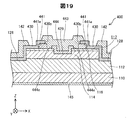
図25は、第8実施形態における半導体装置800の構成を模式的に示す断面図である。図25には、図1と同様にXYZ軸が図示されている。半導体装置800は、GaN系の半導体装置である。本実施形態では、半導体装置800は、リセス構造を有する横型MISFET(Metal-Insulator-Semiconductor Field-Effect Transistor)である。
図26は、第9実施形態における半導体装置900の構成を模式的に示す断面図である。図26には、図1と同様にXYZ軸が図示されている。半導体装置900は、GaN系の半導体装置である。本実施形態では、半導体装置900は、横型HFET(Heterostructure Field-Effect Transistor)である。
本発明は、上述の実施形態や実施例、変形例に限られるものではなく、その趣旨を逸脱しない範囲において種々の構成で実現することができる。例えば、発明の概要の欄に記載した各形態中の技術的特徴に対応する実施形態、実施例、変形例中の技術的特徴は、上述の課題の一部または全部を解決するために、あるいは、上述の効果の一部または全部を達成するために、適宜、差し替えや、組み合わせを行うことが可能である。また、その技術的特徴が本明細書中に必須なものとして説明されていなければ、適宜、削除することが可能である。
110…基板
112…半導体層
114…半導体層(p型半導体層)
116…半導体層(n型半導体層)
117…表面
128…トレンチ
130…絶縁膜
130p…開口端
131p…開口端
141…ソース電極
141e…外縁端
142…ゲート電極
143…保護電極
143e…外縁端
145…ドレイン電極
148…電極層
200…半導体装置
230…絶縁膜
231,232…絶縁層
300,300a〜300e…半導体装置
330…絶縁膜
331,332…絶縁層
392…マスク
392p…開口端
400…半導体装置
429…リセス
430…絶縁膜
430p…開口端
441…ソース電極
441e…外縁端
443…保護電極
444…ボディ電極
444e…外縁端
500…半導体装置
530…絶縁膜
530p…開口端
541…ソース電極
541e…外縁端
543…保護電極
600…半導体装置
630…絶縁膜
630p…開口端
700…半導体装置
730…絶縁膜
730p…開口端
731,732…絶縁層
800…半導体装置
810…基板
812,814,816…半導体層
817…表面
828…リセス
830…絶縁膜
831p,835p…開口端
841…ソース電極
841e…外縁端
842…ゲート電極
843…保護電極
843e…外縁端
844…保護電極
844e…外縁端
845…ドレイン電極
845e…外縁端
900…半導体装置
930…絶縁膜
932p…開口端
942…ゲート電極
Claims (12)
- 半導体装置であって、
半導体層と、
前記半導体層の一部にオーミック接触する第1の電極と、
前記半導体層の上から前記第1の電極の上にわたって形成され、前記第1の電極の外縁端より内側に開口部を有する絶縁膜と、
前記第1の電極とは異なる位置において、前記絶縁膜および前記半導体層の少なくとも一方の上に形成された第2の電極と、
前記第2の電極を構成する成分と同一の成分から成り、前記開口部を通じて前記第1の電極の上に形成されるとともに、前記第1の電極の上から前記絶縁膜上における前記第1の電極の前記外縁端より内側にわたって形成された第3の電極と
を備える半導体装置。 - 請求項1に記載の半導体装置であって、
前記絶縁膜は、
前記半導体層の上から前記第1の電極の上にわたって形成された第1の絶縁層と、
前記第1の絶縁層の上に形成された第2の絶縁層と
を含む、半導体装置。 - 請求項1に記載の半導体装置であって、
前記絶縁膜は、
前記半導体層の上に形成された第1の絶縁層と、
前記第1の絶縁層の上から前記第1の電極の上にわたって形成された第2の絶縁層と
を含む、半導体装置。 - 前記第1の絶縁層を構成する成分は、前記第2の絶縁層を構成する成分とは異なる、請求項2または請求項3に記載の半導体装置。
- 請求項1から請求項4までのいずれか一項に記載の半導体装置であって、
前記第1の電極は、ソース電極であり、
前記第2の電極は、ゲート電極である、半導体装置。 - 請求項1から請求項5までのいずれか一項に記載の半導体装置であって、
前記半導体層は、
p型半導体層と、
前記p型半導体層に隣接し、前記第1の電極が形成された表面を有するn型半導体層と
を含み、
前記p型半導体層の上に形成された第4の電極を更に備える半導体装置。 - 前記第1の電極は、前記第4の電極に接触する、請求項6に記載の半導体装置。
- 前記絶縁膜の前記開口部は、前記第4の電極の外縁端より内側に位置する、請求項7に記載の半導体装置。
- 前記半導体層は、窒化ガリウム(GaN)から主に成る、請求項1から請求項8までのいずれか一項に記載の半導体装置。
- 半導体装置の製造方法であって、
半導体層を形成し、
前記半導体層の一部にオーミック接触する第1の電極を形成し、
前記半導体層の上から前記第1の電極の上にわたって絶縁膜を形成し、
前記第1の電極の外縁端より内側において前記第1の電極を露出させる開口部を、前記絶縁膜に形成し、
前記絶縁膜の上から前記第1の電極の上にわたって電極層を形成し、
ドライエッチングによって前記電極層を、前記第1の電極とは異なる位置において、前記絶縁膜および前記半導体層の少なくとも一方の上に形成された第2の電極と、前記第1の電極の上から前記絶縁膜上における前記第1の電極の前記外縁端より内側にわたって形成された第3の電極とに分断する、半導体装置の製造方法。 - 請求項10に記載の半導体装置の製造方法であって、
前記第1の電極を形成する前に、前記絶縁膜の一部として、前記半導体層の上に第1の絶縁層を形成し、
前記半導体層を露出させる第1の開口部を前記第1の絶縁層に形成し、
前記第1の開口部から露出する前記半導体層の上に前記第1の電極を形成し、
前記第1の絶縁層の上から前記第1の電極の上にわたって、前記絶縁膜の一部として、第2の絶縁層を形成し、
前記開口部として第2の開口部を前記第2の絶縁層に形成する、半導体装置の製造方法。 - 前記第1の開口部を形成するマスクを、前記第1の電極を形成するマスクとして利用する、請求項11に記載の半導体装置の製造方法。
Priority Applications (3)
| Application Number | Priority Date | Filing Date | Title |
|---|---|---|---|
| JP2014196498A JP6194869B2 (ja) | 2014-09-26 | 2014-09-26 | 半導体装置およびその製造方法 |
| US14/853,867 US9831311B2 (en) | 2014-09-26 | 2015-09-14 | Semiconductor device and method of manufacturing the same |
| CN201510612562.6A CN105470304B (zh) | 2014-09-26 | 2015-09-23 | 半导体装置及其制造方法 |
Applications Claiming Priority (1)
| Application Number | Priority Date | Filing Date | Title |
|---|---|---|---|
| JP2014196498A JP6194869B2 (ja) | 2014-09-26 | 2014-09-26 | 半導体装置およびその製造方法 |
Publications (3)
| Publication Number | Publication Date |
|---|---|
| JP2016072265A JP2016072265A (ja) | 2016-05-09 |
| JP2016072265A5 JP2016072265A5 (ja) | 2017-01-12 |
| JP6194869B2 true JP6194869B2 (ja) | 2017-09-13 |
Family
ID=55585341
Family Applications (1)
| Application Number | Title | Priority Date | Filing Date |
|---|---|---|---|
| JP2014196498A Active JP6194869B2 (ja) | 2014-09-26 | 2014-09-26 | 半導体装置およびその製造方法 |
Country Status (3)
| Country | Link |
|---|---|
| US (1) | US9831311B2 (ja) |
| JP (1) | JP6194869B2 (ja) |
| CN (1) | CN105470304B (ja) |
Families Citing this family (2)
| Publication number | Priority date | Publication date | Assignee | Title |
|---|---|---|---|---|
| JP6791083B2 (ja) * | 2017-09-28 | 2020-11-25 | 豊田合成株式会社 | 半導体装置の製造方法 |
| JP6927116B2 (ja) * | 2018-03-28 | 2021-08-25 | 豊田合成株式会社 | 半導体装置 |
Family Cites Families (11)
| Publication number | Priority date | Publication date | Assignee | Title |
|---|---|---|---|---|
| GB2103419A (en) * | 1981-08-04 | 1983-02-16 | Siliconix Inc | Field effect transistor with metal source |
| JPS6237965A (ja) * | 1985-08-13 | 1987-02-18 | Tdk Corp | 縦形半導体装置およびその製造方法 |
| JPH023980A (ja) * | 1988-06-22 | 1990-01-09 | Nissan Motor Co Ltd | 縦型電界効果トランジスタ |
| JPH06120356A (ja) * | 1992-10-01 | 1994-04-28 | Fujitsu Ltd | 半導体装置及びその製造方法 |
| JP3154364B2 (ja) | 1994-01-28 | 2001-04-09 | 日亜化学工業株式会社 | n型窒化ガリウム系化合物半導体層の電極及びその形成方法 |
| EP0622858B2 (en) | 1993-04-28 | 2004-09-29 | Nichia Corporation | Gallium nitride-based III-V group compound semiconductor device and method of producing the same |
| JP2637937B2 (ja) * | 1995-01-30 | 1997-08-06 | 関西日本電気株式会社 | 電界効果トランジスタの製造方法 |
| JP5420157B2 (ja) * | 2007-06-08 | 2014-02-19 | 住友電工デバイス・イノベーション株式会社 | 半導体装置の製造方法 |
| US9099433B2 (en) * | 2012-04-23 | 2015-08-04 | Freescale Semiconductor, Inc. | High speed gallium nitride transistor devices |
| JP6007769B2 (ja) * | 2012-12-14 | 2016-10-12 | 豊田合成株式会社 | 半導体装置 |
| US9685345B2 (en) * | 2013-11-19 | 2017-06-20 | Nxp Usa, Inc. | Semiconductor devices with integrated Schottky diodes and methods of fabrication |
-
2014
- 2014-09-26 JP JP2014196498A patent/JP6194869B2/ja active Active
-
2015
- 2015-09-14 US US14/853,867 patent/US9831311B2/en active Active
- 2015-09-23 CN CN201510612562.6A patent/CN105470304B/zh active Active
Also Published As
| Publication number | Publication date |
|---|---|
| CN105470304B (zh) | 2018-09-14 |
| US20160093703A1 (en) | 2016-03-31 |
| US9831311B2 (en) | 2017-11-28 |
| CN105470304A (zh) | 2016-04-06 |
| JP2016072265A (ja) | 2016-05-09 |
Similar Documents
| Publication | Publication Date | Title |
|---|---|---|
| KR102065115B1 (ko) | E-모드를 갖는 고 전자 이동도 트랜지스터 및 그 제조방법 | |
| JP6341077B2 (ja) | 半導体装置の製造方法 | |
| JP5597581B2 (ja) | 窒化物半導体装置及びその製造方法 | |
| TW201830707A (zh) | 半導體裝置之製造方法 | |
| US10784361B2 (en) | Semiconductor device and method for manufacturing the same | |
| JP2008277640A (ja) | 窒化物半導体素子 | |
| JP2011198837A (ja) | 半導体装置およびその製造方法 | |
| JP6272557B2 (ja) | 窒化物半導体電界効果トランジスタ | |
| JP5468301B2 (ja) | 窒化物半導体装置および窒化物半導体装置製造方法 | |
| US10243049B2 (en) | Nitride semiconductor device | |
| KR20210074871A (ko) | 반도체 장치 및 그 제조 방법 | |
| JP5827529B2 (ja) | 窒化物半導体装置およびその製造方法 | |
| JP2014045174A (ja) | 窒化物半導体装置 | |
| JP6762977B2 (ja) | 半導体装置、半導体装置の製造方法、電源回路、及び、コンピュータ | |
| US10497572B2 (en) | Method for manufacturing semiconductor device | |
| WO2014003047A1 (ja) | 窒化物半導体装置の電極構造およびその製造方法並びに窒化物半導体電界効果トランジスタ | |
| US10629475B2 (en) | Semiconductor device with two-part insulation structure within non-active region | |
| JP6194869B2 (ja) | 半導体装置およびその製造方法 | |
| JP6406080B2 (ja) | 半導体装置の製造方法 | |
| CN110459473B (zh) | 半导体装置及其制造方法 | |
| JP6422909B2 (ja) | 半導体装置 | |
| US9893210B2 (en) | Semiconductor device and method of manufacturing the same | |
| JP6327139B2 (ja) | 半導体装置およびその製造方法 | |
| JP6176677B2 (ja) | 窒化物半導体装置 | |
| JP6221859B2 (ja) | 半導体装置の製造方法 |
Legal Events
| Date | Code | Title | Description |
|---|---|---|---|
| A621 | Written request for application examination |
Free format text: JAPANESE INTERMEDIATE CODE: A621 Effective date: 20161021 |
|
| A521 | Written amendment |
Free format text: JAPANESE INTERMEDIATE CODE: A523 Effective date: 20161125 |
|
| A977 | Report on retrieval |
Free format text: JAPANESE INTERMEDIATE CODE: A971007 Effective date: 20170712 |
|
| TRDD | Decision of grant or rejection written | ||
| A01 | Written decision to grant a patent or to grant a registration (utility model) |
Free format text: JAPANESE INTERMEDIATE CODE: A01 Effective date: 20170718 |
|
| A61 | First payment of annual fees (during grant procedure) |
Free format text: JAPANESE INTERMEDIATE CODE: A61 Effective date: 20170731 |
|
| R150 | Certificate of patent or registration of utility model |
Ref document number: 6194869 Country of ref document: JP Free format text: JAPANESE INTERMEDIATE CODE: R150 |