JP6186380B2 - 半導体層に対するオーミックコンタクトを含むデバイスヘテロ構造を形成することを含む方法および半導体層に対するオーミックコンタクトを含むデバイスヘテロ構造を含むデバイス - Google Patents
半導体層に対するオーミックコンタクトを含むデバイスヘテロ構造を形成することを含む方法および半導体層に対するオーミックコンタクトを含むデバイスヘテロ構造を含むデバイス Download PDFInfo
- Publication number
- JP6186380B2 JP6186380B2 JP2014558905A JP2014558905A JP6186380B2 JP 6186380 B2 JP6186380 B2 JP 6186380B2 JP 2014558905 A JP2014558905 A JP 2014558905A JP 2014558905 A JP2014558905 A JP 2014558905A JP 6186380 B2 JP6186380 B2 JP 6186380B2
- Authority
- JP
- Japan
- Prior art keywords
- semiconductor layers
- semiconductor layer
- forming
- layer
- highly conductive
- Prior art date
- Legal status (The legal status is an assumption and is not a legal conclusion. Google has not performed a legal analysis and makes no representation as to the accuracy of the status listed.)
- Active
Links
- 239000004065 semiconductor Substances 0.000 title claims description 185
- 238000000034 method Methods 0.000 title claims description 54
- 239000000463 material Substances 0.000 claims description 62
- 230000000873 masking effect Effects 0.000 claims description 21
- 229910052782 aluminium Inorganic materials 0.000 claims description 13
- XAGFODPZIPBFFR-UHFFFAOYSA-N aluminium Chemical compound [Al] XAGFODPZIPBFFR-UHFFFAOYSA-N 0.000 claims description 11
- 150000004767 nitrides Chemical class 0.000 claims description 11
- 238000005530 etching Methods 0.000 claims description 10
- 229910052738 indium Inorganic materials 0.000 claims description 7
- APFVFJFRJDLVQX-UHFFFAOYSA-N indium atom Chemical compound [In] APFVFJFRJDLVQX-UHFFFAOYSA-N 0.000 claims description 7
- 238000012545 processing Methods 0.000 claims description 7
- 238000009825 accumulation Methods 0.000 claims description 3
- 230000001939 inductive effect Effects 0.000 claims description 3
- 230000002441 reversible effect Effects 0.000 claims description 3
- 229910052751 metal Inorganic materials 0.000 description 38
- 239000002184 metal Substances 0.000 description 38
- 238000004519 manufacturing process Methods 0.000 description 18
- 238000013461 design Methods 0.000 description 17
- 238000005253 cladding Methods 0.000 description 16
- 229910002601 GaN Inorganic materials 0.000 description 10
- JMASRVWKEDWRBT-UHFFFAOYSA-N Gallium nitride Chemical compound [Ga]#N JMASRVWKEDWRBT-UHFFFAOYSA-N 0.000 description 10
- 239000011651 chromium Substances 0.000 description 10
- 239000010931 gold Substances 0.000 description 10
- 239000000758 substrate Substances 0.000 description 10
- 239000010936 titanium Substances 0.000 description 10
- 238000001020 plasma etching Methods 0.000 description 8
- 230000005670 electromagnetic radiation Effects 0.000 description 7
- 230000005855 radiation Effects 0.000 description 7
- 238000013459 approach Methods 0.000 description 6
- 230000015572 biosynthetic process Effects 0.000 description 6
- 229910052804 chromium Inorganic materials 0.000 description 6
- 229910052737 gold Inorganic materials 0.000 description 6
- 239000000203 mixture Substances 0.000 description 6
- VYPSYNLAJGMNEJ-UHFFFAOYSA-N silicon dioxide Inorganic materials O=[Si]=O VYPSYNLAJGMNEJ-UHFFFAOYSA-N 0.000 description 5
- PXHVJJICTQNCMI-UHFFFAOYSA-N Nickel Chemical compound [Ni] PXHVJJICTQNCMI-UHFFFAOYSA-N 0.000 description 4
- 238000004590 computer program Methods 0.000 description 4
- PMHQVHHXPFUNSP-UHFFFAOYSA-M copper(1+);methylsulfanylmethane;bromide Chemical compound Br[Cu].CSC PMHQVHHXPFUNSP-UHFFFAOYSA-M 0.000 description 4
- 238000000151 deposition Methods 0.000 description 4
- 230000001771 impaired effect Effects 0.000 description 4
- BASFCYQUMIYNBI-UHFFFAOYSA-N platinum Chemical compound [Pt] BASFCYQUMIYNBI-UHFFFAOYSA-N 0.000 description 4
- 208000012868 Overgrowth Diseases 0.000 description 3
- RNQKDQAVIXDKAG-UHFFFAOYSA-N aluminum gallium Chemical compound [Al].[Ga] RNQKDQAVIXDKAG-UHFFFAOYSA-N 0.000 description 3
- 238000000137 annealing Methods 0.000 description 3
- 229910052733 gallium Inorganic materials 0.000 description 3
- 150000002500 ions Chemical class 0.000 description 3
- 150000002739 metals Chemical class 0.000 description 3
- 229910052757 nitrogen Inorganic materials 0.000 description 3
- 235000012239 silicon dioxide Nutrition 0.000 description 3
- 239000000377 silicon dioxide Substances 0.000 description 3
- 229910016455 AlBN Inorganic materials 0.000 description 2
- IJGRMHOSHXDMSA-UHFFFAOYSA-N Atomic nitrogen Chemical compound N#N IJGRMHOSHXDMSA-UHFFFAOYSA-N 0.000 description 2
- GYHNNYVSQQEPJS-UHFFFAOYSA-N Gallium Chemical compound [Ga] GYHNNYVSQQEPJS-UHFFFAOYSA-N 0.000 description 2
- 229910001199 N alloy Inorganic materials 0.000 description 2
- 229910004298 SiO 2 Inorganic materials 0.000 description 2
- XUIMIQQOPSSXEZ-UHFFFAOYSA-N Silicon Chemical compound [Si] XUIMIQQOPSSXEZ-UHFFFAOYSA-N 0.000 description 2
- 230000004888 barrier function Effects 0.000 description 2
- 230000001010 compromised effect Effects 0.000 description 2
- 238000010586 diagram Methods 0.000 description 2
- 238000000605 extraction Methods 0.000 description 2
- 239000011777 magnesium Substances 0.000 description 2
- 238000012986 modification Methods 0.000 description 2
- 230000004048 modification Effects 0.000 description 2
- 230000003287 optical effect Effects 0.000 description 2
- 230000000737 periodic effect Effects 0.000 description 2
- 238000000206 photolithography Methods 0.000 description 2
- 229910052594 sapphire Inorganic materials 0.000 description 2
- 239000010980 sapphire Substances 0.000 description 2
- HBMJWWWQQXIZIP-UHFFFAOYSA-N silicon carbide Chemical compound [Si+]#[C-] HBMJWWWQQXIZIP-UHFFFAOYSA-N 0.000 description 2
- 230000001502 supplementing effect Effects 0.000 description 2
- 229910052719 titanium Inorganic materials 0.000 description 2
- 229910017109 AlON Inorganic materials 0.000 description 1
- PIGFYZPCRLYGLF-UHFFFAOYSA-N Aluminum nitride Chemical compound [Al]#N PIGFYZPCRLYGLF-UHFFFAOYSA-N 0.000 description 1
- ZOXJGFHDIHLPTG-UHFFFAOYSA-N Boron Chemical compound [B] ZOXJGFHDIHLPTG-UHFFFAOYSA-N 0.000 description 1
- VYZAMTAEIAYCRO-UHFFFAOYSA-N Chromium Chemical compound [Cr] VYZAMTAEIAYCRO-UHFFFAOYSA-N 0.000 description 1
- FYYHWMGAXLPEAU-UHFFFAOYSA-N Magnesium Chemical compound [Mg] FYYHWMGAXLPEAU-UHFFFAOYSA-N 0.000 description 1
- 229910052581 Si3N4 Inorganic materials 0.000 description 1
- RTAQQCXQSZGOHL-UHFFFAOYSA-N Titanium Chemical compound [Ti] RTAQQCXQSZGOHL-UHFFFAOYSA-N 0.000 description 1
- 239000000956 alloy Substances 0.000 description 1
- 229910045601 alloy Inorganic materials 0.000 description 1
- NWAIGJYBQQYSPW-UHFFFAOYSA-N azanylidyneindigane Chemical compound [In]#N NWAIGJYBQQYSPW-UHFFFAOYSA-N 0.000 description 1
- 230000000903 blocking effect Effects 0.000 description 1
- 229910052796 boron Inorganic materials 0.000 description 1
- 238000005219 brazing Methods 0.000 description 1
- 239000000969 carrier Substances 0.000 description 1
- 239000012159 carrier gas Substances 0.000 description 1
- 230000015556 catabolic process Effects 0.000 description 1
- 238000005229 chemical vapour deposition Methods 0.000 description 1
- 229910017052 cobalt Inorganic materials 0.000 description 1
- 239000010941 cobalt Substances 0.000 description 1
- GUTLYIVDDKVIGB-UHFFFAOYSA-N cobalt atom Chemical compound [Co] GUTLYIVDDKVIGB-UHFFFAOYSA-N 0.000 description 1
- 238000004891 communication Methods 0.000 description 1
- 230000007547 defect Effects 0.000 description 1
- 230000008021 deposition Effects 0.000 description 1
- 238000011161 development Methods 0.000 description 1
- 239000002019 doping agent Substances 0.000 description 1
- 238000004070 electrodeposition Methods 0.000 description 1
- 238000005566 electron beam evaporation Methods 0.000 description 1
- 238000009713 electroplating Methods 0.000 description 1
- 238000005516 engineering process Methods 0.000 description 1
- 230000005669 field effect Effects 0.000 description 1
- 229910052732 germanium Inorganic materials 0.000 description 1
- GNPVGFCGXDBREM-UHFFFAOYSA-N germanium atom Chemical compound [Ge] GNPVGFCGXDBREM-UHFFFAOYSA-N 0.000 description 1
- PCHJSUWPFVWCPO-UHFFFAOYSA-N gold Chemical compound [Au] PCHJSUWPFVWCPO-UHFFFAOYSA-N 0.000 description 1
- 238000009434 installation Methods 0.000 description 1
- 229910052749 magnesium Inorganic materials 0.000 description 1
- 230000008018 melting Effects 0.000 description 1
- 238000002844 melting Methods 0.000 description 1
- 239000002105 nanoparticle Substances 0.000 description 1
- 229910052759 nickel Inorganic materials 0.000 description 1
- 230000006911 nucleation Effects 0.000 description 1
- 238000010899 nucleation Methods 0.000 description 1
- 238000002161 passivation Methods 0.000 description 1
- 229920002120 photoresistant polymer Polymers 0.000 description 1
- 229910052697 platinum Inorganic materials 0.000 description 1
- 229910052710 silicon Inorganic materials 0.000 description 1
- 239000010703 silicon Substances 0.000 description 1
- HQVNEWCFYHHQES-UHFFFAOYSA-N silicon nitride Chemical compound N12[Si]34N5[Si]62N3[Si]51N64 HQVNEWCFYHHQES-UHFFFAOYSA-N 0.000 description 1
- 230000026676 system process Effects 0.000 description 1
- 238000002207 thermal evaporation Methods 0.000 description 1
- 239000012780 transparent material Substances 0.000 description 1
- 230000005533 two-dimensional electron gas Effects 0.000 description 1
Images


Classifications
-
- H—ELECTRICITY
- H01—ELECTRIC ELEMENTS
- H01L—SEMICONDUCTOR DEVICES NOT COVERED BY CLASS H10
- H01L29/00—Semiconductor devices specially adapted for rectifying, amplifying, oscillating or switching and having potential barriers; Capacitors or resistors having potential barriers, e.g. a PN-junction depletion layer or carrier concentration layer; Details of semiconductor bodies or of electrodes thereof ; Multistep manufacturing processes therefor
- H01L29/40—Electrodes ; Multistep manufacturing processes therefor
- H01L29/43—Electrodes ; Multistep manufacturing processes therefor characterised by the materials of which they are formed
- H01L29/45—Ohmic electrodes
- H01L29/452—Ohmic electrodes on AIII-BV compounds
-
- H—ELECTRICITY
- H01—ELECTRIC ELEMENTS
- H01L—SEMICONDUCTOR DEVICES NOT COVERED BY CLASS H10
- H01L21/00—Processes or apparatus adapted for the manufacture or treatment of semiconductor or solid state devices or of parts thereof
- H01L21/02—Manufacture or treatment of semiconductor devices or of parts thereof
- H01L21/04—Manufacture or treatment of semiconductor devices or of parts thereof the devices having potential barriers, e.g. a PN junction, depletion layer or carrier concentration layer
- H01L21/18—Manufacture or treatment of semiconductor devices or of parts thereof the devices having potential barriers, e.g. a PN junction, depletion layer or carrier concentration layer the devices having semiconductor bodies comprising elements of Group IV of the Periodic Table or AIIIBV compounds with or without impurities, e.g. doping materials
- H01L21/28—Manufacture of electrodes on semiconductor bodies using processes or apparatus not provided for in groups H01L21/20 - H01L21/268
- H01L21/283—Deposition of conductive or insulating materials for electrodes conducting electric current
- H01L21/285—Deposition of conductive or insulating materials for electrodes conducting electric current from a gas or vapour, e.g. condensation
- H01L21/28506—Deposition of conductive or insulating materials for electrodes conducting electric current from a gas or vapour, e.g. condensation of conductive layers
- H01L21/28575—Deposition of conductive or insulating materials for electrodes conducting electric current from a gas or vapour, e.g. condensation of conductive layers on semiconductor bodies comprising AIIIBV compounds
-
- H—ELECTRICITY
- H01—ELECTRIC ELEMENTS
- H01L—SEMICONDUCTOR DEVICES NOT COVERED BY CLASS H10
- H01L29/00—Semiconductor devices specially adapted for rectifying, amplifying, oscillating or switching and having potential barriers; Capacitors or resistors having potential barriers, e.g. a PN-junction depletion layer or carrier concentration layer; Details of semiconductor bodies or of electrodes thereof ; Multistep manufacturing processes therefor
- H01L29/02—Semiconductor bodies ; Multistep manufacturing processes therefor
- H01L29/12—Semiconductor bodies ; Multistep manufacturing processes therefor characterised by the materials of which they are formed
- H01L29/15—Structures with periodic or quasi periodic potential variation, e.g. multiple quantum wells, superlattices
- H01L29/151—Compositional structures
- H01L29/152—Compositional structures with quantum effects only in vertical direction, i.e. layered structures with quantum effects solely resulting from vertical potential variation
- H01L29/155—Comprising only semiconductor materials
-
- H—ELECTRICITY
- H01—ELECTRIC ELEMENTS
- H01L—SEMICONDUCTOR DEVICES NOT COVERED BY CLASS H10
- H01L29/00—Semiconductor devices specially adapted for rectifying, amplifying, oscillating or switching and having potential barriers; Capacitors or resistors having potential barriers, e.g. a PN-junction depletion layer or carrier concentration layer; Details of semiconductor bodies or of electrodes thereof ; Multistep manufacturing processes therefor
- H01L29/02—Semiconductor bodies ; Multistep manufacturing processes therefor
- H01L29/12—Semiconductor bodies ; Multistep manufacturing processes therefor characterised by the materials of which they are formed
- H01L29/20—Semiconductor bodies ; Multistep manufacturing processes therefor characterised by the materials of which they are formed including, apart from doping materials or other impurities, only AIIIBV compounds
- H01L29/2003—Nitride compounds
-
- H—ELECTRICITY
- H01—ELECTRIC ELEMENTS
- H01L—SEMICONDUCTOR DEVICES NOT COVERED BY CLASS H10
- H01L29/00—Semiconductor devices specially adapted for rectifying, amplifying, oscillating or switching and having potential barriers; Capacitors or resistors having potential barriers, e.g. a PN-junction depletion layer or carrier concentration layer; Details of semiconductor bodies or of electrodes thereof ; Multistep manufacturing processes therefor
- H01L29/02—Semiconductor bodies ; Multistep manufacturing processes therefor
- H01L29/12—Semiconductor bodies ; Multistep manufacturing processes therefor characterised by the materials of which they are formed
- H01L29/20—Semiconductor bodies ; Multistep manufacturing processes therefor characterised by the materials of which they are formed including, apart from doping materials or other impurities, only AIIIBV compounds
- H01L29/201—Semiconductor bodies ; Multistep manufacturing processes therefor characterised by the materials of which they are formed including, apart from doping materials or other impurities, only AIIIBV compounds including two or more compounds, e.g. alloys
- H01L29/205—Semiconductor bodies ; Multistep manufacturing processes therefor characterised by the materials of which they are formed including, apart from doping materials or other impurities, only AIIIBV compounds including two or more compounds, e.g. alloys in different semiconductor regions, e.g. heterojunctions
-
- H—ELECTRICITY
- H01—ELECTRIC ELEMENTS
- H01L—SEMICONDUCTOR DEVICES NOT COVERED BY CLASS H10
- H01L29/00—Semiconductor devices specially adapted for rectifying, amplifying, oscillating or switching and having potential barriers; Capacitors or resistors having potential barriers, e.g. a PN-junction depletion layer or carrier concentration layer; Details of semiconductor bodies or of electrodes thereof ; Multistep manufacturing processes therefor
- H01L29/40—Electrodes ; Multistep manufacturing processes therefor
- H01L29/401—Multistep manufacturing processes
-
- H—ELECTRICITY
- H01—ELECTRIC ELEMENTS
- H01L—SEMICONDUCTOR DEVICES NOT COVERED BY CLASS H10
- H01L29/00—Semiconductor devices specially adapted for rectifying, amplifying, oscillating or switching and having potential barriers; Capacitors or resistors having potential barriers, e.g. a PN-junction depletion layer or carrier concentration layer; Details of semiconductor bodies or of electrodes thereof ; Multistep manufacturing processes therefor
- H01L29/66—Types of semiconductor device ; Multistep manufacturing processes therefor
- H01L29/66007—Multistep manufacturing processes
- H01L29/66075—Multistep manufacturing processes of devices having semiconductor bodies comprising group 14 or group 13/15 materials
- H01L29/66227—Multistep manufacturing processes of devices having semiconductor bodies comprising group 14 or group 13/15 materials the devices being controllable only by the electric current supplied or the electric potential applied, to an electrode which does not carry the current to be rectified, amplified or switched, e.g. three-terminal devices
- H01L29/66409—Unipolar field-effect transistors
- H01L29/66431—Unipolar field-effect transistors with a heterojunction interface channel or gate, e.g. HFET, HIGFET, SISFET, HJFET, HEMT
-
- H—ELECTRICITY
- H01—ELECTRIC ELEMENTS
- H01L—SEMICONDUCTOR DEVICES NOT COVERED BY CLASS H10
- H01L29/00—Semiconductor devices specially adapted for rectifying, amplifying, oscillating or switching and having potential barriers; Capacitors or resistors having potential barriers, e.g. a PN-junction depletion layer or carrier concentration layer; Details of semiconductor bodies or of electrodes thereof ; Multistep manufacturing processes therefor
- H01L29/66—Types of semiconductor device ; Multistep manufacturing processes therefor
- H01L29/66007—Multistep manufacturing processes
- H01L29/66075—Multistep manufacturing processes of devices having semiconductor bodies comprising group 14 or group 13/15 materials
- H01L29/66227—Multistep manufacturing processes of devices having semiconductor bodies comprising group 14 or group 13/15 materials the devices being controllable only by the electric current supplied or the electric potential applied, to an electrode which does not carry the current to be rectified, amplified or switched, e.g. three-terminal devices
- H01L29/66409—Unipolar field-effect transistors
- H01L29/66446—Unipolar field-effect transistors with an active layer made of a group 13/15 material, e.g. group 13/15 velocity modulation transistor [VMT], group 13/15 negative resistance FET [NERFET]
- H01L29/66462—Unipolar field-effect transistors with an active layer made of a group 13/15 material, e.g. group 13/15 velocity modulation transistor [VMT], group 13/15 negative resistance FET [NERFET] with a heterojunction interface channel or gate, e.g. HFET, HIGFET, SISFET, HJFET, HEMT
-
- H—ELECTRICITY
- H01—ELECTRIC ELEMENTS
- H01L—SEMICONDUCTOR DEVICES NOT COVERED BY CLASS H10
- H01L29/00—Semiconductor devices specially adapted for rectifying, amplifying, oscillating or switching and having potential barriers; Capacitors or resistors having potential barriers, e.g. a PN-junction depletion layer or carrier concentration layer; Details of semiconductor bodies or of electrodes thereof ; Multistep manufacturing processes therefor
- H01L29/66—Types of semiconductor device ; Multistep manufacturing processes therefor
- H01L29/68—Types of semiconductor device ; Multistep manufacturing processes therefor controllable by only the electric current supplied, or only the electric potential applied, to an electrode which does not carry the current to be rectified, amplified or switched
- H01L29/70—Bipolar devices
- H01L29/72—Transistor-type devices, i.e. able to continuously respond to applied control signals
- H01L29/73—Bipolar junction transistors
- H01L29/737—Hetero-junction transistors
-
- H—ELECTRICITY
- H01—ELECTRIC ELEMENTS
- H01L—SEMICONDUCTOR DEVICES NOT COVERED BY CLASS H10
- H01L29/00—Semiconductor devices specially adapted for rectifying, amplifying, oscillating or switching and having potential barriers; Capacitors or resistors having potential barriers, e.g. a PN-junction depletion layer or carrier concentration layer; Details of semiconductor bodies or of electrodes thereof ; Multistep manufacturing processes therefor
- H01L29/66—Types of semiconductor device ; Multistep manufacturing processes therefor
- H01L29/68—Types of semiconductor device ; Multistep manufacturing processes therefor controllable by only the electric current supplied, or only the electric potential applied, to an electrode which does not carry the current to be rectified, amplified or switched
- H01L29/76—Unipolar devices, e.g. field effect transistors
- H01L29/772—Field effect transistors
- H01L29/778—Field effect transistors with two-dimensional charge carrier gas channel, e.g. HEMT ; with two-dimensional charge-carrier layer formed at a heterojunction interface
- H01L29/7786—Field effect transistors with two-dimensional charge carrier gas channel, e.g. HEMT ; with two-dimensional charge-carrier layer formed at a heterojunction interface with direct single heterostructure, i.e. with wide bandgap layer formed on top of active layer, e.g. direct single heterostructure MIS-like HEMT
-
- H—ELECTRICITY
- H01—ELECTRIC ELEMENTS
- H01L—SEMICONDUCTOR DEVICES NOT COVERED BY CLASS H10
- H01L33/00—Semiconductor devices having potential barriers specially adapted for light emission; Processes or apparatus specially adapted for the manufacture or treatment thereof or of parts thereof; Details thereof
- H01L33/0004—Devices characterised by their operation
- H01L33/0008—Devices characterised by their operation having p-n or hi-lo junctions
-
- H—ELECTRICITY
- H01—ELECTRIC ELEMENTS
- H01L—SEMICONDUCTOR DEVICES NOT COVERED BY CLASS H10
- H01L33/00—Semiconductor devices having potential barriers specially adapted for light emission; Processes or apparatus specially adapted for the manufacture or treatment thereof or of parts thereof; Details thereof
- H01L33/005—Processes
- H01L33/0062—Processes for devices with an active region comprising only III-V compounds
- H01L33/0066—Processes for devices with an active region comprising only III-V compounds with a substrate not being a III-V compound
- H01L33/007—Processes for devices with an active region comprising only III-V compounds with a substrate not being a III-V compound comprising nitride compounds
-
- H—ELECTRICITY
- H01—ELECTRIC ELEMENTS
- H01L—SEMICONDUCTOR DEVICES NOT COVERED BY CLASS H10
- H01L33/00—Semiconductor devices having potential barriers specially adapted for light emission; Processes or apparatus specially adapted for the manufacture or treatment thereof or of parts thereof; Details thereof
- H01L33/005—Processes
- H01L33/0062—Processes for devices with an active region comprising only III-V compounds
- H01L33/0075—Processes for devices with an active region comprising only III-V compounds comprising nitride compounds
-
- H—ELECTRICITY
- H01—ELECTRIC ELEMENTS
- H01L—SEMICONDUCTOR DEVICES NOT COVERED BY CLASS H10
- H01L33/00—Semiconductor devices having potential barriers specially adapted for light emission; Processes or apparatus specially adapted for the manufacture or treatment thereof or of parts thereof; Details thereof
- H01L33/02—Semiconductor devices having potential barriers specially adapted for light emission; Processes or apparatus specially adapted for the manufacture or treatment thereof or of parts thereof; Details thereof characterised by the semiconductor bodies
- H01L33/04—Semiconductor devices having potential barriers specially adapted for light emission; Processes or apparatus specially adapted for the manufacture or treatment thereof or of parts thereof; Details thereof characterised by the semiconductor bodies with a quantum effect structure or superlattice, e.g. tunnel junction
- H01L33/06—Semiconductor devices having potential barriers specially adapted for light emission; Processes or apparatus specially adapted for the manufacture or treatment thereof or of parts thereof; Details thereof characterised by the semiconductor bodies with a quantum effect structure or superlattice, e.g. tunnel junction within the light emitting region, e.g. quantum confinement structure or tunnel barrier
-
- H—ELECTRICITY
- H01—ELECTRIC ELEMENTS
- H01L—SEMICONDUCTOR DEVICES NOT COVERED BY CLASS H10
- H01L33/00—Semiconductor devices having potential barriers specially adapted for light emission; Processes or apparatus specially adapted for the manufacture or treatment thereof or of parts thereof; Details thereof
- H01L33/02—Semiconductor devices having potential barriers specially adapted for light emission; Processes or apparatus specially adapted for the manufacture or treatment thereof or of parts thereof; Details thereof characterised by the semiconductor bodies
- H01L33/14—Semiconductor devices having potential barriers specially adapted for light emission; Processes or apparatus specially adapted for the manufacture or treatment thereof or of parts thereof; Details thereof characterised by the semiconductor bodies with a carrier transport control structure, e.g. highly-doped semiconductor layer or current-blocking structure
-
- H—ELECTRICITY
- H01—ELECTRIC ELEMENTS
- H01L—SEMICONDUCTOR DEVICES NOT COVERED BY CLASS H10
- H01L33/00—Semiconductor devices having potential barriers specially adapted for light emission; Processes or apparatus specially adapted for the manufacture or treatment thereof or of parts thereof; Details thereof
- H01L33/02—Semiconductor devices having potential barriers specially adapted for light emission; Processes or apparatus specially adapted for the manufacture or treatment thereof or of parts thereof; Details thereof characterised by the semiconductor bodies
- H01L33/26—Materials of the light emitting region
- H01L33/30—Materials of the light emitting region containing only elements of Group III and Group V of the Periodic Table
- H01L33/32—Materials of the light emitting region containing only elements of Group III and Group V of the Periodic Table containing nitrogen
-
- H—ELECTRICITY
- H01—ELECTRIC ELEMENTS
- H01L—SEMICONDUCTOR DEVICES NOT COVERED BY CLASS H10
- H01L33/00—Semiconductor devices having potential barriers specially adapted for light emission; Processes or apparatus specially adapted for the manufacture or treatment thereof or of parts thereof; Details thereof
- H01L33/36—Semiconductor devices having potential barriers specially adapted for light emission; Processes or apparatus specially adapted for the manufacture or treatment thereof or of parts thereof; Details thereof characterised by the electrodes
- H01L33/40—Materials therefor
- H01L33/405—Reflective materials
-
- H—ELECTRICITY
- H01—ELECTRIC ELEMENTS
- H01L—SEMICONDUCTOR DEVICES NOT COVERED BY CLASS H10
- H01L29/00—Semiconductor devices specially adapted for rectifying, amplifying, oscillating or switching and having potential barriers; Capacitors or resistors having potential barriers, e.g. a PN-junction depletion layer or carrier concentration layer; Details of semiconductor bodies or of electrodes thereof ; Multistep manufacturing processes therefor
- H01L29/02—Semiconductor bodies ; Multistep manufacturing processes therefor
- H01L29/12—Semiconductor bodies ; Multistep manufacturing processes therefor characterised by the materials of which they are formed
- H01L29/20—Semiconductor bodies ; Multistep manufacturing processes therefor characterised by the materials of which they are formed including, apart from doping materials or other impurities, only AIIIBV compounds
- H01L29/201—Semiconductor bodies ; Multistep manufacturing processes therefor characterised by the materials of which they are formed including, apart from doping materials or other impurities, only AIIIBV compounds including two or more compounds, e.g. alloys
-
- H—ELECTRICITY
- H01—ELECTRIC ELEMENTS
- H01L—SEMICONDUCTOR DEVICES NOT COVERED BY CLASS H10
- H01L2933/00—Details relating to devices covered by the group H01L33/00 but not provided for in its subgroups
- H01L2933/0008—Processes
- H01L2933/0016—Processes relating to electrodes
-
- H—ELECTRICITY
- H01—ELECTRIC ELEMENTS
- H01L—SEMICONDUCTOR DEVICES NOT COVERED BY CLASS H10
- H01L33/00—Semiconductor devices having potential barriers specially adapted for light emission; Processes or apparatus specially adapted for the manufacture or treatment thereof or of parts thereof; Details thereof
- H01L33/36—Semiconductor devices having potential barriers specially adapted for light emission; Processes or apparatus specially adapted for the manufacture or treatment thereof or of parts thereof; Details thereof characterised by the electrodes
- H01L33/40—Materials therefor
Landscapes
- Engineering & Computer Science (AREA)
- Microelectronics & Electronic Packaging (AREA)
- Power Engineering (AREA)
- Computer Hardware Design (AREA)
- Manufacturing & Machinery (AREA)
- Physics & Mathematics (AREA)
- Condensed Matter Physics & Semiconductors (AREA)
- General Physics & Mathematics (AREA)
- Ceramic Engineering (AREA)
- Electrodes Of Semiconductors (AREA)
- Led Devices (AREA)
Description
本出願は、同時係属中の「Ohmic Contact to Semiconductors and the Process of Producing the Same」の名称において2012年2月23日に出願された米国特許仮出願第61/602,155号の恩典を主張するものであり、なお、当該仮出願は、参照により本明細書に組み入れられる。
Claims (16)
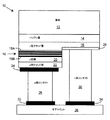
- 半導体層をエッチングすることなく、デバイスヘテロ構造の一セットの半導体層において半導体層に対するオーミックコンタクトを含む前記デバイスヘテロ構造を形成することを含む方法であって、
前記デバイスへテロ構造を形成することは、
前記半導体層の表面上の前記オーミックコンタクトに対応する一セットのコンタクト領域上にマスキング材料を適用し、
前記マスキング材料を適用した後に、前記半導体層の表面の一セットのマスクされていない領域を覆う隆起領域を形成し、
前記一セットのコンタクト領域上に一セットの高導電性半導体層を形成し、
前記隆起領域の形成後に前記一セットの高導電性半導体層上にオーミックコンタクトを形成することを含み、
前記一セットの高導電性半導体層を形成することは、前記一セットのコンタクト領域からの距離に関して前記一セットの高導電性半導体層を形成する材料の少なくとも1つの元素のモル分率に傾斜を持たせることを含み、
前記オーミックコンタクトを形成することは、デバイスヘテロ構造に前記一セットの半導体層のいずれかを形成する材料の品質が損なわれる温度範囲よりも低い処理温度において実施されることを特徴とする方法。 - 前記オーミックコンタクトを形成する前に、前記隆起領域上に少なくとも1つの追加の半導体層を形成することをさらに含む、請求項1に記載の方法。
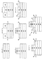
- 前記オーミックコンタクトを形成する前に、前記一セットのコンタクト領域のそれぞれから前記マスキング材料を除去することをさらに含む、請求項1に記載の方法。
- 前記オーミックコンタクトを形成する前に、前記一セットのマスクされていない領域に対応する前記デバイスヘテロ構造の表面にマスキング材料を適用することをさらに含む、請求項1に記載の方法。
- 前記一セットの高導電性半導体層がIII族窒化物材料で形成され、
前記一セットの高導電性半導体層が、前記半導体層と前記一セットの高導電性半導体層との界面において前記半導体層と格子整合される、請求項1に記載の方法。 - 前記一セットの高導電性半導体層を形成することが、前記一セットの高導電性半導体層をデルタドーピングする工程を含む、請求項1に記載の方法。
- 前記一セットの高導電性半導体層が、III族窒化物材料で形成され、
前記傾斜を持たせることが、前記一セットのコンタクト領域から離れる方向にアルミニウムのモル分率が増加することである、請求項1に記載の方法。 - 前記傾斜を持たせることが、前記一セットのコンタクト領域から離れる方向にインジウムのモル分率が減少することである、請求項7に記載の方法。
- 前記一セットのコンタクト領域と前記一セットの高導電性半導体層との界面において、前記アルミニウムのモル分率が0である、請求項7または8に記載の方法。
- 前記傾斜が、前記一セットのコンタクト領域において逆キャリアの蓄積の誘起を避けるように構成される、請求項1に記載の方法。
- 前記デバイスヘテロ構造の前記一セットの半導体層がIII族窒化物材料で形成される、請求項1に記載の方法。
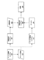
- デバイスヘテロ構造の一セットの半導体層において半導体層に対するオーミックコンタクトを含むデバイスヘテロ構造を含むデバイスであって、
前記オーミックコンタクトが、前記半導体層の一セットのコンタクト領域上に形成された一セットの高導電性半導体層を含み、
前記一セットの高導電性半導体層が、前記半導体層と前記一セットの高導電性半導体層との界面において前記半導体層と格子整合されることを特徴とするデバイス。 - 前記一セットの高導電性半導体層がIII族窒化物材料で形成される、請求項12に記載のデバイス。
- 前記一セットの高導電性半導体層がデルタドーピングされる、請求項12に記載のデバイス。
- 前記一セットの高導電性半導体層が、前記一セットのコンタクト領域からの距離に関して前記一セットの高導電性半導体層を形成する材料の少なくとも1つの元素の傾斜したモル分率を有する、請求項12に記載のデバイス。
- 前記傾斜が、前記一セットのコンタクト領域での逆キャリアの蓄積の誘起を避けるように構成される、請求項15に記載のデバイス。
Applications Claiming Priority (3)
| Application Number | Priority Date | Filing Date | Title |
|---|---|---|---|
| US201261602155P | 2012-02-23 | 2012-02-23 | |
| US61/602,155 | 2012-02-23 | ||
| PCT/US2013/027496 WO2013126828A1 (en) | 2012-02-23 | 2013-02-22 | Ohmic contact to semiconductor |
Publications (3)
| Publication Number | Publication Date |
|---|---|
| JP2015513798A JP2015513798A (ja) | 2015-05-14 |
| JP2015513798A5 JP2015513798A5 (ja) | 2016-04-07 |
| JP6186380B2 true JP6186380B2 (ja) | 2017-08-23 |
Family
ID=49001887
Family Applications (1)
| Application Number | Title | Priority Date | Filing Date |
|---|---|---|---|
| JP2014558905A Active JP6186380B2 (ja) | 2012-02-23 | 2013-02-22 | 半導体層に対するオーミックコンタクトを含むデバイスヘテロ構造を形成することを含む方法および半導体層に対するオーミックコンタクトを含むデバイスヘテロ構造を含むデバイス |
Country Status (5)
| Country | Link |
|---|---|
| US (2) | US9269788B2 (ja) |
| EP (1) | EP2817834B1 (ja) |
| JP (1) | JP6186380B2 (ja) |
| KR (2) | KR102288118B1 (ja) |
| WO (1) | WO2013126828A1 (ja) |
Families Citing this family (27)
| Publication number | Priority date | Publication date | Assignee | Title |
|---|---|---|---|---|
| KR101731056B1 (ko) * | 2010-08-13 | 2017-04-27 | 서울바이오시스 주식회사 | 오믹 전극 구조체를 갖는 반도체 발광 소자 및 그것을 제조하는 방법 |
| US9412911B2 (en) | 2013-07-09 | 2016-08-09 | The Silanna Group Pty Ltd | Optical tuning of light emitting semiconductor junctions |
| WO2015061325A1 (en) * | 2013-10-21 | 2015-04-30 | Sensor Electronic Technology, Inc. | Heterostructure including a composite semiconductor layer |
| JP6206159B2 (ja) * | 2013-12-17 | 2017-10-04 | 三菱電機株式会社 | 半導体装置の製造方法 |
| KR102427203B1 (ko) | 2014-05-27 | 2022-07-29 | 실라나 유브이 테크놀로지스 피티이 리미티드 | n-형 및 p-형 초격자를 포함하는 전자 디바이스 |
| JP6817072B2 (ja) | 2014-05-27 | 2021-01-20 | シランナ・ユー・ブイ・テクノロジーズ・プライベート・リミテッドSilanna Uv Technologies Pte Ltd | 光電子デバイス |
| US11322643B2 (en) | 2014-05-27 | 2022-05-03 | Silanna UV Technologies Pte Ltd | Optoelectronic device |
| KR102318317B1 (ko) | 2014-05-27 | 2021-10-28 | 실라나 유브이 테크놀로지스 피티이 리미티드 | 반도체 구조물과 초격자를 사용하는 진보된 전자 디바이스 구조 |
| JP6330604B2 (ja) * | 2014-09-24 | 2018-05-30 | 日亜化学工業株式会社 | 半導体発光素子 |
| CN104462290B (zh) * | 2014-11-27 | 2017-10-10 | 华为技术有限公司 | 文件系统复制方法及装置 |
| US20160169833A1 (en) * | 2014-12-11 | 2016-06-16 | International Business Machines Corporation | Biosensor based on heterojunction bipolar transistor |
| KR101641654B1 (ko) | 2015-05-13 | 2016-07-22 | 한국기계연구원 | 반도체 소자 및 반도체 소자 제조방법 |
| WO2017011474A1 (en) | 2015-07-13 | 2017-01-19 | Sensor Electronic Technology, Inc. | P-type contact to semiconductor heterostructure |
| US10236415B2 (en) | 2015-07-13 | 2019-03-19 | Sensor Electronic Technology, Inc. | P-type contact to semiconductor heterostructure |
| KR20170015645A (ko) | 2015-07-29 | 2017-02-09 | 한국기계연구원 | 트랜지스터 및 트랜지스터 제조방법 |
| DE102015122641A1 (de) * | 2015-12-22 | 2017-06-22 | Osram Opto Semiconductors Gmbh | Verfahren zum Herstellen eines optoelektronischen Bauelements und optoelektronisches Bauelement |
| WO2017145026A1 (en) | 2016-02-23 | 2017-08-31 | Silanna UV Technologies Pte Ltd | Resonant optical cavity light emitting device |
| US10418517B2 (en) | 2016-02-23 | 2019-09-17 | Silanna UV Technologies Pte Ltd | Resonant optical cavity light emitting device |
| KR102445157B1 (ko) | 2016-04-05 | 2022-09-22 | 한국재료연구원 | 2차원 전이금속 디칼코지나이드계 합금 및 그 제조방법, 2차원 전이금속 디칼코지나이드계 합금을 포함하는 트랜지스터 및 그 제조방법 |
| DE102016013540A1 (de) * | 2016-11-14 | 2018-05-17 | 3 - 5 Power Electronics GmbH | lll-V-Halbleiterdiode |
| US10177267B2 (en) * | 2017-03-03 | 2019-01-08 | Bolb Inc. | Photodetector |
| DE102017105397A1 (de) | 2017-03-14 | 2018-09-20 | Osram Opto Semiconductors Gmbh | Verfahren zur Herstellung von Leuchtdioden und Leuchtdiode |
| CN111279495B (zh) * | 2017-10-16 | 2023-06-09 | 阿卜杜拉国王科技大学 | 具有氮化硼合金接触层的iii族氮化物半导体器件及其制造方法 |
| CN109755356B (zh) * | 2017-11-07 | 2020-08-21 | 山东浪潮华光光电子股份有限公司 | 一种提升GaN基发光二极管内置欧姆接触性能的方法 |
| US10622514B1 (en) | 2018-10-15 | 2020-04-14 | Silanna UV Technologies Pte Ltd | Resonant optical cavity light emitting device |
| KR20220070127A (ko) | 2020-11-20 | 2022-05-30 | 고려대학교 산학협력단 | 나노로드 발광소자 및 그 제조 방법 |
| CN116387152B (zh) * | 2023-06-06 | 2023-12-22 | 江苏能华微电子科技发展有限公司 | 一种低损伤氮化镓肖特基二极管及其制备方法 |
Family Cites Families (25)
| Publication number | Priority date | Publication date | Assignee | Title |
|---|---|---|---|---|
| JP3502651B2 (ja) * | 1993-02-08 | 2004-03-02 | トリクイント セミコンダクター テキサス、エルピー | 電極形成法 |
| JP3216354B2 (ja) | 1993-08-11 | 2001-10-09 | ソニー株式会社 | オーミック電極およびその形成方法ならびに半導体装置 |
| US5818078A (en) | 1994-08-29 | 1998-10-06 | Fujitsu Limited | Semiconductor device having a regrowth crystal region |
| JP3571401B2 (ja) * | 1995-03-16 | 2004-09-29 | ローム株式会社 | 半導体発光素子の製法 |
| JPH11274468A (ja) | 1998-03-25 | 1999-10-08 | Sony Corp | オーミック電極およびその形成方法ならびにオーミック電極形成用積層体 |
| US6657300B2 (en) | 1998-06-05 | 2003-12-02 | Lumileds Lighting U.S., Llc | Formation of ohmic contacts in III-nitride light emitting devices |
| GB9913950D0 (en) * | 1999-06-15 | 1999-08-18 | Arima Optoelectronics Corp | Unipolar light emitting devices based on iii-nitride semiconductor superlattices |
| US6858522B1 (en) | 2000-09-28 | 2005-02-22 | Skyworks Solutions, Inc. | Electrical contact for compound semiconductor device and method for forming same |
| US6982204B2 (en) | 2002-07-16 | 2006-01-03 | Cree, Inc. | Nitride-based transistors and methods of fabrication thereof using non-etched contact recesses |
| JP4224423B2 (ja) | 2003-06-10 | 2009-02-12 | パナソニック株式会社 | 半導体装置およびその製造方法 |
| US7943949B2 (en) | 2004-09-09 | 2011-05-17 | Bridgelux, Inc. | III-nitride based on semiconductor device with low-resistance ohmic contacts |
| JP4493041B2 (ja) * | 2005-03-10 | 2010-06-30 | パナソニック株式会社 | 窒化物半導体発光素子 |
| US7399692B2 (en) * | 2005-10-03 | 2008-07-15 | International Rectifier Corporation | III-nitride semiconductor fabrication |
| JP2008091595A (ja) | 2006-10-02 | 2008-04-17 | Eudyna Devices Inc | 半導体装置およびその製造方法 |
| JP2008124262A (ja) | 2006-11-13 | 2008-05-29 | Oki Electric Ind Co Ltd | 選択再成長を用いたAlGaN/GaN−HEMTの製造方法 |
| US8878245B2 (en) | 2006-11-30 | 2014-11-04 | Cree, Inc. | Transistors and method for making ohmic contact to transistors |
| US7791101B2 (en) | 2008-03-28 | 2010-09-07 | Cree, Inc. | Indium gallium nitride-based ohmic contact layers for gallium nitride-based devices |
| KR100988126B1 (ko) | 2008-09-18 | 2010-10-18 | 고려대학교 산학협력단 | 이온주입을 통한 질화물 반도체 형성 방법 및 이를 이용하여 제조한 발광다이오드 |
| KR100999689B1 (ko) * | 2008-10-17 | 2010-12-08 | 엘지이노텍 주식회사 | 반도체 발광소자 및 그 제조방법, 이를 구비한 발광장치 |
| WO2010116699A1 (ja) | 2009-04-06 | 2010-10-14 | 住友化学株式会社 | 半導体基板、半導体基板の製造方法、半導体基板の判定方法、および電子デバイス |
| JP2010287637A (ja) * | 2009-06-10 | 2010-12-24 | Sony Corp | 半導体発光装置の製造方法 |
| CN102598207A (zh) | 2009-11-03 | 2012-07-18 | 加利福尼亚大学董事会 | 获得与非极性和半极性P-型(Al,Ga,In)N低电阻接触的技术 |
| KR101172857B1 (ko) | 2009-12-14 | 2012-08-09 | 경북대학교 산학협력단 | 인헨스먼트 노멀리 오프 질화물 반도체 소자 및 그 제조방법 |
| KR20110085680A (ko) * | 2010-01-21 | 2011-07-27 | 엘지전자 주식회사 | 질화물 반도체 소자 및 그 제조방법 |
| US8344421B2 (en) | 2010-05-11 | 2013-01-01 | Iqe Rf, Llc | Group III-nitride enhancement mode field effect devices and fabrication methods |
-
2013
- 2013-02-22 US US13/775,038 patent/US9269788B2/en active Active
- 2013-02-22 KR KR1020207007518A patent/KR102288118B1/ko active IP Right Grant
- 2013-02-22 EP EP13752529.1A patent/EP2817834B1/en active Active
- 2013-02-22 KR KR1020147026651A patent/KR102130488B1/ko active IP Right Grant
- 2013-02-22 WO PCT/US2013/027496 patent/WO2013126828A1/en active Application Filing
- 2013-02-22 JP JP2014558905A patent/JP6186380B2/ja active Active
-
2015
- 2015-12-17 US US14/973,563 patent/US9543400B2/en active Active
Also Published As
| Publication number | Publication date |
|---|---|
| US20130221406A1 (en) | 2013-08-29 |
| EP2817834B1 (en) | 2020-07-15 |
| US9543400B2 (en) | 2017-01-10 |
| KR102288118B1 (ko) | 2021-08-11 |
| US9269788B2 (en) | 2016-02-23 |
| EP2817834A1 (en) | 2014-12-31 |
| JP2015513798A (ja) | 2015-05-14 |
| EP2817834A4 (en) | 2015-10-21 |
| WO2013126828A1 (en) | 2013-08-29 |
| KR20200034801A (ko) | 2020-03-31 |
| US20160104784A1 (en) | 2016-04-14 |
| KR20140138204A (ko) | 2014-12-03 |
| KR102130488B1 (ko) | 2020-07-07 |
Similar Documents
| Publication | Publication Date | Title |
|---|---|---|
| JP6186380B2 (ja) | 半導体層に対するオーミックコンタクトを含むデバイスヘテロ構造を形成することを含む方法および半導体層に対するオーミックコンタクトを含むデバイスヘテロ構造を含むデバイス | |
| US20210028328A1 (en) | Light Extraction from Optoelectronic Device | |
| US9876140B2 (en) | Semiconductor structure with stress-reducing buffer structure | |
| US9911895B2 (en) | Semiconductor structure with inhomogeneous regions | |
| US8981403B2 (en) | Patterned substrate design for layer growth | |
| US9735315B2 (en) | Semiconductor heterostructure with stress management | |
| US10186632B2 (en) | Deep ultraviolet light emitting diode | |
| US9793367B2 (en) | Ohmic contact to semiconductor | |
| US10923619B2 (en) | Semiconductor heterostructure with at least one stress control layer | |
| US9799793B2 (en) | Semiconductor heterostructure with stress management | |
| US9923117B2 (en) | Semiconductor structure with inhomogeneous regions | |
| US20240154062A1 (en) | Multi-Period Patterned Substrate | |
| US9960321B2 (en) | Multi-layered contact to semiconductor structure | |
| US11764330B2 (en) | Optoelectronic semiconductor component having a semiconductor contact layer and method for producing the optoelectronic semiconductor component |
Legal Events
| Date | Code | Title | Description |
|---|---|---|---|
| A521 | Request for written amendment filed |
Free format text: JAPANESE INTERMEDIATE CODE: A523 Effective date: 20160210 |
|
| A621 | Written request for application examination |
Free format text: JAPANESE INTERMEDIATE CODE: A621 Effective date: 20160210 |
|
| A977 | Report on retrieval |
Free format text: JAPANESE INTERMEDIATE CODE: A971007 Effective date: 20161129 |
|
| A131 | Notification of reasons for refusal |
Free format text: JAPANESE INTERMEDIATE CODE: A131 Effective date: 20170104 |
|
| A601 | Written request for extension of time |
Free format text: JAPANESE INTERMEDIATE CODE: A601 Effective date: 20170327 |
|
| A521 | Request for written amendment filed |
Free format text: JAPANESE INTERMEDIATE CODE: A523 Effective date: 20170622 |
|
| TRDD | Decision of grant or rejection written | ||
| A01 | Written decision to grant a patent or to grant a registration (utility model) |
Free format text: JAPANESE INTERMEDIATE CODE: A01 Effective date: 20170704 |
|
| A61 | First payment of annual fees (during grant procedure) |
Free format text: JAPANESE INTERMEDIATE CODE: A61 Effective date: 20170731 |
|
| R150 | Certificate of patent or registration of utility model |
Ref document number: 6186380 Country of ref document: JP Free format text: JAPANESE INTERMEDIATE CODE: R150 |
|
| R250 | Receipt of annual fees |
Free format text: JAPANESE INTERMEDIATE CODE: R250 |
|
| R250 | Receipt of annual fees |
Free format text: JAPANESE INTERMEDIATE CODE: R250 |
|
| R250 | Receipt of annual fees |
Free format text: JAPANESE INTERMEDIATE CODE: R250 |
|
| R250 | Receipt of annual fees |
Free format text: JAPANESE INTERMEDIATE CODE: R250 |