JP6162918B1 - 高効率太陽電池の製造方法 - Google Patents
高効率太陽電池の製造方法 Download PDFInfo
- Publication number
- JP6162918B1 JP6162918B1 JP2017519714A JP2017519714A JP6162918B1 JP 6162918 B1 JP6162918 B1 JP 6162918B1 JP 2017519714 A JP2017519714 A JP 2017519714A JP 2017519714 A JP2017519714 A JP 2017519714A JP 6162918 B1 JP6162918 B1 JP 6162918B1
- Authority
- JP
- Japan
- Prior art keywords
- insulating film
- electrode
- resin
- curing
- film precursor
- Prior art date
- Legal status (The legal status is an assumption and is not a legal conclusion. Google has not performed a legal analysis and makes no representation as to the accuracy of the status listed.)
- Active
Links
- 238000004519 manufacturing process Methods 0.000 title claims abstract description 19
- 239000002243 precursor Substances 0.000 claims abstract description 63
- 238000000034 method Methods 0.000 claims abstract description 40
- 239000000758 substrate Substances 0.000 claims abstract description 40
- 239000004065 semiconductor Substances 0.000 claims abstract description 15
- 229920005989 resin Polymers 0.000 claims description 25
- 239000011347 resin Substances 0.000 claims description 25
- 229920001721 polyimide Polymers 0.000 claims description 12
- 239000004925 Acrylic resin Substances 0.000 claims description 6
- 229920000178 Acrylic resin Polymers 0.000 claims description 6
- 229910021419 crystalline silicon Inorganic materials 0.000 claims description 6
- 239000005011 phenolic resin Substances 0.000 claims description 6
- 239000004645 polyester resin Substances 0.000 claims description 6
- 229920001225 polyester resin Polymers 0.000 claims description 6
- 229920002050 silicone resin Polymers 0.000 claims description 6
- 239000003822 epoxy resin Substances 0.000 claims description 5
- 229920000647 polyepoxide Polymers 0.000 claims description 5
- 239000009719 polyimide resin Substances 0.000 claims description 4
- IMROMDMJAWUWLK-UHFFFAOYSA-N Ethenol Chemical compound OC=C IMROMDMJAWUWLK-UHFFFAOYSA-N 0.000 claims description 3
- 239000004640 Melamine resin Substances 0.000 claims description 3
- 229920000877 Melamine resin Polymers 0.000 claims description 3
- 239000004962 Polyamide-imide Substances 0.000 claims description 3
- 229920001807 Urea-formaldehyde Polymers 0.000 claims description 3
- 229920006122 polyamide resin Polymers 0.000 claims description 3
- 229920002312 polyamide-imide Polymers 0.000 claims description 3
- 229920002635 polyurethane Polymers 0.000 claims description 3
- 239000004814 polyurethane Substances 0.000 claims description 3
- 229920002451 polyvinyl alcohol Polymers 0.000 claims description 3
- YCKRFDGAMUMZLT-UHFFFAOYSA-N Fluorine atom Chemical compound [F] YCKRFDGAMUMZLT-UHFFFAOYSA-N 0.000 claims description 2
- 239000011737 fluorine Substances 0.000 claims description 2
- 229910052731 fluorine Inorganic materials 0.000 claims description 2
- 238000006243 chemical reaction Methods 0.000 abstract description 6
- 238000010438 heat treatment Methods 0.000 description 15
- 239000004642 Polyimide Substances 0.000 description 8
- 238000007650 screen-printing Methods 0.000 description 8
- 229920001187 thermosetting polymer Polymers 0.000 description 8
- 230000015572 biosynthetic process Effects 0.000 description 7
- 238000002161 passivation Methods 0.000 description 7
- 230000000052 comparative effect Effects 0.000 description 6
- 239000002904 solvent Substances 0.000 description 5
- 229910052581 Si3N4 Inorganic materials 0.000 description 4
- VYPSYNLAJGMNEJ-UHFFFAOYSA-N Silicium dioxide Chemical compound O=[Si]=O VYPSYNLAJGMNEJ-UHFFFAOYSA-N 0.000 description 4
- XUIMIQQOPSSXEZ-UHFFFAOYSA-N Silicon Chemical compound [Si] XUIMIQQOPSSXEZ-UHFFFAOYSA-N 0.000 description 4
- 239000011248 coating agent Substances 0.000 description 4
- 229910052710 silicon Inorganic materials 0.000 description 4
- 239000010703 silicon Substances 0.000 description 4
- HQVNEWCFYHHQES-UHFFFAOYSA-N silicon nitride Chemical compound N12[Si]34N5[Si]62N3[Si]51N64 HQVNEWCFYHHQES-UHFFFAOYSA-N 0.000 description 4
- 229910052814 silicon oxide Inorganic materials 0.000 description 4
- 229910052724 xenon Inorganic materials 0.000 description 4
- FHNFHKCVQCLJFQ-UHFFFAOYSA-N xenon atom Chemical compound [Xe] FHNFHKCVQCLJFQ-UHFFFAOYSA-N 0.000 description 4
- BQCADISMDOOEFD-UHFFFAOYSA-N Silver Chemical compound [Ag] BQCADISMDOOEFD-UHFFFAOYSA-N 0.000 description 3
- 239000012298 atmosphere Substances 0.000 description 3
- 238000000576 coating method Methods 0.000 description 3
- 238000009792 diffusion process Methods 0.000 description 3
- 229910052709 silver Inorganic materials 0.000 description 3
- 239000004332 silver Substances 0.000 description 3
- 239000000126 substance Substances 0.000 description 3
- RYGMFSIKBFXOCR-UHFFFAOYSA-N Copper Chemical compound [Cu] RYGMFSIKBFXOCR-UHFFFAOYSA-N 0.000 description 2
- 239000004593 Epoxy Substances 0.000 description 2
- SECXISVLQFMRJM-UHFFFAOYSA-N N-Methylpyrrolidone Chemical compound CN1CCCC1=O SECXISVLQFMRJM-UHFFFAOYSA-N 0.000 description 2
- XAGFODPZIPBFFR-UHFFFAOYSA-N aluminium Chemical compound [Al] XAGFODPZIPBFFR-UHFFFAOYSA-N 0.000 description 2
- 238000005229 chemical vapour deposition Methods 0.000 description 2
- 238000007796 conventional method Methods 0.000 description 2
- 229910052802 copper Inorganic materials 0.000 description 2
- 239000010949 copper Substances 0.000 description 2
- 238000007641 inkjet printing Methods 0.000 description 2
- 238000009413 insulation Methods 0.000 description 2
- XHXFXVLFKHQFAL-UHFFFAOYSA-N phosphoryl trichloride Chemical compound ClP(Cl)(Cl)=O XHXFXVLFKHQFAL-UHFFFAOYSA-N 0.000 description 2
- 230000007261 regionalization Effects 0.000 description 2
- 239000012808 vapor phase Substances 0.000 description 2
- OAICVXFJPJFONN-UHFFFAOYSA-N Phosphorus Chemical compound [P] OAICVXFJPJFONN-UHFFFAOYSA-N 0.000 description 1
- 206010037660 Pyrexia Diseases 0.000 description 1
- 239000000853 adhesive Substances 0.000 description 1
- 230000001070 adhesive effect Effects 0.000 description 1
- 229910052782 aluminium Inorganic materials 0.000 description 1
- 229910052787 antimony Inorganic materials 0.000 description 1
- WATWJIUSRGPENY-UHFFFAOYSA-N antimony atom Chemical compound [Sb] WATWJIUSRGPENY-UHFFFAOYSA-N 0.000 description 1
- 229910052785 arsenic Inorganic materials 0.000 description 1
- RQNWIZPPADIBDY-UHFFFAOYSA-N arsenic atom Chemical compound [As] RQNWIZPPADIBDY-UHFFFAOYSA-N 0.000 description 1
- QVGXLLKOCUKJST-UHFFFAOYSA-N atomic oxygen Chemical compound [O] QVGXLLKOCUKJST-UHFFFAOYSA-N 0.000 description 1
- 239000011230 binding agent Substances 0.000 description 1
- 239000004020 conductor Substances 0.000 description 1
- 239000013078 crystal Substances 0.000 description 1
- 238000001035 drying Methods 0.000 description 1
- 230000000694 effects Effects 0.000 description 1
- 238000010304 firing Methods 0.000 description 1
- -1 fluororesin Substances 0.000 description 1
- 239000011521 glass Substances 0.000 description 1
- 238000000608 laser ablation Methods 0.000 description 1
- 239000000463 material Substances 0.000 description 1
- 238000002156 mixing Methods 0.000 description 1
- 239000000203 mixture Substances 0.000 description 1
- 230000003287 optical effect Effects 0.000 description 1
- 230000003647 oxidation Effects 0.000 description 1
- 238000007254 oxidation reaction Methods 0.000 description 1
- 229910052760 oxygen Inorganic materials 0.000 description 1
- 239000001301 oxygen Substances 0.000 description 1
- 229910052698 phosphorus Inorganic materials 0.000 description 1
- 239000011574 phosphorus Substances 0.000 description 1
- 238000005268 plasma chemical vapour deposition Methods 0.000 description 1
- 239000004033 plastic Substances 0.000 description 1
- 229920003023 plastic Polymers 0.000 description 1
- 238000007747 plating Methods 0.000 description 1
- 239000000843 powder Substances 0.000 description 1
- 238000007639 printing Methods 0.000 description 1
- 239000002994 raw material Substances 0.000 description 1
- 238000009281 ultraviolet germicidal irradiation Methods 0.000 description 1
Images


Classifications
-
- H—ELECTRICITY
- H01—ELECTRIC ELEMENTS
- H01L—SEMICONDUCTOR DEVICES NOT COVERED BY CLASS H10
- H01L31/00—Semiconductor devices sensitive to infrared radiation, light, electromagnetic radiation of shorter wavelength or corpuscular radiation and specially adapted either for the conversion of the energy of such radiation into electrical energy or for the control of electrical energy by such radiation; Processes or apparatus specially adapted for the manufacture or treatment thereof or of parts thereof; Details thereof
- H01L31/02—Details
- H01L31/0224—Electrodes
- H01L31/022408—Electrodes for devices characterised by at least one potential jump barrier or surface barrier
- H01L31/022425—Electrodes for devices characterised by at least one potential jump barrier or surface barrier for solar cells
- H01L31/022441—Electrode arrangements specially adapted for back-contact solar cells
-
- H—ELECTRICITY
- H01—ELECTRIC ELEMENTS
- H01L—SEMICONDUCTOR DEVICES NOT COVERED BY CLASS H10
- H01L21/00—Processes or apparatus adapted for the manufacture or treatment of semiconductor or solid state devices or of parts thereof
- H01L21/02—Manufacture or treatment of semiconductor devices or of parts thereof
- H01L21/02104—Forming layers
- H01L21/02107—Forming insulating materials on a substrate
- H01L21/02296—Forming insulating materials on a substrate characterised by the treatment performed before or after the formation of the layer
- H01L21/02318—Forming insulating materials on a substrate characterised by the treatment performed before or after the formation of the layer post-treatment
- H01L21/02345—Forming insulating materials on a substrate characterised by the treatment performed before or after the formation of the layer post-treatment treatment by exposure to radiation, e.g. visible light
- H01L21/02348—Forming insulating materials on a substrate characterised by the treatment performed before or after the formation of the layer post-treatment treatment by exposure to radiation, e.g. visible light treatment by exposure to UV light
-
- H—ELECTRICITY
- H01—ELECTRIC ELEMENTS
- H01L—SEMICONDUCTOR DEVICES NOT COVERED BY CLASS H10
- H01L21/00—Processes or apparatus adapted for the manufacture or treatment of semiconductor or solid state devices or of parts thereof
- H01L21/02—Manufacture or treatment of semiconductor devices or of parts thereof
- H01L21/04—Manufacture or treatment of semiconductor devices or of parts thereof the devices having at least one potential-jump barrier or surface barrier, e.g. PN junction, depletion layer or carrier concentration layer
- H01L21/18—Manufacture or treatment of semiconductor devices or of parts thereof the devices having at least one potential-jump barrier or surface barrier, e.g. PN junction, depletion layer or carrier concentration layer the devices having semiconductor bodies comprising elements of Group IV of the Periodic System or AIIIBV compounds with or without impurities, e.g. doping materials
- H01L21/30—Treatment of semiconductor bodies using processes or apparatus not provided for in groups H01L21/20 - H01L21/26
- H01L21/31—Treatment of semiconductor bodies using processes or apparatus not provided for in groups H01L21/20 - H01L21/26 to form insulating layers thereon, e.g. for masking or by using photolithographic techniques; After treatment of these layers; Selection of materials for these layers
- H01L21/3105—After-treatment
- H01L21/31058—After-treatment of organic layers
-
- H—ELECTRICITY
- H01—ELECTRIC ELEMENTS
- H01L—SEMICONDUCTOR DEVICES NOT COVERED BY CLASS H10
- H01L21/00—Processes or apparatus adapted for the manufacture or treatment of semiconductor or solid state devices or of parts thereof
- H01L21/02—Manufacture or treatment of semiconductor devices or of parts thereof
- H01L21/04—Manufacture or treatment of semiconductor devices or of parts thereof the devices having at least one potential-jump barrier or surface barrier, e.g. PN junction, depletion layer or carrier concentration layer
- H01L21/18—Manufacture or treatment of semiconductor devices or of parts thereof the devices having at least one potential-jump barrier or surface barrier, e.g. PN junction, depletion layer or carrier concentration layer the devices having semiconductor bodies comprising elements of Group IV of the Periodic System or AIIIBV compounds with or without impurities, e.g. doping materials
- H01L21/30—Treatment of semiconductor bodies using processes or apparatus not provided for in groups H01L21/20 - H01L21/26
- H01L21/31—Treatment of semiconductor bodies using processes or apparatus not provided for in groups H01L21/20 - H01L21/26 to form insulating layers thereon, e.g. for masking or by using photolithographic techniques; After treatment of these layers; Selection of materials for these layers
- H01L21/3205—Deposition of non-insulating-, e.g. conductive- or resistive-, layers on insulating layers; After-treatment of these layers
- H01L21/321—After treatment
-
- H—ELECTRICITY
- H01—ELECTRIC ELEMENTS
- H01L—SEMICONDUCTOR DEVICES NOT COVERED BY CLASS H10
- H01L31/00—Semiconductor devices sensitive to infrared radiation, light, electromagnetic radiation of shorter wavelength or corpuscular radiation and specially adapted either for the conversion of the energy of such radiation into electrical energy or for the control of electrical energy by such radiation; Processes or apparatus specially adapted for the manufacture or treatment thereof or of parts thereof; Details thereof
- H01L31/02—Details
- H01L31/0216—Coatings
- H01L31/02161—Coatings for devices characterised by at least one potential jump barrier or surface barrier
- H01L31/02167—Coatings for devices characterised by at least one potential jump barrier or surface barrier for solar cells
-
- H—ELECTRICITY
- H01—ELECTRIC ELEMENTS
- H01L—SEMICONDUCTOR DEVICES NOT COVERED BY CLASS H10
- H01L31/00—Semiconductor devices sensitive to infrared radiation, light, electromagnetic radiation of shorter wavelength or corpuscular radiation and specially adapted either for the conversion of the energy of such radiation into electrical energy or for the control of electrical energy by such radiation; Processes or apparatus specially adapted for the manufacture or treatment thereof or of parts thereof; Details thereof
- H01L31/02—Details
- H01L31/0224—Electrodes
- H01L31/022408—Electrodes for devices characterised by at least one potential jump barrier or surface barrier
- H01L31/022425—Electrodes for devices characterised by at least one potential jump barrier or surface barrier for solar cells
- H01L31/022441—Electrode arrangements specially adapted for back-contact solar cells
- H01L31/022458—Electrode arrangements specially adapted for back-contact solar cells for emitter wrap-through [EWT] type solar cells, e.g. interdigitated emitter-base back-contacts
-
- H—ELECTRICITY
- H01—ELECTRIC ELEMENTS
- H01L—SEMICONDUCTOR DEVICES NOT COVERED BY CLASS H10
- H01L31/00—Semiconductor devices sensitive to infrared radiation, light, electromagnetic radiation of shorter wavelength or corpuscular radiation and specially adapted either for the conversion of the energy of such radiation into electrical energy or for the control of electrical energy by such radiation; Processes or apparatus specially adapted for the manufacture or treatment thereof or of parts thereof; Details thereof
- H01L31/0248—Semiconductor devices sensitive to infrared radiation, light, electromagnetic radiation of shorter wavelength or corpuscular radiation and specially adapted either for the conversion of the energy of such radiation into electrical energy or for the control of electrical energy by such radiation; Processes or apparatus specially adapted for the manufacture or treatment thereof or of parts thereof; Details thereof characterised by their semiconductor bodies
- H01L31/0256—Semiconductor devices sensitive to infrared radiation, light, electromagnetic radiation of shorter wavelength or corpuscular radiation and specially adapted either for the conversion of the energy of such radiation into electrical energy or for the control of electrical energy by such radiation; Processes or apparatus specially adapted for the manufacture or treatment thereof or of parts thereof; Details thereof characterised by their semiconductor bodies characterised by the material
- H01L31/0264—Inorganic materials
- H01L31/028—Inorganic materials including, apart from doping material or other impurities, only elements of Group IV of the Periodic System
-
- H—ELECTRICITY
- H01—ELECTRIC ELEMENTS
- H01L—SEMICONDUCTOR DEVICES NOT COVERED BY CLASS H10
- H01L31/00—Semiconductor devices sensitive to infrared radiation, light, electromagnetic radiation of shorter wavelength or corpuscular radiation and specially adapted either for the conversion of the energy of such radiation into electrical energy or for the control of electrical energy by such radiation; Processes or apparatus specially adapted for the manufacture or treatment thereof or of parts thereof; Details thereof
- H01L31/0248—Semiconductor devices sensitive to infrared radiation, light, electromagnetic radiation of shorter wavelength or corpuscular radiation and specially adapted either for the conversion of the energy of such radiation into electrical energy or for the control of electrical energy by such radiation; Processes or apparatus specially adapted for the manufacture or treatment thereof or of parts thereof; Details thereof characterised by their semiconductor bodies
- H01L31/036—Semiconductor devices sensitive to infrared radiation, light, electromagnetic radiation of shorter wavelength or corpuscular radiation and specially adapted either for the conversion of the energy of such radiation into electrical energy or for the control of electrical energy by such radiation; Processes or apparatus specially adapted for the manufacture or treatment thereof or of parts thereof; Details thereof characterised by their semiconductor bodies characterised by their crystalline structure or particular orientation of the crystalline planes
-
- H—ELECTRICITY
- H01—ELECTRIC ELEMENTS
- H01L—SEMICONDUCTOR DEVICES NOT COVERED BY CLASS H10
- H01L31/00—Semiconductor devices sensitive to infrared radiation, light, electromagnetic radiation of shorter wavelength or corpuscular radiation and specially adapted either for the conversion of the energy of such radiation into electrical energy or for the control of electrical energy by such radiation; Processes or apparatus specially adapted for the manufacture or treatment thereof or of parts thereof; Details thereof
- H01L31/04—Semiconductor devices sensitive to infrared radiation, light, electromagnetic radiation of shorter wavelength or corpuscular radiation and specially adapted either for the conversion of the energy of such radiation into electrical energy or for the control of electrical energy by such radiation; Processes or apparatus specially adapted for the manufacture or treatment thereof or of parts thereof; Details thereof adapted as photovoltaic [PV] conversion devices
- H01L31/06—Semiconductor devices sensitive to infrared radiation, light, electromagnetic radiation of shorter wavelength or corpuscular radiation and specially adapted either for the conversion of the energy of such radiation into electrical energy or for the control of electrical energy by such radiation; Processes or apparatus specially adapted for the manufacture or treatment thereof or of parts thereof; Details thereof adapted as photovoltaic [PV] conversion devices characterised by at least one potential-jump barrier or surface barrier
- H01L31/068—Semiconductor devices sensitive to infrared radiation, light, electromagnetic radiation of shorter wavelength or corpuscular radiation and specially adapted either for the conversion of the energy of such radiation into electrical energy or for the control of electrical energy by such radiation; Processes or apparatus specially adapted for the manufacture or treatment thereof or of parts thereof; Details thereof adapted as photovoltaic [PV] conversion devices characterised by at least one potential-jump barrier or surface barrier the potential barriers being only of the PN homojunction type, e.g. bulk silicon PN homojunction solar cells or thin film polycrystalline silicon PN homojunction solar cells
- H01L31/0682—Semiconductor devices sensitive to infrared radiation, light, electromagnetic radiation of shorter wavelength or corpuscular radiation and specially adapted either for the conversion of the energy of such radiation into electrical energy or for the control of electrical energy by such radiation; Processes or apparatus specially adapted for the manufacture or treatment thereof or of parts thereof; Details thereof adapted as photovoltaic [PV] conversion devices characterised by at least one potential-jump barrier or surface barrier the potential barriers being only of the PN homojunction type, e.g. bulk silicon PN homojunction solar cells or thin film polycrystalline silicon PN homojunction solar cells back-junction, i.e. rearside emitter, solar cells, e.g. interdigitated base-emitter regions back-junction cells
-
- H—ELECTRICITY
- H01—ELECTRIC ELEMENTS
- H01L—SEMICONDUCTOR DEVICES NOT COVERED BY CLASS H10
- H01L31/00—Semiconductor devices sensitive to infrared radiation, light, electromagnetic radiation of shorter wavelength or corpuscular radiation and specially adapted either for the conversion of the energy of such radiation into electrical energy or for the control of electrical energy by such radiation; Processes or apparatus specially adapted for the manufacture or treatment thereof or of parts thereof; Details thereof
- H01L31/18—Processes or apparatus specially adapted for the manufacture or treatment of these devices or of parts thereof
- H01L31/186—Particular post-treatment for the devices, e.g. annealing, impurity gettering, short-circuit elimination, recrystallisation
- H01L31/1864—Annealing
-
- H—ELECTRICITY
- H01—ELECTRIC ELEMENTS
- H01L—SEMICONDUCTOR DEVICES NOT COVERED BY CLASS H10
- H01L31/00—Semiconductor devices sensitive to infrared radiation, light, electromagnetic radiation of shorter wavelength or corpuscular radiation and specially adapted either for the conversion of the energy of such radiation into electrical energy or for the control of electrical energy by such radiation; Processes or apparatus specially adapted for the manufacture or treatment thereof or of parts thereof; Details thereof
- H01L31/18—Processes or apparatus specially adapted for the manufacture or treatment of these devices or of parts thereof
- H01L31/186—Particular post-treatment for the devices, e.g. annealing, impurity gettering, short-circuit elimination, recrystallisation
- H01L31/1868—Passivation
-
- Y—GENERAL TAGGING OF NEW TECHNOLOGICAL DEVELOPMENTS; GENERAL TAGGING OF CROSS-SECTIONAL TECHNOLOGIES SPANNING OVER SEVERAL SECTIONS OF THE IPC; TECHNICAL SUBJECTS COVERED BY FORMER USPC CROSS-REFERENCE ART COLLECTIONS [XRACs] AND DIGESTS
- Y02—TECHNOLOGIES OR APPLICATIONS FOR MITIGATION OR ADAPTATION AGAINST CLIMATE CHANGE
- Y02E—REDUCTION OF GREENHOUSE GAS [GHG] EMISSIONS, RELATED TO ENERGY GENERATION, TRANSMISSION OR DISTRIBUTION
- Y02E10/00—Energy generation through renewable energy sources
- Y02E10/50—Photovoltaic [PV] energy
- Y02E10/547—Monocrystalline silicon PV cells
-
- Y—GENERAL TAGGING OF NEW TECHNOLOGICAL DEVELOPMENTS; GENERAL TAGGING OF CROSS-SECTIONAL TECHNOLOGIES SPANNING OVER SEVERAL SECTIONS OF THE IPC; TECHNICAL SUBJECTS COVERED BY FORMER USPC CROSS-REFERENCE ART COLLECTIONS [XRACs] AND DIGESTS
- Y02—TECHNOLOGIES OR APPLICATIONS FOR MITIGATION OR ADAPTATION AGAINST CLIMATE CHANGE
- Y02P—CLIMATE CHANGE MITIGATION TECHNOLOGIES IN THE PRODUCTION OR PROCESSING OF GOODS
- Y02P70/00—Climate change mitigation technologies in the production process for final industrial or consumer products
- Y02P70/50—Manufacturing or production processes characterised by the final manufactured product
Abstract
Description
半導体基板の第1主表面に、第1電極を形成する工程と、
前記第1電極の少なくとも一部を覆うように、絶縁膜前駆体を塗布する工程と、
前記絶縁膜前駆体を仮硬化させる工程と、
少なくとも前記絶縁膜前駆体上に、導電性ペーストを前記第1電極と電気的に絶縁するように塗布する工程と、
前記導電性ペーストを硬化させて第2電極とする工程と、
前記絶縁膜前駆体を本硬化させて絶縁膜とする工程と、
を有し、
前記導電性ペーストを前記第1電極と電気的に絶縁するように塗布する工程は、前記絶縁膜前駆体を仮硬化させる工程後に行われ、
前記導電性ペーストを硬化させて第2電極とする工程の少なくとも一部と前記絶縁膜前駆体を本硬化させて絶縁膜とする工程の少なくとも一部が同時に行われることを特徴とする太陽電池の製造方法を提供する。
半導体基板の第1主表面に、第1電極を形成する工程と、
前記第1電極の少なくとも一部を覆うように、絶縁膜前駆体を塗布する工程と、
前記絶縁膜前駆体を仮硬化させる工程と、
少なくとも前記絶縁膜前駆体上に、導電性ペーストを前記第1電極と電気的に絶縁するように塗布する工程と、
前記導電性ペーストを硬化させて第2電極とする工程と、
前記絶縁膜前駆体を本硬化させて絶縁膜とする工程と、
を有し、
前記導電性ペーストを前記第1電極と電気的に絶縁するように塗布する工程は、前記絶縁膜前駆体を仮硬化させる工程後に行われ、
前記導電性ペーストを硬化させて第2電極とする工程の少なくとも一部と前記絶縁膜前駆体を本硬化させて絶縁膜とする工程の少なくとも一部が同時に行われることを特徴とする太陽電池の製造方法が、上記課題を解決できることを見出し、本発明を完成させた。
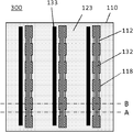
本発明の方法を用いて、図1、2に示す太陽電池の作製を行った。
実施例1と同様の基板を使用し、同様の太陽電池製造工程によりエミッタ電極とベース電極の形成までを行った。
実施例1と同様の基板を使用し、同様の太陽電池製造工程によりエミッタ電極とベース電極の形成までを行った。
実施例1と同様の基板を使用し、同様の太陽電池製造工程によりエミッタ電極とベース電極の形成までを行った。

Claims (5)
- 半導体基板の第1主表面に、第1電極を形成する工程と、
前記第1電極の少なくとも一部を覆うように、絶縁膜前駆体を塗布する工程と、
前記絶縁膜前駆体を仮硬化させる工程と、
少なくとも前記絶縁膜前駆体上に、導電性ペーストを前記第1電極と電気的に絶縁するように塗布する工程と、
前記導電性ペーストを硬化させて第2電極とする工程と、
前記絶縁膜前駆体を本硬化させて絶縁膜とする工程と、
を有し、
前記導電性ペーストを前記第1電極と電気的に絶縁するように塗布する工程は、前記絶縁膜前駆体を仮硬化させる工程後に行われ、
前記導電性ペーストを硬化させて第2電極とする工程の少なくとも一部と前記絶縁膜前駆体を本硬化させて絶縁膜とする工程の少なくとも一部が同時に行われることを特徴とする太陽電池の製造方法。 - 前記導電性ペーストを硬化させて第2電極とする工程全体が、前記絶縁膜前駆体を本硬化させて絶縁膜とする工程全体と同時に行われることを特徴とする請求項1に記載の太陽電池の製造方法。
- 前記絶縁膜を、シリコーン樹脂、ポリアミド樹脂、ポリイミド樹脂、ポリアミドイミド樹脂、フッ素樹脂、フェノール樹脂、メラミン樹脂、ユリア樹脂、ポリウレタン、エポキシ樹脂、アクリル樹脂、ポリエステル樹脂及びポバール樹脂から選択される1種類以上の樹脂を含有するものとすることを特徴とする請求項1又は請求項2に記載の太陽電池の製造方法。
- 前記導電性ペーストを、エポキシ樹脂、アクリル樹脂、ポリエステル樹脂、フェノール樹脂及びシリコーン樹脂から選択される1種類以上の樹脂を含有するものとすることを特徴とする請求項1から請求項3のいずれか1項に記載の太陽電池の製造方法。
- 前記半導体基板を、結晶シリコン基板とすることを特徴とする請求項1から請求項4のいずれか1項に記載の太陽電池の製造方法。
Applications Claiming Priority (1)
| Application Number | Priority Date | Filing Date | Title |
|---|---|---|---|
| PCT/JP2016/004822 WO2018083721A1 (ja) | 2016-11-07 | 2016-11-07 | 高効率太陽電池の製造方法 |
Publications (2)
| Publication Number | Publication Date |
|---|---|
| JP6162918B1 true JP6162918B1 (ja) | 2017-07-12 |
| JPWO2018083721A1 JPWO2018083721A1 (ja) | 2018-11-01 |
Family
ID=59308950
Family Applications (1)
| Application Number | Title | Priority Date | Filing Date |
|---|---|---|---|
| JP2017519714A Active JP6162918B1 (ja) | 2016-11-07 | 2016-11-07 | 高効率太陽電池の製造方法 |
Country Status (7)
| Country | Link |
|---|---|
| US (1) | US10236397B2 (ja) |
| EP (1) | EP3343643B1 (ja) |
| JP (1) | JP6162918B1 (ja) |
| KR (1) | KR102556599B1 (ja) |
| CN (1) | CN110050352B (ja) |
| TW (1) | TWI635623B (ja) |
| WO (1) | WO2018083721A1 (ja) |
Families Citing this family (1)
| Publication number | Priority date | Publication date | Assignee | Title |
|---|---|---|---|---|
| CN110073499B (zh) * | 2016-11-15 | 2024-04-05 | 信越化学工业株式会社 | 高效率太阳能电池及高效率太阳能电池的制造方法 |
Citations (7)
| Publication number | Priority date | Publication date | Assignee | Title |
|---|---|---|---|---|
| JP2001345470A (ja) * | 2000-06-01 | 2001-12-14 | Canon Inc | 光起電力素子の製造方法 |
| JP2008306129A (ja) * | 2007-06-11 | 2008-12-18 | Clean Venture 21 Corp | 光電変換装置の製造方法 |
| JP2009218490A (ja) * | 2008-03-12 | 2009-09-24 | Citizen Holdings Co Ltd | 太陽電池装置の製造方法 |
| JP2009253096A (ja) * | 2008-04-08 | 2009-10-29 | Sharp Corp | 太陽電池セルの製造方法および太陽電池モジュールの製造方法ならびに太陽電池モジュール |
| JP2014045124A (ja) * | 2012-08-28 | 2014-03-13 | Sharp Corp | 太陽電池およびその製造方法、並びに太陽電池モジュールおよびその製造方法 |
| JP2014120554A (ja) * | 2012-12-14 | 2014-06-30 | Sharp Corp | 太陽電池及びその製造方法 |
| WO2016125430A1 (ja) * | 2015-02-05 | 2016-08-11 | 信越化学工業株式会社 | 裏面接合型太陽電池 |
Family Cites Families (12)
| Publication number | Priority date | Publication date | Assignee | Title |
|---|---|---|---|---|
| JP2002057423A (ja) * | 2000-08-07 | 2002-02-22 | Matsushita Electric Ind Co Ltd | 導電性ペーストを用いた回路基板とその製造方法 |
| EP2068369A1 (en) * | 2007-12-03 | 2009-06-10 | Interuniversitair Microelektronica Centrum (IMEC) | Photovoltaic cells having metal wrap through and improved passivation |
| US8158504B2 (en) * | 2008-05-30 | 2012-04-17 | E. I. Du Pont De Nemours And Company | Conductive compositions and processes for use in the manufacture of semiconductor devices—organic medium components |
| WO2011033826A1 (ja) * | 2009-09-18 | 2011-03-24 | 信越化学工業株式会社 | 太陽電池、その製造方法及び太陽電池モジュール |
| JP2012069594A (ja) | 2010-09-21 | 2012-04-05 | Pi R & D Co Ltd | 太陽電池内の絶縁膜形成用ポリイミド樹脂組成物及びそれを用いた太陽電池内の絶縁膜形成方法 |
| US9281435B2 (en) * | 2011-05-27 | 2016-03-08 | Csi Cells Co., Ltd | Light to current converter devices and methods of manufacturing the same |
| WO2013125430A1 (ja) | 2012-02-23 | 2013-08-29 | 永田精機株式会社 | 穿刺針、その製造方法およびその製造装置 |
| KR101628312B1 (ko) * | 2013-10-31 | 2016-06-09 | 재단법인대구경북과학기술원 | CZTSSe계 박막 태양전지의 제조방법 및 이에 의해 제조된 CZTSSe계 박막 태양전지 |
| US10249775B2 (en) | 2014-06-11 | 2019-04-02 | Shin-Etsu Chemical Co., Ltd. | Solar cell and method for producing solar cell |
| JP6199839B2 (ja) | 2014-09-30 | 2017-09-20 | 信越化学工業株式会社 | 太陽電池及びその製造方法 |
| JP2016219452A (ja) * | 2015-05-14 | 2016-12-22 | 富士通株式会社 | 多層基板及び多層基板の製造方法 |
| EP3333901B1 (en) | 2016-10-05 | 2020-12-30 | Shin-Etsu Chemical Co., Ltd. | Method for manufacturing a high photoelectric conversion efficiency solar cell |
-
2016
- 2016-11-07 CN CN201680090581.XA patent/CN110050352B/zh active Active
- 2016-11-07 KR KR1020197012862A patent/KR102556599B1/ko active IP Right Grant
- 2016-11-07 US US15/740,160 patent/US10236397B2/en active Active
- 2016-11-07 WO PCT/JP2016/004822 patent/WO2018083721A1/ja active Application Filing
- 2016-11-07 JP JP2017519714A patent/JP6162918B1/ja active Active
- 2016-11-07 EP EP16886807.3A patent/EP3343643B1/en active Active
-
2017
- 2017-03-07 TW TW106107412A patent/TWI635623B/zh active
Patent Citations (7)
| Publication number | Priority date | Publication date | Assignee | Title |
|---|---|---|---|---|
| JP2001345470A (ja) * | 2000-06-01 | 2001-12-14 | Canon Inc | 光起電力素子の製造方法 |
| JP2008306129A (ja) * | 2007-06-11 | 2008-12-18 | Clean Venture 21 Corp | 光電変換装置の製造方法 |
| JP2009218490A (ja) * | 2008-03-12 | 2009-09-24 | Citizen Holdings Co Ltd | 太陽電池装置の製造方法 |
| JP2009253096A (ja) * | 2008-04-08 | 2009-10-29 | Sharp Corp | 太陽電池セルの製造方法および太陽電池モジュールの製造方法ならびに太陽電池モジュール |
| JP2014045124A (ja) * | 2012-08-28 | 2014-03-13 | Sharp Corp | 太陽電池およびその製造方法、並びに太陽電池モジュールおよびその製造方法 |
| JP2014120554A (ja) * | 2012-12-14 | 2014-06-30 | Sharp Corp | 太陽電池及びその製造方法 |
| WO2016125430A1 (ja) * | 2015-02-05 | 2016-08-11 | 信越化学工業株式会社 | 裏面接合型太陽電池 |
Also Published As
| Publication number | Publication date |
|---|---|
| EP3343643B1 (en) | 2021-08-04 |
| TWI635623B (zh) | 2018-09-11 |
| WO2018083721A1 (ja) | 2018-05-11 |
| KR20190076975A (ko) | 2019-07-02 |
| KR102556599B1 (ko) | 2023-07-17 |
| US10236397B2 (en) | 2019-03-19 |
| US20180315869A1 (en) | 2018-11-01 |
| CN110050352B (zh) | 2022-04-29 |
| EP3343643A4 (en) | 2019-01-23 |
| TW201818567A (zh) | 2018-05-16 |
| JPWO2018083721A1 (ja) | 2018-11-01 |
| CN110050352A (zh) | 2019-07-23 |
| EP3343643A1 (en) | 2018-07-04 |
Similar Documents
| Publication | Publication Date | Title |
|---|---|---|
| JP6199839B2 (ja) | 太陽電池及びその製造方法 | |
| US10249775B2 (en) | Solar cell and method for producing solar cell | |
| EP2184787A1 (en) | Rear surface bonding type solar cell, rear surface bonding type solar cell having wiring board, solar cell string and soar cell module | |
| WO2009125628A1 (ja) | 太陽電池セルの製造方法および太陽電池モジュールの製造方法ならびに太陽電池モジュール | |
| JP5318478B2 (ja) | 太陽電池の電極形成方法、これを利用した太陽電池の製造方法 | |
| JP6162918B1 (ja) | 高効率太陽電池の製造方法 | |
| CN109041583B (zh) | 太阳能电池元件以及太阳能电池模块 | |
| JP6405285B2 (ja) | 太陽電池の製造方法 | |
| JP6532518B2 (ja) | 高効率太陽電池の製造方法 | |
| KR20040017183A (ko) | 효율이 개선된 태양전지 및 메탈입자를 이용한 그의제조방법 | |
| JP6875252B2 (ja) | ポリイミドペーストの乾燥方法及び高光電変換効率太陽電池の製造方法 | |
| JP2016530727A (ja) | 太陽電池の製造方法 | |
| WO2018092172A1 (ja) | 高効率太陽電池及び高効率太陽電池の製造方法 | |
| CN113363346A (zh) | 背接触型太阳能电池单元的制造方法 |
Legal Events
| Date | Code | Title | Description |
|---|---|---|---|
| A621 | Written request for application examination |
Free format text: JAPANESE INTERMEDIATE CODE: A621 Effective date: 20170428 |
|
| A871 | Explanation of circumstances concerning accelerated examination |
Free format text: JAPANESE INTERMEDIATE CODE: A871 Effective date: 20170428 |
|
| A975 | Report on accelerated examination |
Free format text: JAPANESE INTERMEDIATE CODE: A971005 Effective date: 20170530 |
|
| TRDD | Decision of grant or rejection written | ||
| A01 | Written decision to grant a patent or to grant a registration (utility model) |
Free format text: JAPANESE INTERMEDIATE CODE: A01 Effective date: 20170606 |
|
| A61 | First payment of annual fees (during grant procedure) |
Free format text: JAPANESE INTERMEDIATE CODE: A61 Effective date: 20170615 |
|
| R150 | Certificate of patent or registration of utility model |
Ref document number: 6162918 Country of ref document: JP Free format text: JAPANESE INTERMEDIATE CODE: R150 |