JP6154060B2 - 混載メモリタイプハイブリッドキャッシュ - Google Patents
混載メモリタイプハイブリッドキャッシュ Download PDFInfo
- Publication number
- JP6154060B2 JP6154060B2 JP2016502013A JP2016502013A JP6154060B2 JP 6154060 B2 JP6154060 B2 JP 6154060B2 JP 2016502013 A JP2016502013 A JP 2016502013A JP 2016502013 A JP2016502013 A JP 2016502013A JP 6154060 B2 JP6154060 B2 JP 6154060B2
- Authority
- JP
- Japan
- Prior art keywords
- memory
- cache
- type
- cache line
- cached information
- Prior art date
- Legal status (The legal status is an assumption and is not a legal conclusion. Google has not performed a legal analysis and makes no representation as to the accuracy of the status listed.)
- Expired - Fee Related
Links
Images


Classifications
-
- G—PHYSICS
- G06—COMPUTING; CALCULATING OR COUNTING
- G06F—ELECTRIC DIGITAL DATA PROCESSING
- G06F12/00—Accessing, addressing or allocating within memory systems or architectures
- G06F12/02—Addressing or allocation; Relocation
- G06F12/08—Addressing or allocation; Relocation in hierarchically structured memory systems, e.g. virtual memory systems
- G06F12/0802—Addressing of a memory level in which the access to the desired data or data block requires associative addressing means, e.g. caches
- G06F12/0844—Multiple simultaneous or quasi-simultaneous cache accessing
- G06F12/0846—Cache with multiple tag or data arrays being simultaneously accessible
- G06F12/0851—Cache with interleaved addressing
-
- G—PHYSICS
- G06—COMPUTING; CALCULATING OR COUNTING
- G06F—ELECTRIC DIGITAL DATA PROCESSING
- G06F12/00—Accessing, addressing or allocating within memory systems or architectures
- G06F12/02—Addressing or allocation; Relocation
- G06F12/08—Addressing or allocation; Relocation in hierarchically structured memory systems, e.g. virtual memory systems
- G06F12/0802—Addressing of a memory level in which the access to the desired data or data block requires associative addressing means, e.g. caches
- G06F12/0844—Multiple simultaneous or quasi-simultaneous cache accessing
- G06F12/0846—Cache with multiple tag or data arrays being simultaneously accessible
-
- G—PHYSICS
- G06—COMPUTING; CALCULATING OR COUNTING
- G06F—ELECTRIC DIGITAL DATA PROCESSING
- G06F12/00—Accessing, addressing or allocating within memory systems or architectures
- G06F12/02—Addressing or allocation; Relocation
- G06F12/08—Addressing or allocation; Relocation in hierarchically structured memory systems, e.g. virtual memory systems
- G06F12/0802—Addressing of a memory level in which the access to the desired data or data block requires associative addressing means, e.g. caches
- G06F12/0893—Caches characterised by their organisation or structure
-
- G—PHYSICS
- G06—COMPUTING; CALCULATING OR COUNTING
- G06F—ELECTRIC DIGITAL DATA PROCESSING
- G06F12/00—Accessing, addressing or allocating within memory systems or architectures
- G06F12/02—Addressing or allocation; Relocation
- G06F12/08—Addressing or allocation; Relocation in hierarchically structured memory systems, e.g. virtual memory systems
- G06F12/10—Address translation
- G06F12/1027—Address translation using associative or pseudo-associative address translation means, e.g. translation look-aside buffer [TLB]
- G06F12/1045—Address translation using associative or pseudo-associative address translation means, e.g. translation look-aside buffer [TLB] associated with a data cache
-
- G—PHYSICS
- G11—INFORMATION STORAGE
- G11C—STATIC STORES
- G11C11/00—Digital stores characterised by the use of particular electric or magnetic storage elements; Storage elements therefor
- G11C11/005—Digital stores characterised by the use of particular electric or magnetic storage elements; Storage elements therefor comprising combined but independently operative RAM-ROM, RAM-PROM, RAM-EPROM cells
-
- G—PHYSICS
- G11—INFORMATION STORAGE
- G11C—STATIC STORES
- G11C11/00—Digital stores characterised by the use of particular electric or magnetic storage elements; Storage elements therefor
- G11C11/02—Digital stores characterised by the use of particular electric or magnetic storage elements; Storage elements therefor using magnetic elements
- G11C11/16—Digital stores characterised by the use of particular electric or magnetic storage elements; Storage elements therefor using magnetic elements using elements in which the storage effect is based on magnetic spin effect
- G11C11/165—Auxiliary circuits
- G11C11/1659—Cell access
-
- G—PHYSICS
- G11—INFORMATION STORAGE
- G11C—STATIC STORES
- G11C13/00—Digital stores characterised by the use of storage elements not covered by groups G11C11/00, G11C23/00, or G11C25/00
- G11C13/0002—Digital stores characterised by the use of storage elements not covered by groups G11C11/00, G11C23/00, or G11C25/00 using resistive RAM [RRAM] elements
- G11C13/0021—Auxiliary circuits
- G11C13/004—Reading or sensing circuits or methods
-
- G—PHYSICS
- G11—INFORMATION STORAGE
- G11C—STATIC STORES
- G11C13/00—Digital stores characterised by the use of storage elements not covered by groups G11C11/00, G11C23/00, or G11C25/00
- G11C13/0002—Digital stores characterised by the use of storage elements not covered by groups G11C11/00, G11C23/00, or G11C25/00 using resistive RAM [RRAM] elements
- G11C13/0021—Auxiliary circuits
- G11C13/0069—Writing or programming circuits or methods
-
- G—PHYSICS
- G11—INFORMATION STORAGE
- G11C—STATIC STORES
- G11C14/00—Digital stores characterised by arrangements of cells having volatile and non-volatile storage properties for back-up when the power is down
- G11C14/0054—Digital stores characterised by arrangements of cells having volatile and non-volatile storage properties for back-up when the power is down in which the volatile element is a SRAM cell
- G11C14/0081—Digital stores characterised by arrangements of cells having volatile and non-volatile storage properties for back-up when the power is down in which the volatile element is a SRAM cell and the nonvolatile element is a magnetic RAM [MRAM] element or ferromagnetic cell
-
- G—PHYSICS
- G06—COMPUTING; CALCULATING OR COUNTING
- G06F—ELECTRIC DIGITAL DATA PROCESSING
- G06F2212/00—Indexing scheme relating to accessing, addressing or allocation within memory systems or architectures
- G06F2212/10—Providing a specific technical effect
- G06F2212/1028—Power efficiency
-
- G—PHYSICS
- G06—COMPUTING; CALCULATING OR COUNTING
- G06F—ELECTRIC DIGITAL DATA PROCESSING
- G06F2212/00—Indexing scheme relating to accessing, addressing or allocation within memory systems or architectures
- G06F2212/20—Employing a main memory using a specific memory technology
- G06F2212/202—Non-volatile memory
- G06F2212/2024—Rewritable memory not requiring erasing, e.g. resistive or ferroelectric RAM
-
- G—PHYSICS
- G06—COMPUTING; CALCULATING OR COUNTING
- G06F—ELECTRIC DIGITAL DATA PROCESSING
- G06F2212/00—Indexing scheme relating to accessing, addressing or allocation within memory systems or architectures
- G06F2212/20—Employing a main memory using a specific memory technology
- G06F2212/205—Hybrid memory, e.g. using both volatile and non-volatile memory
-
- G—PHYSICS
- G06—COMPUTING; CALCULATING OR COUNTING
- G06F—ELECTRIC DIGITAL DATA PROCESSING
- G06F2212/00—Indexing scheme relating to accessing, addressing or allocation within memory systems or architectures
- G06F2212/22—Employing cache memory using specific memory technology
- G06F2212/225—Hybrid cache memory, e.g. having both volatile and non-volatile portions
-
- G—PHYSICS
- G11—INFORMATION STORAGE
- G11C—STATIC STORES
- G11C2207/00—Indexing scheme relating to arrangements for writing information into, or reading information out from, a digital store
- G11C2207/22—Control and timing of internal memory operations
- G11C2207/2245—Memory devices with an internal cache buffer
-
- Y—GENERAL TAGGING OF NEW TECHNOLOGICAL DEVELOPMENTS; GENERAL TAGGING OF CROSS-SECTIONAL TECHNOLOGIES SPANNING OVER SEVERAL SECTIONS OF THE IPC; TECHNICAL SUBJECTS COVERED BY FORMER USPC CROSS-REFERENCE ART COLLECTIONS [XRACs] AND DIGESTS
- Y02—TECHNOLOGIES OR APPLICATIONS FOR MITIGATION OR ADAPTATION AGAINST CLIMATE CHANGE
- Y02D—CLIMATE CHANGE MITIGATION TECHNOLOGIES IN INFORMATION AND COMMUNICATION TECHNOLOGIES [ICT], I.E. INFORMATION AND COMMUNICATION TECHNOLOGIES AIMING AT THE REDUCTION OF THEIR OWN ENERGY USE
- Y02D10/00—Energy efficient computing, e.g. low power processors, power management or thermal management
Landscapes
- Engineering & Computer Science (AREA)
- Theoretical Computer Science (AREA)
- Physics & Mathematics (AREA)
- General Engineering & Computer Science (AREA)
- General Physics & Mathematics (AREA)
- Computer Hardware Design (AREA)
- Hall/Mr Elements (AREA)
- Mram Or Spin Memory Techniques (AREA)
- Memory System Of A Hierarchy Structure (AREA)
Description
102 磁気トンネル接合
104 アクセストランジスタ
106、214 固定層
110、218 自由層
112、318 ビット線
114 トンネルバリア層
116 ゲート
118、316 ワード線
200 磁気ランダムアクセスメモリ
212、226 ビットセル
216 トンネル層
220 電流源
222、224 読取り選択トランジスタ
226 ワード線選択トランジスタ
240 基準回路
260 データ回路
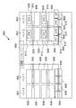
300 メモリマクロ
302 ローカルデータ経路
304 グローバルデータ経路
306 セルアレイ
308 デコーダ
310 グローバル制御ユニット
312 D IN
314 D OUT
320 単位セル
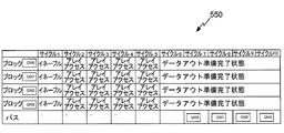
400 SRAMキャッシュ
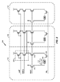
404、604、806 キャッシュインターフェース
406、606、808 SRAMマクロ
408、608、810 クアッドワード
600、800 ハイブリッドSRAM-MRAMキャッシュ
607、809 MRAMマクロ
1100 ワイヤレス通信システム
1120、1130、1150 遠隔ユニット
1140 ベースステーション
1200 設計ワークステーション
1203 駆動装置
1204 記憶媒体
Claims (17)
- 第1のタイプのメモリと、
第2のタイプのメモリと、
前記第1のタイプのメモリおよび前記第2のタイプのメモリを含む第1のメモリバンクと、
前記第1のメモリバンク内の前記第1のタイプのメモリにおける第1のメモリロケーションおよび前記第2のタイプのメモリにおける第2のメモリロケーションを含む第1のキャッシュラインであって、キャッシュアクセス動作において、前記第1のメモリバンク内の前記第2のメモリロケーションにアクセスする前に前記第1のメモリロケーションにアクセスするように構成された、第1のキャッシュラインと、
前記第1のタイプのメモリにおける第3のメモリロケーションおよび前記第2のタイプのメモリにおける第4のメモリロケーションを含む第2のキャッシュラインであって、キャッシュアクセス動作において、前記第2のメモリロケーションにアクセスする前に前記第3のメモリロケーションにアクセスするように構成された、第2のキャッシュラインと
を含むハイブリッドキャッシュ装置。 - 前記第1のメモリロケーションが、前記第1のキャッシュラインの第1のワードロケーションを含む請求項1に記載のハイブリッドキャッシュ装置。
- キャッシュされた情報のクリティカルなワードを前記第1のメモリロケーションに記憶するように構成された請求項1に記載のハイブリッドキャッシュ装置。
- 前記第2のタイプのメモリが抵抗メモリを含む請求項1に記載のハイブリッドキャッシュ装置。
- 前記第1のタイプのメモリが静的ランダムアクセスメモリ(SRAM)を含み、前記第2のタイプのメモリが磁気ランダムアクセスメモリ(MRAM)を含む請求項1に記載のハイブリッドキャッシュ装置。
- 前記第1のタイプのメモリおよび前記第2のタイプのメモリを含む第2のメモリバンクをさらに含む請求項1に記載のハイブリッドキャッシュ装置。
- 携帯電話、セットトップボックス、音楽プレーヤ、ビデオプレーヤ、エンターテインメントユニット、ナビゲーションデバイス、コンピュータ、携帯式パーソナル通信システム(PCS)ユニット、ポータブルデータユニットおよび/または固定ロケーションデータユニットに統合された請求項1に記載のハイブリッドキャッシュ装置。
- ハイブリッドキャッシュ装置にアクセスするための方法であって、
キャッシュされた情報の第1の部分を第1のメモリバンク内の第1のキャッシュラインの第1のタイプのメモリに記憶するステップと、
前記キャッシュされた情報の第2の部分を前記第1のメモリバンク内の前記第1のキャッシュラインの第2のタイプのメモリに記憶するステップと、
キャッシュアクセス動作において、前記第1のメモリバンク内の前記キャッシュされた情報の前記第2の部分にアクセスする前に前記キャッシュされた情報の前記第1の部分にアクセスするステップと、
キャッシュされた情報の第3の部分を第2のキャッシュラインの前記第1のタイプのメモリに記憶するステップと、
キャッシュされた情報の第4の部分を前記第2のキャッシュラインの前記第2のタイプのメモリに記憶するステップと、
前記キャッシュアクセス動作において、前記キャッシュされた情報の前記第2の部分にアクセスする前に前記キャッシュされた情報の前記第3の部分にアクセスするステップと
を含む方法。 - 前記第2のタイプのメモリが抵抗メモリを含む請求項8に記載の方法。
- 前記第1のタイプのメモリが静的ランダムアクセスメモリ(SRAM)を含み、前記第2のタイプのメモリが磁気ランダムアクセスメモリ(MRAM)を含む請求項8に記載の方法。
- 前記キャッシュされた情報のクリティカルなワードを前記第1のキャッシュラインの前記SRAMに記憶するステップをさらに含む請求項10に記載の方法。
- 前記第1の部分にアクセスするステップは、前記第2のタイプのメモリが準備完了状態に達する前に生じる請求項8に記載の方法。
- 前記ハイブリッドキャッシュ装置を携帯電話、セットトップボックス、音楽プレーヤ、ビデオプレーヤ、エンターテインメントユニット、ナビゲーションデバイス、コンピュータ、携帯式パーソナル通信システム(PCS)ユニット、ポータブルデータユニットおよび/または固定ロケーションデータユニットに統合するステップをさらに含む請求項8に記載の方法。
- キャッシュされた情報の第1の部分を第1のキャッシュラインの静的ランダムアクセスメモリ(SRAM)ロケーションに記憶するための手段と、
前記キャッシュされた情報の第2の部分を前記第1のキャッシュラインの抵抗ランダムアクセスメモリ部に記憶するための手段と、
前記第1の部分を記憶するための前記手段および前記第2の部分を記憶するための前記手段を含む第1のメモリバンクと、
キャッシュアクセス動作において、前記第1のメモリバンク内の前記キャッシュされた情報の前記第2の部分にアクセスする前に、前記キャッシュされた情報の前記第1の部分にアクセスするための手段と、
キャッシュされた情報の第3の部分を第2のキャッシュラインの前記静的ランダムアクセスメモリ(SRAM)ロケーションに記憶するための手段と、
前記キャッシュされた情報の第4の部分を前記第2のキャッシュラインの抵抗ランダムアクセスメモリ部に記憶するための手段と、
キャッシュアクセス動作において、キャッシュされた情報の第2の部分にアクセスする前にキャッシュされた情報の第3の部分にアクセスするための手段と
を含むハイブリッドキャッシュ装置。 - 前記キャッシュされた情報のクリティカルなワードを前記第1のキャッシュラインの前記SRAMロケーションに記憶するための手段をさらに含む請求項14に記載のハイブリッドキャッシュ装置。
- 前記第1の部分を記憶するための前記手段および前記第2の部分を記憶するための前記手段を含む第2のメモリバンクをさらに含む請求項14に記載のハイブリッドキャッシュ装置。
- 携帯電話、セットトップボックス、音楽プレーヤ、ビデオプレーヤ、エンターテインメントユニット、ナビゲーションデバイス、コンピュータ、携帯式パーソナル通信システム(PCS)ユニット、ポータブルデータユニットおよび/または固定ロケーションデータユニットに統合された請求項15に記載のハイブリッドキャッシュ装置。
Applications Claiming Priority (3)
| Application Number | Priority Date | Filing Date | Title |
|---|---|---|---|
| US13/843,190 US9304913B2 (en) | 2013-03-15 | 2013-03-15 | Mixed memory type hybrid cache |
| US13/843,190 | 2013-03-15 | ||
| PCT/US2014/025971 WO2014151548A1 (en) | 2013-03-15 | 2014-03-13 | Mixed memory type hybrid cache |
Publications (3)
| Publication Number | Publication Date |
|---|---|
| JP2016515274A JP2016515274A (ja) | 2016-05-26 |
| JP2016515274A5 JP2016515274A5 (ja) | 2016-07-07 |
| JP6154060B2 true JP6154060B2 (ja) | 2017-06-28 |
Family
ID=50628954
Family Applications (1)
| Application Number | Title | Priority Date | Filing Date |
|---|---|---|---|
| JP2016502013A Expired - Fee Related JP6154060B2 (ja) | 2013-03-15 | 2014-03-13 | 混載メモリタイプハイブリッドキャッシュ |
Country Status (6)
| Country | Link |
|---|---|
| US (1) | US9304913B2 (ja) |
| EP (1) | EP2972892B1 (ja) |
| JP (1) | JP6154060B2 (ja) |
| KR (1) | KR20150132360A (ja) |
| CN (1) | CN105009095B (ja) |
| WO (1) | WO2014151548A1 (ja) |
Families Citing this family (15)
| Publication number | Priority date | Publication date | Assignee | Title |
|---|---|---|---|---|
| JP5520747B2 (ja) * | 2010-08-25 | 2014-06-11 | 株式会社日立製作所 | キャッシュを搭載した情報装置及びコンピュータ読み取り可能な記憶媒体 |
| EP3265907B1 (en) | 2016-03-31 | 2019-08-21 | Hewlett-Packard Enterprise Development LP | Data processing using resistive memory arrays |
| US11977484B2 (en) | 2016-07-19 | 2024-05-07 | Sap Se | Adapting in-memory database in hybrid memory systems and operating system interface |
| US10387127B2 (en) * | 2016-07-19 | 2019-08-20 | Sap Se | Detecting sequential access data and random access data for placement on hybrid main memory for in-memory databases |
| US10437798B2 (en) | 2016-07-19 | 2019-10-08 | Sap Se | Full system simulator and memory-aware splay tree for in-memory databases in hybrid memory systems |
| US10452539B2 (en) | 2016-07-19 | 2019-10-22 | Sap Se | Simulator for enterprise-scale simulations on hybrid main memory systems |
| US10540098B2 (en) | 2016-07-19 | 2020-01-21 | Sap Se | Workload-aware page management for in-memory databases in hybrid main memory systems |
| US10698732B2 (en) | 2016-07-19 | 2020-06-30 | Sap Se | Page ranking in operating system virtual pages in hybrid memory systems |
| US10474557B2 (en) | 2016-07-19 | 2019-11-12 | Sap Se | Source code profiling for line-level latency and energy consumption estimation |
| US10783146B2 (en) | 2016-07-19 | 2020-09-22 | Sap Se | Join operations in hybrid main memory systems |
| US10235299B2 (en) | 2016-11-07 | 2019-03-19 | Samsung Electronics Co., Ltd. | Method and device for processing data |
| US20180374893A1 (en) * | 2017-06-22 | 2018-12-27 | Globalfoundries Singapore Pte. Ltd. | Differential sensing cell design for stt mram |
| US11010379B2 (en) | 2017-08-15 | 2021-05-18 | Sap Se | Increasing performance of in-memory databases using re-ordered query execution plans |
| WO2019212466A1 (en) * | 2018-04-30 | 2019-11-07 | Hewlett Packard Enterprise Development Lp | Resistive and digital processing cores |
| US10896707B2 (en) * | 2018-12-17 | 2021-01-19 | Arm Limited | Selective clock adjustment during read and/or write memory operations |
Family Cites Families (14)
| Publication number | Priority date | Publication date | Assignee | Title |
|---|---|---|---|---|
| JPH08328949A (ja) * | 1995-06-06 | 1996-12-13 | Mitsubishi Electric Corp | 記憶装置 |
| JP3092557B2 (ja) * | 1997-09-16 | 2000-09-25 | 日本電気株式会社 | 半導体記憶装置 |
| JP3604296B2 (ja) * | 1998-01-22 | 2004-12-22 | 松下電器産業株式会社 | 半導体メモリおよびメモリシステム |
| JP2000339954A (ja) | 1999-05-31 | 2000-12-08 | Fujitsu Ltd | 半導体記憶装置 |
| JP2002351741A (ja) * | 2001-05-30 | 2002-12-06 | Matsushita Electric Ind Co Ltd | 半導体集積回路装置 |
| US7293141B1 (en) * | 2005-02-01 | 2007-11-06 | Advanced Micro Devices, Inc. | Cache word of interest latency organization |
| JP4437489B2 (ja) | 2006-10-25 | 2010-03-24 | 株式会社日立製作所 | 揮発性キャッシュメモリと不揮発性メモリとを備えたストレージシステム |
| US7584335B2 (en) * | 2006-11-02 | 2009-09-01 | International Business Machines Corporation | Methods and arrangements for hybrid data storage |
| US7568068B2 (en) | 2006-11-13 | 2009-07-28 | Hitachi Global Storage Technologies Netherlands B. V. | Disk drive with cache having volatile and nonvolatile memory |
| US7962695B2 (en) * | 2007-12-04 | 2011-06-14 | International Business Machines Corporation | Method and system for integrating SRAM and DRAM architecture in set associative cache |
| WO2010148359A1 (en) * | 2009-06-18 | 2010-12-23 | Cypress Semiconductor Corporation | Memory devices and systems including multi-speed access of memory modules |
| US8914568B2 (en) | 2009-12-23 | 2014-12-16 | Intel Corporation | Hybrid memory architectures |
| JP2012190359A (ja) * | 2011-03-11 | 2012-10-04 | Toshiba Corp | キャッシュシステムおよび処理装置 |
| JP5627521B2 (ja) | 2011-03-24 | 2014-11-19 | 株式会社東芝 | キャッシュシステムおよび処理装置 |
-
2013
- 2013-03-15 US US13/843,190 patent/US9304913B2/en active Active
-
2014
- 2014-03-13 KR KR1020157029023A patent/KR20150132360A/ko not_active Application Discontinuation
- 2014-03-13 JP JP2016502013A patent/JP6154060B2/ja not_active Expired - Fee Related
- 2014-03-13 EP EP14720791.4A patent/EP2972892B1/en active Active
- 2014-03-13 WO PCT/US2014/025971 patent/WO2014151548A1/en active Application Filing
- 2014-03-13 CN CN201480013145.3A patent/CN105009095B/zh active Active
Also Published As
| Publication number | Publication date |
|---|---|
| US20140281184A1 (en) | 2014-09-18 |
| CN105009095B (zh) | 2017-12-05 |
| EP2972892B1 (en) | 2021-04-14 |
| EP2972892A1 (en) | 2016-01-20 |
| CN105009095A (zh) | 2015-10-28 |
| WO2014151548A1 (en) | 2014-09-25 |
| JP2016515274A (ja) | 2016-05-26 |
| KR20150132360A (ko) | 2015-11-25 |
| US9304913B2 (en) | 2016-04-05 |
Similar Documents
| Publication | Publication Date | Title |
|---|---|---|
| JP6154060B2 (ja) | 混載メモリタイプハイブリッドキャッシュ | |
| US9330743B2 (en) | Memory cores of resistive type memory devices, resistive type memory devices and method of sensing data in the same | |
| JP5944589B2 (ja) | セル内に複数の磁気トンネル接合デバイスを備えたotpスキーム | |
| CN106169302B (zh) | 存储器装置和包括该存储器装置的电子装置 | |
| JP5672514B2 (ja) | 抵抗性記憶素子を含むマルチポート不揮発性メモリ | |
| US20170308299A1 (en) | Semiconductor memory devices and methods of operating the same | |
| JP6207610B2 (ja) | 基準セル修復機構 | |
| CN105745716A (zh) | 偏移消除双阶段感测电路 | |
| US8929167B2 (en) | MRAM self-repair with BIST logic | |
| JP2015519640A (ja) | 階層メモリの磁気抵抗ランダムアクセスメモリ(mram)アーキテクチャ | |
| US11367501B2 (en) | Test method for memory device, operating method of test device testing memory device, and memory device with self-test function | |
| US10037817B2 (en) | Semiconductor memory devices and memory systems including the same | |
| JP2015528622A (ja) | データセルおよび参照セルによって共有される書込みドライバを含むmram | |
| US20170345475A1 (en) | Resistive-type memory devices and integrated circuits including the same | |
| JP6082112B2 (ja) | モノリシックマルチチャネル適合可能stt−mram | |
| Bishnoi et al. | Low-power multi-port memory architecture based on spin orbit torque magnetic devices | |
| JP6557488B2 (ja) | 不揮発性メモリ装置及びそれを含む格納装置、それの書込み方法及び読出し方法 | |
| Oboril et al. | Spin Orbit Torque memory for non-volatile microprocessor caches |
Legal Events
| Date | Code | Title | Description |
|---|---|---|---|
| A521 | Request for written amendment filed |
Free format text: JAPANESE INTERMEDIATE CODE: A523 Effective date: 20160518 |
|
| A621 | Written request for application examination |
Free format text: JAPANESE INTERMEDIATE CODE: A621 Effective date: 20160518 |
|
| A871 | Explanation of circumstances concerning accelerated examination |
Free format text: JAPANESE INTERMEDIATE CODE: A871 Effective date: 20160518 |
|
| A975 | Report on accelerated examination |
Free format text: JAPANESE INTERMEDIATE CODE: A971005 Effective date: 20160610 |
|
| A131 | Notification of reasons for refusal |
Free format text: JAPANESE INTERMEDIATE CODE: A131 Effective date: 20160801 |
|
| A521 | Request for written amendment filed |
Free format text: JAPANESE INTERMEDIATE CODE: A523 Effective date: 20161026 |
|
| A02 | Decision of refusal |
Free format text: JAPANESE INTERMEDIATE CODE: A02 Effective date: 20161219 |
|
| A521 | Request for written amendment filed |
Free format text: JAPANESE INTERMEDIATE CODE: A523 Effective date: 20170331 |
|
| A911 | Transfer to examiner for re-examination before appeal (zenchi) |
Free format text: JAPANESE INTERMEDIATE CODE: A911 Effective date: 20170412 |
|
| TRDD | Decision of grant or rejection written | ||
| A01 | Written decision to grant a patent or to grant a registration (utility model) |
Free format text: JAPANESE INTERMEDIATE CODE: A01 Effective date: 20170508 |
|
| A61 | First payment of annual fees (during grant procedure) |
Free format text: JAPANESE INTERMEDIATE CODE: A61 Effective date: 20170531 |
|
| R150 | Certificate of patent or registration of utility model |
Ref document number: 6154060 Country of ref document: JP Free format text: JAPANESE INTERMEDIATE CODE: R150 |
|
| R250 | Receipt of annual fees |
Free format text: JAPANESE INTERMEDIATE CODE: R250 |
|
| LAPS | Cancellation because of no payment of annual fees |