JP6110799B2 - 入力回路 - Google Patents
入力回路 Download PDFInfo
- Publication number
- JP6110799B2 JP6110799B2 JP2014012689A JP2014012689A JP6110799B2 JP 6110799 B2 JP6110799 B2 JP 6110799B2 JP 2014012689 A JP2014012689 A JP 2014012689A JP 2014012689 A JP2014012689 A JP 2014012689A JP 6110799 B2 JP6110799 B2 JP 6110799B2
- Authority
- JP
- Japan
- Prior art keywords
- signal
- switch
- input
- node
- circuit
- Prior art date
- Legal status (The legal status is an assumption and is not a legal conclusion. Google has not performed a legal analysis and makes no representation as to the accuracy of the status listed.)
- Expired - Fee Related
Links
Images


Classifications
-
- H—ELECTRICITY
- H03—ELECTRONIC CIRCUITRY
- H03K—PULSE TECHNIQUE
- H03K5/00—Manipulating of pulses not covered by one of the other main groups of this subclass
- H03K5/003—Changing the DC level
-
- H—ELECTRICITY
- H03—ELECTRONIC CIRCUITRY
- H03K—PULSE TECHNIQUE
- H03K19/00—Logic circuits, i.e. having at least two inputs acting on one output; Inverting circuits
- H03K19/0175—Coupling arrangements; Interface arrangements
- H03K19/017509—Interface arrangements
- H03K19/017518—Interface arrangements using a combination of bipolar and field effect transistors [BIFET]
- H03K19/017527—Interface arrangements using a combination of bipolar and field effect transistors [BIFET] with at least one differential stage
-
- H—ELECTRICITY
- H03—ELECTRONIC CIRCUITRY
- H03K—PULSE TECHNIQUE
- H03K19/00—Logic circuits, i.e. having at least two inputs acting on one output; Inverting circuits
- H03K19/0175—Coupling arrangements; Interface arrangements
- H03K19/017545—Coupling arrangements; Impedance matching circuits
-
- H—ELECTRICITY
- H03—ELECTRONIC CIRCUITRY
- H03K—PULSE TECHNIQUE
- H03K19/00—Logic circuits, i.e. having at least two inputs acting on one output; Inverting circuits
- H03K19/0175—Coupling arrangements; Interface arrangements
- H03K19/017545—Coupling arrangements; Impedance matching circuits
- H03K19/017554—Coupling arrangements; Impedance matching circuits using a combination of bipolar and field effect transistors [BIFET]
- H03K19/017563—Coupling arrangements; Impedance matching circuits using a combination of bipolar and field effect transistors [BIFET] with at least one differential stage
-
- H—ELECTRICITY
- H03—ELECTRONIC CIRCUITRY
- H03K—PULSE TECHNIQUE
- H03K5/00—Manipulating of pulses not covered by one of the other main groups of this subclass
- H03K5/01—Shaping pulses
- H03K5/08—Shaping pulses by limiting; by thresholding; by slicing, i.e. combined limiting and thresholding
- H03K5/082—Shaping pulses by limiting; by thresholding; by slicing, i.e. combined limiting and thresholding with an adaptive threshold
- H03K5/086—Shaping pulses by limiting; by thresholding; by slicing, i.e. combined limiting and thresholding with an adaptive threshold generated by feedback
Description
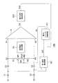
図1に示すように、入力回路100は、第1の入力端子T1と、第2の入力端子T2と、第1の容量C1と、第2の容量C2と、基準電圧発生回路VGと、第1の抵抗R1と、第2の抵抗R2と、第1のスイッチSW1と、第2のスイッチSW2と、差動受信回路Aと、第1のスイッチ制御回路SC1と、第1の信号検出回路DC1と、第2の信号検出回路DC2と、を備える。
図2は、図1に示す入力回路100に入力される信号波形と各ノードの信号波形を示す図である。また、図3は、図1に示す入力回路100の第1、第2のノードN1、N2の信号波形(EYE波形)の一例を示す図である。
図4は、第2の実施形態に係る入力回路200の構成の一例を示す回路図である。なお、この図4において、図1の符号と同じ符号は、第1の実施形態と同様の構成を示す。
第2のスイッチ制御回路SC2は、第1の検出信号Sd1に応じて、第3のスイッチSW3および第4のスイッチSW4をオンし、且つ、第5のスイッチSW5および第6のスイッチSW6をオフする。
T1 第1の入力端子
T2 第2の入力端子
C1 第1の容量
C2 第2の容量
VG 基準電圧発生回路
R1 第1の抵抗
R2 第2の抵抗
SW1 第1のスイッチ
SW2 第2のスイッチ
A 差動受信回路
SC1 第1のスイッチ制御回路
SC2 第2のスイッチ制御回路
DC1 第1の信号検出回路
DC2 第2の信号検出回路
Claims (8)
- 第1の入力信号が入力される第1の入力端子と、
前記第1の入力信号の位相を反転した第2の入力信号が入力される第2の入力端子と、 一端が前記第1の入力端子に接続され、他端が第1のノードに接続された第1の容量と、
一端が前記第2の入力端子に接続され、他端が第2のノードに接続された第2の容量と、
基準電圧を発生して基準ノードに供給する基準電圧発生回路と、
前記第1のノードと前記基準ノードとの間に接続された第1の抵抗と、
前記第2のノードと前記基準ノードとの間に接続された第2の抵抗と、
前記第1のノードと前記基準ノードとの間で、前記第1の抵抗と直列に接続された第1のスイッチと、
前記第2のノードと前記基準ノードとの間で、前記第2の抵抗と直列に接続された第2のスイッチと、
第1の入力部が前記第1のノードに接続され、第2の入力部が前記第2のノードに接続され、前記第1の入力部および前記第2の入力部に入力される差動信号を受信し、単相の出力信号を出力する差動受信回路と、
前記第1のスイッチおよび前記第2のスイッチを制御する第1のスイッチ制御回路と、を備え、
前記第1のスイッチ制御回路は、
前記第1の入力信号および前記第2の入力信号がDC信号である第1の期間において、前記第1のスイッチおよび前記第2のスイッチをオフして、前記第1のノードと前記基準ノードとの間を電気的に遮断するとともに、前記第2のノードと前記基準ノードとの間を電気的に遮断し、
前記第1の入力信号および前記第2の入力信号がAC信号である第2の期間において、前記第1のスイッチおよび前記第2のスイッチをオンして、前記第1のノードと前記基準ノードとの間を電気的に導通するとともに、前記第2のノードと前記基準ノードとの間を電気的に導通する
入力回路。 - 前記DC信号は、予め設定された規定期間において、同じビットが連続する数が予め規定された規定数以上の信号であり、
前記AC信号は、前記規定期間において、同じビットが連続する数が前記規定数未満である信号である
請求項1に記載の入力回路。 - 前記AC信号は、前記規定期間において、“1”と“0”の割合が1:1である請求項2に記載の入力回路。
- 前記第1の入力端子を介して前記第1の入力信号が入力され且つ前記第2の入力端子を介して前記第2の入力信号が入力され、前記第1の入力信号および前記第2の入力信号に基づいて検出信号を出力する第1の信号検出回路をさらに備え、
前記第1の信号検出回路は、前記第1の入力信号および前記第2の入力信号が前記DC信号であることを検出した場合には、第1の検出信号を出力し、
前記第1のスイッチ制御回路は、前記第1の検出信号に応じて、前記第1のスイッチおよび前記第2のスイッチをオフする、
請求項1から3のいずれか一項に記載の入力回路。 - 前記差動受信回路の前記出力信号が入力され、前記出力信号に基づいて検出信号を出力する第2の信号検出回路をさらに備え、
前記第2の信号検出回路は、前記出力信号が前記AC信号になったことを検出した場合には、第2の検出信号を出力し、
前記第1のスイッチ制御回路は、前記第2の検出信号に応じて、前記第1のスイッチおよび前記第2のスイッチをオンする
請求項4に記載の入力回路。 - 前記第1の入力端子と前記第1の容量の一端との間に接続された第3のスイッチと、
前記第2の入力端子と前記第2の容量の一端との間に接続された第4のスイッチと、
一端が前記第1の入力端子に接続された第3の抵抗と、
一端が前記第2の入力端子に接続され、他端が前記第3の抵抗の他端に接続された第4の抵抗と、
一端が前記第3の抵抗の他端に接続された第5の抵抗と、
一端が前記第5の抵抗の他端に接続され、他端が前記第1の容量の一端に接続された第5のスイッチと、
一端が前記第5の抵抗の他端に接続され、他端が前記第2の容量の一端に接続された第6のスイッチと、
前記第3のスイッチ、前記第4のスイッチ、前記第5のスイッチ、および、前記第6のスイッチを制御する第2のスイッチ制御回路と、を備え、
前記第2のスイッチ制御回路は、
前記第1の期間のうち、前記第2の期間の直前の前記第1の入力信号および前記第2の入力信号が前記DC信号を構成する固定信号である期間、および、前記第2の期間において、前記第3のスイッチおよび前記第4のスイッチをオンし、且つ、前記第5のスイッチおよび前記第6のスイッチをオフし、
前記第1の期間のうち、前記第1の入力信号および前記第2の入力信号が前記DC信号を構成する反転信号である期間は、前記第3のスイッチおよび前記第4のスイッチをオフし、且つ、前記第5のスイッチおよび前記第6のスイッチをオンする
請求項1に記載の入力回路。 - 前記第1の入力端子を介して前記第1の入力信号が入力され且つ前記第2の入力端子を介して前記第2の入力信号が入力され、前記第1の入力信号および前記第2の入力信号に基づいて検出信号を出力する第1の信号検出回路をさらに備え、
前記第1の信号検出回路は、前記第1の期間の直前の前記第1の入力信号および前記第2の入力信号が固定信号になったことを検出した場合には、第1の検出信号を出力し、
前記第1のスイッチ制御回路は、前記第1の検出信号に応じて、前記第1のスイッチおよび前記第2のスイッチをオフする
請求項6に記載の入力回路。 - 前記第2のスイッチ制御回路は、
前記第1の信号検出回路から前記第1の検出信号が出力される前において、前記第3のスイッチおよび前記第4のスイッチをオフし、且つ、前記第5のスイッチおよび前記第6のスイッチをオンし、
前記第1の検出信号に応じて、前記第3のスイッチおよび前記第4のスイッチをオンし、且つ、前記第5のスイッチおよび前記第6のスイッチをオフする
請求項7に記載の入力回路。
Priority Applications (2)
| Application Number | Priority Date | Filing Date | Title |
|---|---|---|---|
| JP2014012689A JP6110799B2 (ja) | 2014-01-27 | 2014-01-27 | 入力回路 |
| US14/476,217 US9525404B2 (en) | 2014-01-27 | 2014-09-03 | Input circuit |
Applications Claiming Priority (1)
| Application Number | Priority Date | Filing Date | Title |
|---|---|---|---|
| JP2014012689A JP6110799B2 (ja) | 2014-01-27 | 2014-01-27 | 入力回路 |
Publications (2)
| Publication Number | Publication Date |
|---|---|
| JP2015142174A JP2015142174A (ja) | 2015-08-03 |
| JP6110799B2 true JP6110799B2 (ja) | 2017-04-05 |
Family
ID=53680051
Family Applications (1)
| Application Number | Title | Priority Date | Filing Date |
|---|---|---|---|
| JP2014012689A Expired - Fee Related JP6110799B2 (ja) | 2014-01-27 | 2014-01-27 | 入力回路 |
Country Status (2)
| Country | Link |
|---|---|
| US (1) | US9525404B2 (ja) |
| JP (1) | JP6110799B2 (ja) |
Families Citing this family (1)
| Publication number | Priority date | Publication date | Assignee | Title |
|---|---|---|---|---|
| US10198682B2 (en) | 2016-09-13 | 2019-02-05 | Toshiba Memory Corporation | Receiving system and memory card |
Family Cites Families (17)
| Publication number | Priority date | Publication date | Assignee | Title |
|---|---|---|---|---|
| DE69227027T2 (de) * | 1991-03-29 | 1999-04-15 | Ericsson Raynet | Empfänger mit klemmschaltung und entsprechendes optisches kommunikationsnetz |
| US5844431A (en) * | 1996-09-18 | 1998-12-01 | Exar Corporation | Low noise low power CMOS correlated double sampler |
| JPH1188364A (ja) | 1997-09-16 | 1999-03-30 | Matsushita Electric Ind Co Ltd | 通信装置 |
| US6078613A (en) * | 1997-12-23 | 2000-06-20 | Paradyne Corporation | System and method for bridging multiple communication devices to a single communication connection |
| JP2003179639A (ja) | 2002-11-11 | 2003-06-27 | Matsushita Electric Ind Co Ltd | 通信装置 |
| US7084700B2 (en) * | 2003-04-17 | 2006-08-01 | Fujitsu Limited | Differential voltage amplifier circuit |
| US8346198B2 (en) * | 2005-06-30 | 2013-01-01 | Silicon Laboratories Inc. | Low noise amplifier for a radio receiver |
| US7417462B1 (en) * | 2007-03-20 | 2008-08-26 | Altera Corporation | Variable external interface circuitry on programmable logic device integrated circuits |
| JP2009038546A (ja) | 2007-08-01 | 2009-02-19 | Panasonic Corp | 電流ドライバ |
| US7649409B1 (en) * | 2007-10-23 | 2010-01-19 | National Semiconductor Corporation | All-pass termination network with equalization and wide common-mode range |
| US20100278226A1 (en) * | 2009-05-04 | 2010-11-04 | Advantest Corporation | Transmission circuit, differential signal transmission circuit, and test apparatus |
| JP2011010244A (ja) * | 2009-06-29 | 2011-01-13 | Hitachi-Lg Data Storage Inc | 情報検出装置及び方法 |
| JP2011130281A (ja) | 2009-12-18 | 2011-06-30 | Thine Electronics Inc | 受信装置および送受信システム |
| JP2012100017A (ja) | 2010-11-01 | 2012-05-24 | Renesas Electronics Corp | 半導体集積回路およびその動作方法 |
| US8319579B2 (en) * | 2010-11-29 | 2012-11-27 | Advanced Micro Devices, Inc. | Passive filter and AC coupler receiver interface |
| TWI469510B (zh) * | 2012-10-09 | 2015-01-11 | Novatek Microelectronics Corp | 介面電路 |
| US9584184B2 (en) * | 2013-03-05 | 2017-02-28 | Qualcomm Incorporated | Unified front-end receiver interface for accommodating incoming signals via AC-coupling or DC-coupling |
-
2014
- 2014-01-27 JP JP2014012689A patent/JP6110799B2/ja not_active Expired - Fee Related
- 2014-09-03 US US14/476,217 patent/US9525404B2/en active Active
Also Published As
| Publication number | Publication date |
|---|---|
| US20150214935A1 (en) | 2015-07-30 |
| US9525404B2 (en) | 2016-12-20 |
| JP2015142174A (ja) | 2015-08-03 |
Similar Documents
| Publication | Publication Date | Title |
|---|---|---|
| US11368332B2 (en) | Circuit device, electronic device, and cable harness | |
| KR102071573B1 (ko) | 외부 클락 신호를 이용하여 오실레이터의 주파수를 조절할 수 있는 디스플레이 드라이버 ic, 이를 포함하는 장치, 및 이들의 동작 방법 | |
| JP2015228554A5 (ja) | ||
| US10523259B2 (en) | Transmitter and communication system | |
| US20120280721A1 (en) | Squelch detection circuit | |
| TW201630387A (zh) | 用於數位地取消串擾之裝置及方法 | |
| JP2015219692A (ja) | スレーブ通信装置及びバス通信システム | |
| US7292073B2 (en) | Transmission line driver circuit | |
| JP6110799B2 (ja) | 入力回路 | |
| JP2013225281A (ja) | 処理装置及び処理システム | |
| JP2020522909A (ja) | 電流検出器及び制御論理回路を用いるオープンドレイン通信システムのための中継器 | |
| KR20190033195A (ko) | 터미네이션 회로 및 인터페이스 장치 | |
| JP5876799B2 (ja) | 半導体装置 | |
| JP5444911B2 (ja) | 送受信制御装置、電子機器、データ送信方法及び制御プログラム | |
| US10644695B1 (en) | Source driver | |
| JP6900780B2 (ja) | 回路装置、電子機器及びケーブルハーネス | |
| JP6904210B2 (ja) | 回路装置、電子機器及びケーブルハーネス | |
| JP3726911B2 (ja) | 送信回路、データ転送制御装置及び電子機器 | |
| US11489524B2 (en) | Semiconductor device | |
| US7760211B2 (en) | System and method for light control | |
| JP2014116925A (ja) | パワーオンリセット回路 | |
| KR20190018365A (ko) | 2선 무극선 통신시스템 | |
| TWI683199B (zh) | 適應性放電電路以及電源供應器 | |
| US10015026B2 (en) | Transmitter and communication system | |
| JP2006042218A (ja) | 半導体集積回路 |
Legal Events
| Date | Code | Title | Description |
|---|---|---|---|
| A621 | Written request for application examination |
Free format text: JAPANESE INTERMEDIATE CODE: A621 Effective date: 20160219 |
|
| A977 | Report on retrieval |
Free format text: JAPANESE INTERMEDIATE CODE: A971007 Effective date: 20161124 |
|
| A131 | Notification of reasons for refusal |
Free format text: JAPANESE INTERMEDIATE CODE: A131 Effective date: 20161202 |
|
| A521 | Written amendment |
Free format text: JAPANESE INTERMEDIATE CODE: A523 Effective date: 20170130 |
|
| TRDD | Decision of grant or rejection written | ||
| A01 | Written decision to grant a patent or to grant a registration (utility model) |
Free format text: JAPANESE INTERMEDIATE CODE: A01 Effective date: 20170210 |
|
| A61 | First payment of annual fees (during grant procedure) |
Free format text: JAPANESE INTERMEDIATE CODE: A61 Effective date: 20170310 |
|
| R151 | Written notification of patent or utility model registration |
Ref document number: 6110799 Country of ref document: JP Free format text: JAPANESE INTERMEDIATE CODE: R151 |
|
| LAPS | Cancellation because of no payment of annual fees |