JP6087058B2 - 半導体装置 - Google Patents
半導体装置 Download PDFInfo
- Publication number
- JP6087058B2 JP6087058B2 JP2012007604A JP2012007604A JP6087058B2 JP 6087058 B2 JP6087058 B2 JP 6087058B2 JP 2012007604 A JP2012007604 A JP 2012007604A JP 2012007604 A JP2012007604 A JP 2012007604A JP 6087058 B2 JP6087058 B2 JP 6087058B2
- Authority
- JP
- Japan
- Prior art keywords
- floating gate
- insulating film
- control gate
- work function
- gate insulating
- Prior art date
- Legal status (The legal status is an assumption and is not a legal conclusion. Google has not performed a legal analysis and makes no representation as to the accuracy of the status listed.)
- Expired - Fee Related
Links
- 239000004065 semiconductor Substances 0.000 title claims description 71
- IJGRMHOSHXDMSA-UHFFFAOYSA-N Atomic nitrogen Chemical compound N#N IJGRMHOSHXDMSA-UHFFFAOYSA-N 0.000 claims description 30
- 229910052757 nitrogen Inorganic materials 0.000 claims description 15
- QVGXLLKOCUKJST-UHFFFAOYSA-N atomic oxygen Chemical compound [O] QVGXLLKOCUKJST-UHFFFAOYSA-N 0.000 claims description 14
- 229910052760 oxygen Inorganic materials 0.000 claims description 14
- 239000001301 oxygen Substances 0.000 claims description 14
- APFVFJFRJDLVQX-UHFFFAOYSA-N indium atom Chemical compound [In] APFVFJFRJDLVQX-UHFFFAOYSA-N 0.000 claims description 12
- 239000011701 zinc Substances 0.000 claims description 12
- 229910052738 indium Inorganic materials 0.000 claims description 11
- HCHKCACWOHOZIP-UHFFFAOYSA-N Zinc Chemical compound [Zn] HCHKCACWOHOZIP-UHFFFAOYSA-N 0.000 claims description 10
- 229910052725 zinc Inorganic materials 0.000 claims description 10
- 239000010408 film Substances 0.000 description 116
- 230000006870 function Effects 0.000 description 66
- 150000001875 compounds Chemical class 0.000 description 43
- 239000000758 substrate Substances 0.000 description 43
- 239000000463 material Substances 0.000 description 31
- 239000012535 impurity Substances 0.000 description 28
- 238000000034 method Methods 0.000 description 23
- 230000004888 barrier function Effects 0.000 description 22
- 230000000694 effects Effects 0.000 description 20
- 210000004027 cell Anatomy 0.000 description 13
- GYHNNYVSQQEPJS-UHFFFAOYSA-N Gallium Chemical compound [Ga] GYHNNYVSQQEPJS-UHFFFAOYSA-N 0.000 description 12
- 229910052733 gallium Inorganic materials 0.000 description 12
- 229910000449 hafnium oxide Inorganic materials 0.000 description 12
- WIHZLLGSGQNAGK-UHFFFAOYSA-N hafnium(4+);oxygen(2-) Chemical compound [O-2].[O-2].[Hf+4] WIHZLLGSGQNAGK-UHFFFAOYSA-N 0.000 description 12
- VYPSYNLAJGMNEJ-UHFFFAOYSA-N Silicium dioxide Chemical compound O=[Si]=O VYPSYNLAJGMNEJ-UHFFFAOYSA-N 0.000 description 10
- XUIMIQQOPSSXEZ-UHFFFAOYSA-N Silicon Chemical compound [Si] XUIMIQQOPSSXEZ-UHFFFAOYSA-N 0.000 description 10
- 229910007541 Zn O Inorganic materials 0.000 description 10
- 230000005684 electric field Effects 0.000 description 10
- 125000005843 halogen group Chemical group 0.000 description 10
- 229910052710 silicon Inorganic materials 0.000 description 10
- 239000010703 silicon Substances 0.000 description 10
- 229910052814 silicon oxide Inorganic materials 0.000 description 10
- 229910052751 metal Inorganic materials 0.000 description 9
- NWAIGJYBQQYSPW-UHFFFAOYSA-N azanylidyneindigane Chemical group [In]#N NWAIGJYBQQYSPW-UHFFFAOYSA-N 0.000 description 8
- MRELNEQAGSRDBK-UHFFFAOYSA-N lanthanum(3+);oxygen(2-) Chemical compound [O-2].[O-2].[O-2].[La+3].[La+3] MRELNEQAGSRDBK-UHFFFAOYSA-N 0.000 description 8
- 238000004519 manufacturing process Methods 0.000 description 8
- PMHQVHHXPFUNSP-UHFFFAOYSA-M copper(1+);methylsulfanylmethane;bromide Chemical compound Br[Cu].CSC PMHQVHHXPFUNSP-UHFFFAOYSA-M 0.000 description 7
- AJNVQOSZGJRYEI-UHFFFAOYSA-N digallium;oxygen(2-) Chemical compound [O-2].[O-2].[O-2].[Ga+3].[Ga+3] AJNVQOSZGJRYEI-UHFFFAOYSA-N 0.000 description 7
- 229910001195 gallium oxide Inorganic materials 0.000 description 7
- NJWNEWQMQCGRDO-UHFFFAOYSA-N indium zinc Chemical compound [Zn].[In] NJWNEWQMQCGRDO-UHFFFAOYSA-N 0.000 description 7
- 239000002184 metal Substances 0.000 description 7
- 239000003990 capacitor Substances 0.000 description 6
- 239000012212 insulator Substances 0.000 description 6
- 238000002955 isolation Methods 0.000 description 6
- 229910021421 monocrystalline silicon Inorganic materials 0.000 description 6
- XLOMVQKBTHCTTD-UHFFFAOYSA-N zinc oxide Inorganic materials [Zn]=O XLOMVQKBTHCTTD-UHFFFAOYSA-N 0.000 description 6
- 229910052984 zinc sulfide Inorganic materials 0.000 description 6
- 239000000969 carrier Substances 0.000 description 5
- 239000013078 crystal Substances 0.000 description 5
- 229910052735 hafnium Inorganic materials 0.000 description 5
- VBJZVLUMGGDVMO-UHFFFAOYSA-N hafnium atom Chemical compound [Hf] VBJZVLUMGGDVMO-UHFFFAOYSA-N 0.000 description 5
- UFHFLCQGNIYNRP-UHFFFAOYSA-N Hydrogen Chemical compound [H][H] UFHFLCQGNIYNRP-UHFFFAOYSA-N 0.000 description 4
- BPQQTUXANYXVAA-UHFFFAOYSA-N Orthosilicate Chemical compound [O-][Si]([O-])([O-])[O-] BPQQTUXANYXVAA-UHFFFAOYSA-N 0.000 description 4
- 229910052782 aluminium Inorganic materials 0.000 description 4
- XAGFODPZIPBFFR-UHFFFAOYSA-N aluminium Chemical compound [Al] XAGFODPZIPBFFR-UHFFFAOYSA-N 0.000 description 4
- 230000015572 biosynthetic process Effects 0.000 description 4
- 238000005229 chemical vapour deposition Methods 0.000 description 4
- 239000001257 hydrogen Substances 0.000 description 4
- 229910052739 hydrogen Inorganic materials 0.000 description 4
- TWNQGVIAIRXVLR-UHFFFAOYSA-N oxo(oxoalumanyloxy)alumane Chemical compound O=[Al]O[Al]=O TWNQGVIAIRXVLR-UHFFFAOYSA-N 0.000 description 4
- SIWVEOZUMHYXCS-UHFFFAOYSA-N oxo(oxoyttriooxy)yttrium Chemical compound O=[Y]O[Y]=O SIWVEOZUMHYXCS-UHFFFAOYSA-N 0.000 description 4
- BPUBBGLMJRNUCC-UHFFFAOYSA-N oxygen(2-);tantalum(5+) Chemical compound [O-2].[O-2].[O-2].[O-2].[O-2].[Ta+5].[Ta+5] BPUBBGLMJRNUCC-UHFFFAOYSA-N 0.000 description 4
- RVTZCBVAJQQJTK-UHFFFAOYSA-N oxygen(2-);zirconium(4+) Chemical compound [O-2].[O-2].[Zr+4] RVTZCBVAJQQJTK-UHFFFAOYSA-N 0.000 description 4
- 229910001936 tantalum oxide Inorganic materials 0.000 description 4
- 239000011787 zinc oxide Substances 0.000 description 4
- 229910001928 zirconium oxide Inorganic materials 0.000 description 4
- GFQYVLUOOAAOGM-UHFFFAOYSA-N zirconium(iv) silicate Chemical compound [Zr+4].[O-][Si]([O-])([O-])[O-] GFQYVLUOOAAOGM-UHFFFAOYSA-N 0.000 description 4
- RTAQQCXQSZGOHL-UHFFFAOYSA-N Titanium Chemical compound [Ti] RTAQQCXQSZGOHL-UHFFFAOYSA-N 0.000 description 3
- 230000007547 defect Effects 0.000 description 3
- 238000005468 ion implantation Methods 0.000 description 3
- 150000002736 metal compounds Chemical class 0.000 description 3
- 229910044991 metal oxide Inorganic materials 0.000 description 3
- 150000004706 metal oxides Chemical class 0.000 description 3
- 230000000717 retained effect Effects 0.000 description 3
- 229910052715 tantalum Inorganic materials 0.000 description 3
- GUVRBAGPIYLISA-UHFFFAOYSA-N tantalum atom Chemical compound [Ta] GUVRBAGPIYLISA-UHFFFAOYSA-N 0.000 description 3
- 229910052719 titanium Inorganic materials 0.000 description 3
- 239000010936 titanium Substances 0.000 description 3
- AKJVMGQSGCSQBU-UHFFFAOYSA-N zinc azanidylidenezinc Chemical group [Zn++].[N-]=[Zn].[N-]=[Zn] AKJVMGQSGCSQBU-UHFFFAOYSA-N 0.000 description 3
- QGZKDVFQNNGYKY-UHFFFAOYSA-N Ammonia Chemical compound N QGZKDVFQNNGYKY-UHFFFAOYSA-N 0.000 description 2
- -1 In—Sn—O Chemical class 0.000 description 2
- UORVGPXVDQYIDP-UHFFFAOYSA-N borane Chemical compound B UORVGPXVDQYIDP-UHFFFAOYSA-N 0.000 description 2
- 229910052796 boron Inorganic materials 0.000 description 2
- 238000005516 engineering process Methods 0.000 description 2
- 239000007789 gas Substances 0.000 description 2
- 238000005984 hydrogenation reaction Methods 0.000 description 2
- 230000007246 mechanism Effects 0.000 description 2
- 239000000203 mixture Substances 0.000 description 2
- 238000001451 molecular beam epitaxy Methods 0.000 description 2
- 230000008569 process Effects 0.000 description 2
- 238000004544 sputter deposition Methods 0.000 description 2
- 239000000126 substance Substances 0.000 description 2
- 229960001296 zinc oxide Drugs 0.000 description 2
- JBRZTFJDHDCESZ-UHFFFAOYSA-N AsGa Chemical compound [As]#[Ga] JBRZTFJDHDCESZ-UHFFFAOYSA-N 0.000 description 1
- ZOXJGFHDIHLPTG-UHFFFAOYSA-N Boron Chemical compound [B] ZOXJGFHDIHLPTG-UHFFFAOYSA-N 0.000 description 1
- 229910001218 Gallium arsenide Inorganic materials 0.000 description 1
- 229910020923 Sn-O Inorganic materials 0.000 description 1
- NRTOMJZYCJJWKI-UHFFFAOYSA-N Titanium nitride Chemical compound [Ti]#N NRTOMJZYCJJWKI-UHFFFAOYSA-N 0.000 description 1
- QCWXUUIWCKQGHC-UHFFFAOYSA-N Zirconium Chemical compound [Zr] QCWXUUIWCKQGHC-UHFFFAOYSA-N 0.000 description 1
- 229910045601 alloy Inorganic materials 0.000 description 1
- 239000000956 alloy Substances 0.000 description 1
- 229910021529 ammonia Inorganic materials 0.000 description 1
- 229910052785 arsenic Inorganic materials 0.000 description 1
- RQNWIZPPADIBDY-UHFFFAOYSA-N arsenic atom Chemical compound [As] RQNWIZPPADIBDY-UHFFFAOYSA-N 0.000 description 1
- 125000004429 atom Chemical group 0.000 description 1
- 229910052788 barium Inorganic materials 0.000 description 1
- DSAJWYNOEDNPEQ-UHFFFAOYSA-N barium atom Chemical compound [Ba] DSAJWYNOEDNPEQ-UHFFFAOYSA-N 0.000 description 1
- 230000008901 benefit Effects 0.000 description 1
- 229910052797 bismuth Inorganic materials 0.000 description 1
- JCXGWMGPZLAOME-UHFFFAOYSA-N bismuth atom Chemical compound [Bi] JCXGWMGPZLAOME-UHFFFAOYSA-N 0.000 description 1
- 229910000085 borane Inorganic materials 0.000 description 1
- 230000015556 catabolic process Effects 0.000 description 1
- 239000004020 conductor Substances 0.000 description 1
- 230000007423 decrease Effects 0.000 description 1
- 230000003247 decreasing effect Effects 0.000 description 1
- 238000000151 deposition Methods 0.000 description 1
- 230000008021 deposition Effects 0.000 description 1
- 238000005530 etching Methods 0.000 description 1
- 239000010419 fine particle Substances 0.000 description 1
- VTGARNNDLOTBET-UHFFFAOYSA-N gallium antimonide Chemical compound [Sb]#[Ga] VTGARNNDLOTBET-UHFFFAOYSA-N 0.000 description 1
- 229910052732 germanium Inorganic materials 0.000 description 1
- GNPVGFCGXDBREM-UHFFFAOYSA-N germanium atom Chemical compound [Ge] GNPVGFCGXDBREM-UHFFFAOYSA-N 0.000 description 1
- 238000010438 heat treatment Methods 0.000 description 1
- 125000004435 hydrogen atom Chemical group [H]* 0.000 description 1
- 229910003437 indium oxide Inorganic materials 0.000 description 1
- PJXISJQVUVHSOJ-UHFFFAOYSA-N indium(iii) oxide Chemical compound [O-2].[O-2].[O-2].[In+3].[In+3] PJXISJQVUVHSOJ-UHFFFAOYSA-N 0.000 description 1
- 230000001939 inductive effect Effects 0.000 description 1
- 230000010354 integration Effects 0.000 description 1
- 238000007733 ion plating Methods 0.000 description 1
- 150000002500 ions Chemical class 0.000 description 1
- 229910052746 lanthanum Inorganic materials 0.000 description 1
- FZLIPJUXYLNCLC-UHFFFAOYSA-N lanthanum atom Chemical compound [La] FZLIPJUXYLNCLC-UHFFFAOYSA-N 0.000 description 1
- 230000014759 maintenance of location Effects 0.000 description 1
- 150000002739 metals Chemical class 0.000 description 1
- 239000002070 nanowire Substances 0.000 description 1
- 150000004767 nitrides Chemical class 0.000 description 1
- 230000003647 oxidation Effects 0.000 description 1
- 238000007254 oxidation reaction Methods 0.000 description 1
- 230000001590 oxidative effect Effects 0.000 description 1
- 230000000704 physical effect Effects 0.000 description 1
- 229910021420 polycrystalline silicon Inorganic materials 0.000 description 1
- 238000005546 reactive sputtering Methods 0.000 description 1
- 238000006479 redox reaction Methods 0.000 description 1
- 230000009467 reduction Effects 0.000 description 1
- 238000006722 reduction reaction Methods 0.000 description 1
- 239000007787 solid Substances 0.000 description 1
- 230000000087 stabilizing effect Effects 0.000 description 1
- 210000000352 storage cell Anatomy 0.000 description 1
- 229910052712 strontium Inorganic materials 0.000 description 1
- CIOAGBVUUVVLOB-UHFFFAOYSA-N strontium atom Chemical compound [Sr] CIOAGBVUUVVLOB-UHFFFAOYSA-N 0.000 description 1
- MZLGASXMSKOWSE-UHFFFAOYSA-N tantalum nitride Chemical compound [Ta]#N MZLGASXMSKOWSE-UHFFFAOYSA-N 0.000 description 1
- JBQYATWDVHIOAR-UHFFFAOYSA-N tellanylidenegermanium Chemical compound [Te]=[Ge] JBQYATWDVHIOAR-UHFFFAOYSA-N 0.000 description 1
- 239000010409 thin film Substances 0.000 description 1
- XCZXGTMEAKBVPV-UHFFFAOYSA-N trimethylgallium Chemical compound C[Ga](C)C XCZXGTMEAKBVPV-UHFFFAOYSA-N 0.000 description 1
- IBEFSUTVZWZJEL-UHFFFAOYSA-N trimethylindium Chemical compound C[In](C)C IBEFSUTVZWZJEL-UHFFFAOYSA-N 0.000 description 1
- WFKWXMTUELFFGS-UHFFFAOYSA-N tungsten Chemical compound [W] WFKWXMTUELFFGS-UHFFFAOYSA-N 0.000 description 1
- 229910052721 tungsten Inorganic materials 0.000 description 1
- 239000010937 tungsten Substances 0.000 description 1
- 238000001771 vacuum deposition Methods 0.000 description 1
- 229910052727 yttrium Inorganic materials 0.000 description 1
- VWQVUPCCIRVNHF-UHFFFAOYSA-N yttrium atom Chemical compound [Y] VWQVUPCCIRVNHF-UHFFFAOYSA-N 0.000 description 1
- YVTHLONGBIQYBO-UHFFFAOYSA-N zinc indium(3+) oxygen(2-) Chemical compound [O--].[Zn++].[In+3] YVTHLONGBIQYBO-UHFFFAOYSA-N 0.000 description 1
- 229910052726 zirconium Inorganic materials 0.000 description 1
Images


Landscapes
- Semiconductor Memories (AREA)
- Non-Volatile Memory (AREA)
Description
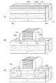
図2(A)に、本実施の形態のFGメモリ装置の例を図示する。ここでは、トランジスタのチャネル方向の断面模式図を示す。トランジスタはp型の単結晶珪素の基板100上にフローティングゲート103と基板100との間に適切な厚さのフローティングゲート絶縁膜105を有する。
図3(A)に、本実施の形態のFGメモリ装置の例を図示する。なお、一部の記載については実施の形態1を参酌できる。ここでは、トランジスタのチャネル方向の断面模式図を示す。トランジスタはn型の単結晶珪素の基板200上にフローティングゲート203と、基板200との間に適切な厚さのフローティングゲート絶縁膜205を有する。
図3(B)と図3(C)の特徴を併せ持つFGメモリ装置の作製方法の例について図4を用いて簡単に説明する。なお、多くの工程は公知の半導体技術を用いればよいので詳細はそれらを参照できる。
101 素子分離絶縁物
102 不純物領域
102a ソース
102b ドレイン
103 フローティングゲート
103a フローティングゲートの第1導電層
103b フローティングゲートの第2導電層
104 コントロールゲート
104a コントロールゲートの第1導電層
104b コントロールゲートの第2導電層
105 フローティングゲート絶縁膜
106 コントロールゲート絶縁膜
107 n型領域
108a ハロー領域
108b ハロー領域
200 基板
201 素子分離絶縁物
202a ソース
202b ドレイン
203 フローティングゲート
203a フローティングゲートの第1導電層
203b フローティングゲートの第2導電層
203c 高仕事関数酸窒化物層
204 コントロールゲート
204a コントロールゲートの第1導電層
204b コントロールゲートの第2導電層
205a 絶縁膜
205 フローティングゲート絶縁膜
206 コントロールゲート絶縁膜
207 弱いn型領域
208 n型領域
209a 側壁
209b 側壁
Claims (3)
- 半導体領域と、
前記半導体領域上の、第1の絶縁膜と、
前記第1の絶縁膜上の、フローティングゲートと、
前記フローティングゲート上の、第2の絶縁膜と、
前記第2の絶縁膜上の、コントロールゲートと、を有し、
前記フローティングゲートは、インジウム又は亜鉛の少なくとも一と、酸素と、窒素とを有し、
前記酸素は、前記窒素の2倍乃至5倍で含有され、
前記第2の絶縁膜の比誘電率は10以上であることを特徴とする半導体装置。 - 半導体領域と、
前記半導体領域上の、第1の絶縁膜と、
前記第1の絶縁膜上の、フローティングゲートと、
前記フローティングゲート上の、第2の絶縁膜と、
前記第2の絶縁膜上の、コントロールゲートと、を有し、
前記フローティングゲートは、第1の導電層と、前記第1の導電層上の第2の導電層とを有し、
前記第2の導電層は、インジウム又は亜鉛の少なくとも一と、酸素と、窒素とを有し、
前記酸素は、前記窒素の2倍乃至5倍で含有され、
前記第2の絶縁膜の比誘電率は10以上であることを特徴とする半導体装置。 - 半導体領域と、
前記半導体領域上の、第1の絶縁膜と、
前記第1の絶縁膜上の、フローティングゲートと、
前記フローティングゲート上の、第2の絶縁膜と、
前記第2の絶縁膜上の、コントロールゲートと、を有し、
前記フローティングゲートは、インジウム又は亜鉛の少なくとも一と、酸素と、窒素とを有し、
前記コントロールゲートは、インジウム又は亜鉛の少なくとも一と、窒素とを有し、
前記フローティングゲートにおいて、前記酸素は、前記窒素の2倍乃至5倍で含有され、
前記第2の絶縁膜の比誘電率は10以上であることを特徴とする半導体装置。
Priority Applications (1)
| Application Number | Priority Date | Filing Date | Title |
|---|---|---|---|
| JP2012007604A JP6087058B2 (ja) | 2012-01-18 | 2012-01-18 | 半導体装置 |
Applications Claiming Priority (1)
| Application Number | Priority Date | Filing Date | Title |
|---|---|---|---|
| JP2012007604A JP6087058B2 (ja) | 2012-01-18 | 2012-01-18 | 半導体装置 |
Publications (3)
| Publication Number | Publication Date |
|---|---|
| JP2013149693A JP2013149693A (ja) | 2013-08-01 |
| JP2013149693A5 JP2013149693A5 (ja) | 2015-02-26 |
| JP6087058B2 true JP6087058B2 (ja) | 2017-03-01 |
Family
ID=49046939
Family Applications (1)
| Application Number | Title | Priority Date | Filing Date |
|---|---|---|---|
| JP2012007604A Expired - Fee Related JP6087058B2 (ja) | 2012-01-18 | 2012-01-18 | 半導体装置 |
Country Status (1)
| Country | Link |
|---|---|
| JP (1) | JP6087058B2 (ja) |
Family Cites Families (2)
| Publication number | Priority date | Publication date | Assignee | Title |
|---|---|---|---|---|
| JP3142823U (ja) * | 2008-04-17 | 2008-06-26 | 有限会社ウェルシー | 枕 |
| JP3154563U (ja) * | 2009-07-31 | 2009-10-22 | 株式会社タナカふとんサービス | 寝具用枕 |
-
2012
- 2012-01-18 JP JP2012007604A patent/JP6087058B2/ja not_active Expired - Fee Related
Also Published As
| Publication number | Publication date |
|---|---|
| JP2013149693A (ja) | 2013-08-01 |
Similar Documents
| Publication | Publication Date | Title |
|---|---|---|
| US7978504B2 (en) | Floating gate device with graphite floating gate | |
| US7928502B2 (en) | Transistor devices with nano-crystal gate structures | |
| JP6087057B2 (ja) | 半導体メモリ装置 | |
| US11824118B2 (en) | Electronic device and method of manufacturing the same | |
| US9305650B2 (en) | Junction field-effect floating gate memory switch with thin tunnel insulator | |
| JP2009135494A (ja) | 消去飽和について改善したイミュニティを備えた不揮発性メモリデバイスおよびその製造方法 | |
| KR100761180B1 (ko) | 불휘발성 반도체 기억 장치 및 그 제조 방법 | |
| US20230122250A1 (en) | Field effect transistor with multiple hybrid fin structure and method | |
| JP6088142B2 (ja) | 半導体装置 | |
| JP6087058B2 (ja) | 半導体装置 | |
| JP2025521671A (ja) | 薄膜トランジスタ及び薄膜トランジスタの製造方法 | |
| JP6411556B2 (ja) | 半導体メモリ装置 | |
| KR101060617B1 (ko) | 비휘발성 메모리 소자 및 그 제조 방법 | |
| US10910476B2 (en) | Integrated structures having gallium-containing regions | |
| US20250048683A1 (en) | Methods of forming electronic devices having a strained transistor channel | |
| JP5189309B2 (ja) | 絶縁ゲート型半導体装置及びその製造方法 |
Legal Events
| Date | Code | Title | Description |
|---|---|---|---|
| A521 | Request for written amendment filed |
Free format text: JAPANESE INTERMEDIATE CODE: A523 Effective date: 20150108 |
|
| A621 | Written request for application examination |
Free format text: JAPANESE INTERMEDIATE CODE: A621 Effective date: 20150108 |
|
| A977 | Report on retrieval |
Free format text: JAPANESE INTERMEDIATE CODE: A971007 Effective date: 20160217 |
|
| A131 | Notification of reasons for refusal |
Free format text: JAPANESE INTERMEDIATE CODE: A131 Effective date: 20160223 |
|
| A521 | Request for written amendment filed |
Free format text: JAPANESE INTERMEDIATE CODE: A523 Effective date: 20160415 |
|
| A131 | Notification of reasons for refusal |
Free format text: JAPANESE INTERMEDIATE CODE: A131 Effective date: 20160913 |
|
| A521 | Request for written amendment filed |
Free format text: JAPANESE INTERMEDIATE CODE: A523 Effective date: 20161019 |
|
| TRDD | Decision of grant or rejection written | ||
| A01 | Written decision to grant a patent or to grant a registration (utility model) |
Free format text: JAPANESE INTERMEDIATE CODE: A01 Effective date: 20170110 |
|
| A61 | First payment of annual fees (during grant procedure) |
Free format text: JAPANESE INTERMEDIATE CODE: A61 Effective date: 20170201 |
|
| R150 | Certificate of patent or registration of utility model |
Ref document number: 6087058 Country of ref document: JP Free format text: JAPANESE INTERMEDIATE CODE: R150 |
|
| R250 | Receipt of annual fees |
Free format text: JAPANESE INTERMEDIATE CODE: R250 |
|
| R250 | Receipt of annual fees |
Free format text: JAPANESE INTERMEDIATE CODE: R250 |
|
| R250 | Receipt of annual fees |
Free format text: JAPANESE INTERMEDIATE CODE: R250 |
|
| R250 | Receipt of annual fees |
Free format text: JAPANESE INTERMEDIATE CODE: R250 |
|
| LAPS | Cancellation because of no payment of annual fees |