JP6057641B2 - Wiring board and manufacturing method thereof - Google Patents
Wiring board and manufacturing method thereof Download PDFInfo
- Publication number
- JP6057641B2 JP6057641B2 JP2012206743A JP2012206743A JP6057641B2 JP 6057641 B2 JP6057641 B2 JP 6057641B2 JP 2012206743 A JP2012206743 A JP 2012206743A JP 2012206743 A JP2012206743 A JP 2012206743A JP 6057641 B2 JP6057641 B2 JP 6057641B2
- Authority
- JP
- Japan
- Prior art keywords
- layer
- insulating layer
- wiring
- via hole
- resin layer
- Prior art date
- Legal status (The legal status is an assumption and is not a legal conclusion. Google has not performed a legal analysis and makes no representation as to the accuracy of the status listed.)
- Active
Links
Images


Classifications
-
- H—ELECTRICITY
- H05—ELECTRIC TECHNIQUES NOT OTHERWISE PROVIDED FOR
- H05K—PRINTED CIRCUITS; CASINGS OR CONSTRUCTIONAL DETAILS OF ELECTRIC APPARATUS; MANUFACTURE OF ASSEMBLAGES OF ELECTRICAL COMPONENTS
- H05K1/00—Printed circuits
- H05K1/02—Details
- H05K1/0296—Conductive pattern lay-out details not covered by sub groups H05K1/02 - H05K1/0295
- H05K1/0298—Multilayer circuits
-
- H—ELECTRICITY
- H05—ELECTRIC TECHNIQUES NOT OTHERWISE PROVIDED FOR
- H05K—PRINTED CIRCUITS; CASINGS OR CONSTRUCTIONAL DETAILS OF ELECTRIC APPARATUS; MANUFACTURE OF ASSEMBLAGES OF ELECTRICAL COMPONENTS
- H05K3/00—Apparatus or processes for manufacturing printed circuits
- H05K3/46—Manufacturing multilayer circuits
- H05K3/4644—Manufacturing multilayer circuits by building the multilayer layer by layer, i.e. build-up multilayer circuits
- H05K3/4682—Manufacture of core-less build-up multilayer circuits on a temporary carrier or on a metal foil
-
- H—ELECTRICITY
- H05—ELECTRIC TECHNIQUES NOT OTHERWISE PROVIDED FOR
- H05K—PRINTED CIRCUITS; CASINGS OR CONSTRUCTIONAL DETAILS OF ELECTRIC APPARATUS; MANUFACTURE OF ASSEMBLAGES OF ELECTRICAL COMPONENTS
- H05K2201/00—Indexing scheme relating to printed circuits covered by H05K1/00
- H05K2201/09—Shape and layout
- H05K2201/09209—Shape and layout details of conductors
- H05K2201/095—Conductive through-holes or vias
- H05K2201/09563—Metal filled via
-
- H—ELECTRICITY
- H05—ELECTRIC TECHNIQUES NOT OTHERWISE PROVIDED FOR
- H05K—PRINTED CIRCUITS; CASINGS OR CONSTRUCTIONAL DETAILS OF ELECTRIC APPARATUS; MANUFACTURE OF ASSEMBLAGES OF ELECTRICAL COMPONENTS
- H05K2203/00—Indexing scheme relating to apparatus or processes for manufacturing printed circuits covered by H05K3/00
- H05K2203/01—Tools for processing; Objects used during processing
- H05K2203/0147—Carriers and holders
- H05K2203/0152—Temporary metallic carrier, e.g. for transferring material
-
- H—ELECTRICITY
- H05—ELECTRIC TECHNIQUES NOT OTHERWISE PROVIDED FOR
- H05K—PRINTED CIRCUITS; CASINGS OR CONSTRUCTIONAL DETAILS OF ELECTRIC APPARATUS; MANUFACTURE OF ASSEMBLAGES OF ELECTRICAL COMPONENTS
- H05K3/00—Apparatus or processes for manufacturing printed circuits
- H05K3/10—Apparatus or processes for manufacturing printed circuits in which conductive material is applied to the insulating support in such a manner as to form the desired conductive pattern
- H05K3/108—Apparatus or processes for manufacturing printed circuits in which conductive material is applied to the insulating support in such a manner as to form the desired conductive pattern by semi-additive methods; masks therefor
Description
本発明は配線基板及びその製造方法に関する。 The present invention relates to a wiring board and a manufacturing method thereof.
従来、半導体チップなどの電子部品を搭載するための配線基板がある。そのような配線基板として、コア基板をもたないコアレスタイプの配線基板がある。コアレスタイプの配線基板は、支持体の上に所要のビルドアップ配線層を形成した後に、支持体を除去することに基づいて製造される。 Conventionally, there is a wiring board for mounting electronic components such as a semiconductor chip. As such a wiring board, there is a coreless type wiring board having no core board. The coreless type wiring board is manufactured based on removing a support after forming a required build-up wiring layer on the support.
後述する予備的事項の欄で説明するように、コアレスタイプの配線基板の製造方法では、支持体の上に形成されるビルドアップ配線層の最下の樹脂層は上側に樹脂層が積層されるたびに加熱処理が繰り返し施される。これにより、ビルドアップ配線層の最下の樹脂層は加熱履歴が他の樹脂層より多くなるため、強固に硬化した状態となる。 As will be described later in the preliminary section, in the coreless type wiring board manufacturing method, the lowermost resin layer of the build-up wiring layer formed on the support is laminated on the upper side. Each time the heat treatment is repeated. As a result, the lowermost resin layer of the build-up wiring layer has a heating history greater than that of the other resin layers, and thus is in a state of being hardened.
よって、支持体を除去した後に、最下の樹脂層にビアホールを形成し、デスミア処理して粗化するときに、適度な粗化面を得ることができない。このため、最下の樹脂層の露出面に配線層を形成する際に、配線層の十分な密着性が得られない課題がある。 Therefore, after removing the support, when a via hole is formed in the lowermost resin layer and roughened by desmearing, an appropriate roughened surface cannot be obtained. For this reason, when a wiring layer is formed on the exposed surface of the lowermost resin layer, there is a problem that sufficient adhesion of the wiring layer cannot be obtained.
コアレスタイプの配線基板及びその製造方法において、配線層を密着性よく絶縁層の上に形成することを目的とする。 In a coreless type wiring board and a manufacturing method thereof, an object is to form a wiring layer on an insulating layer with good adhesion.
以下の開示の一観点によれば、第1絶縁層と、前記第1絶縁層の下に形成され、外面が粗化面となった密着用絶縁層と、前記第1絶縁層の上に形成された第1配線層と、前記第1絶縁層の上に形成され、前記第1配線層に到達する第1ビアホールが設けられた第2絶縁層と、前記第2絶縁層の上に形成され、前記第1ビアホールを介して前記第1配線層に接続される第2配線層と、前記密着用絶縁層及び前記第1絶縁層に形成され、前記第1配線層に到達する第2ビアホールと、前記密着用絶縁層の外面に形成され、前記第2ビアホールを介して前記第1配線層に接続される第3配線層とを有し、前記密着用絶縁層の粗化面の表面粗さは、前記第1絶縁層の下面の表面粗さよりも大きく、かつ、前記密着用絶縁層の粗化面の表面粗さは、前記第1絶縁層及び前記第2絶縁層の各上面の表面粗さと同一範囲に設定される配線基板が提供される。 According to one aspect of the following disclosure, a first insulating layer, an adhesive insulating layer formed under the first insulating layer and having a roughened outer surface, and formed on the first insulating layer Formed on the first insulating layer, the second insulating layer formed on the first insulating layer and provided with a first via hole reaching the first wiring layer, and on the second insulating layer. A second wiring layer connected to the first wiring layer through the first via hole; a second via hole formed in the adhesion insulating layer and the first insulating layer and reaching the first wiring layer; And a third wiring layer formed on the outer surface of the adhesion insulating layer and connected to the first wiring layer through the second via hole, and the surface roughness of the roughened surface of the adhesion insulating layer , the first much larger than the surface roughness of the bottom surface of the insulating layer, and the surface roughness of the roughened surface of the adhesive insulating layer, the Wiring board is set to a surface roughness in the same range of each upper surface of the first insulating layer and the second insulating layer.
また、その開示の他の観点によれば、支持体の上に第1絶縁層を形成する工程と、前記第1絶縁層の上に第1配線層を形成する工程と、前記第1配線層を被覆する第2絶縁層を前記第1絶縁層の上に形成する工程と、前記第2絶縁層に、前記第1配線層に到達する第1ビアホールを形成する工程と、前記第1ビアホールを介して前記第1配線層に接続される第2配線層を前記第2絶縁層の上に形成する工程と、前記支持体を除去して、前記第1絶縁層の下面を露出させる工程と、前記第1絶縁層の露出面に密着用絶縁層を形成する工程と、前記密着用絶縁層及び前記第1絶縁層に、前記第1配線層に到達する第2ビアホールを形成する工程と、前記密着用絶縁層の露出面を粗化する工程と、前記第2ビアホールを介して前記第1配線層に接続される第3配線層を前記密着用絶縁層の露出面に形成する工程とを有し、前記密着用絶縁層の露出面の表面粗さは、前記第1絶縁層及び前記第2絶縁層の各上面の表面粗さと同一範囲に設定される配線基板の製造方法が提供される。 According to another aspect of the disclosure, a step of forming a first insulating layer on a support, a step of forming a first wiring layer on the first insulating layer, and the first wiring layer Forming a second insulating layer on the first insulating layer, forming a first via hole reaching the first wiring layer in the second insulating layer, and forming the first via hole in the second insulating layer. Forming a second wiring layer connected to the first wiring layer through the second insulating layer, removing the support and exposing a lower surface of the first insulating layer; Forming an adhesion insulating layer on the exposed surface of the first insulating layer; forming a second via hole reaching the first wiring layer in the adhesion insulating layer and the first insulating layer; Roughening the exposed surface of the insulating layer for adhesion, and connecting to the first wiring layer through the second via hole The third wiring layer have a forming on the exposed surface of the adhesive insulating layer, the surface roughness of the exposed surface of the adhesive insulating layer, each of said first insulating layer and the second insulating layer A method of manufacturing a wiring board that is set to the same range as the surface roughness of the upper surface is provided.
以下の開示によれば、配線基板の製造方法では、支持体の上にビルドアップ配線層を形成し、支持体を除去した後に、最下の絶縁層の露出面に密着用絶縁層を形成する。次いで、密着用絶縁層及び最下の絶縁層にビアホール形成した後に、デスミア処理によって密着用絶縁層の外面を粗面化する。 According to the following disclosure, in the method for manufacturing a wiring board, a build-up wiring layer is formed on a support, and after removing the support, an insulating layer for adhesion is formed on the exposed surface of the lowermost insulating layer. . Next, after forming a via hole in the adhesion insulating layer and the lowermost insulating layer, the outer surface of the adhesion insulating layer is roughened by a desmear process.
このようにすることにより、粗化しずらい最下の絶縁層の外面側に粗化面を設けることができるため、最下の絶縁層の外面側にも配線層を密着性よく形成することができる。 In this way, a roughened surface can be provided on the outer surface side of the lowermost insulating layer that is difficult to roughen, and therefore, the wiring layer can be formed with good adhesion also on the outer surface side of the lowermost insulating layer. it can.
以下、実施の形態について、添付の図面を参照して説明する。 Hereinafter, embodiments will be described with reference to the accompanying drawings.
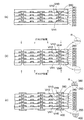
実施形態を説明する前に、基礎となる予備的事項について説明する。コアレスタイプの配線基板の製造方法では、図1(a)に示すように、まず、銅板などの支持体100を用意する。次いで、図1(b)に示すように、支持体100の上に半硬化状態の樹脂フィルムを貼付し、190℃程度の温度で加熱することにより、樹脂フィルムを硬化させて第1樹脂層200を得る。
Prior to describing the embodiment, preliminary items that serve as a basis will be described. In the manufacturing method of the coreless type wiring substrate, as shown in FIG. 1A, first, a
続いて、図1(c)に示すように、第1樹脂層200の上に第1配線層300を形成する。次いで、図1(d)に示すように、第1樹脂層200の形成方法と同様な方法により、第1配線層300を被覆する第2樹脂層220を第1樹脂層200の上に形成する。さらに、第2樹脂層220をレーザなどで加工することにより、第1配線層300に到達する第1ビアホールVH1を形成する。
Subsequently, as shown in FIG. 1C, a
次いで、同じく図1(d)に示すように、第1ビアホールVH1を介して第1配線層300に接続される第2配線層320を第2樹脂層220の上に形成する。
Next, as shown in FIG. 1D, a
続いて、図1(e)に示すように、同様な工程を繰り返すことにより、第3樹脂層240に設けられた第2ビアホールVH2を介して第2配線層320に接続される第3配線層340を第3樹脂層240の上に形成する。
Subsequently, as shown in FIG. 1E, the third wiring layer connected to the
さらに、同様な工程を繰り返すことにより、第4樹脂層260に設けられた第3ビアホールVH3を介して第3配線層340に接続される第4配線層360を第4樹脂層260の上に形成する。その後に、第4配線層360を被覆する第5樹脂層280を形成する。
Further, by repeating the same process, the
このようにして、支持体100の上に4層のビルドアップ配線層を形成する。
In this way, four build-up wiring layers are formed on the
次いで、図2(a)に示すように、ウェットエッチングにより支持体100を除去して、第1樹脂層200の下面を露出させる。
Next, as shown in FIG. 2A, the
続いて、図2(b)に示すように、第5樹脂層280をレーザなどで加工することにより、第4配線層360に到達する第4ビアホールVH4を形成する。さらに、第1樹脂層200をレーザなどで加工することにより、第1配線層300の下面に到達する第5ビアホールVH5を形成する。
Subsequently, as shown in FIG. 2B, the fourth via hole VH4 reaching the
次いで、同じく図2(b)に示すように、両面側において、過マンガン酸カリウム溶液などで第4ビアホールVH4及び第5ビアホールVH5内をデスミア処理することにより、第4、第5ビアホールVH4、VH5の底に残留する樹脂スミアをクリーニングする。 Next, as shown in FIG. 2B, the fourth and fifth via holes VH4 and VH5 are processed by desmearing the inside of the fourth via hole VH4 and the fifth via hole VH5 with a potassium permanganate solution or the like on both sides. Clean any residual resin smear at the bottom of the plate.
このとき同時に、第1樹脂層200及び第5樹脂層280の表面がデスミア処理によってエッチングされる。
At the same time, the surfaces of the
ここで、第1樹脂層200は、第2〜第5樹脂層220,240,260,280を形成するたびに加熱処理が繰り返し施されている。このため、第1樹脂層200は加熱履歴が他の樹脂層より多くなるため、強固に硬化した状態となっている。
Here, the
従って、図2(b)の部分拡大断面図に示すように、デスミア処理を行う際に、第5樹脂層280の表面はエッチングによって十分に凹凸が形成されて所要の粗化面Rとなるが、第1樹脂層200の表面はエッチングされにくいため、十分に粗化されない。
Therefore, as shown in the partial enlarged cross-sectional view of FIG. 2B, when the desmear process is performed, the surface of the
そして、図2(c)に示すように、第4ビアホールVH4を介して第4配線層360に接続される第5配線層380を第5樹脂層280の上に形成する。第5樹脂層280の表面は適度な粗化面Rとなっているため、第5配線層380は密着性よく第5樹脂層280の上に形成される。
Then, as shown in FIG. 2C, a
また、同じく図2(c)に示すように、第5ビアホールVH5を介して第1配線層300に接続される第6配線層400を第1樹脂層200の下面に形成する。第1樹脂層200の下面は十分に粗化されていないため、第6配線層400と第1樹脂層200との十分な密着性が得られない課題がある。
Similarly, as shown in FIG. 2C, a
第6配線層400をセミアディティブ法で形成する場合は、シード層を無電解めっきで形成する際に、シード層が第1樹脂層200から剥がれて膨れが発生しやすい。
When the
このため、第1樹脂層200の下面に形成される第6配線層400は、剥がれ対策のために線幅を太くしたりするなどの工夫が必要になり、他の樹脂層の上に形成される配線層と同じ設計ルールで形成することが困難になり、設計上の制約が生じる。
For this reason, the
以下に説明する実施形態では、前述した不具合を解消することができる。 In the embodiment described below, the above-described problems can be solved.
(実施形態)
図3〜図7は実施形態の配線基板の製造方法を示す断面図、図8は実施形態の配線基板を示す断面図である。以下、実施形態の配線基板の製造方法を説明しながら配線基板の構造について説明する。
(Embodiment)
3 to 7 are cross-sectional views showing a method for manufacturing a wiring board according to the embodiment, and FIG. 8 is a cross-sectional view showing the wiring board according to the embodiment. Hereinafter, the structure of the wiring board will be described while explaining the manufacturing method of the wiring board of the embodiment.
実施形態の配線基板の製造方法では、図3(a)に示すように、まず、支持体10を用意する。支持体10は、例えば、金属板から形成され、一例として、厚みが150μm〜500μmの銅板又は銅箔から形成される。
In the method for manufacturing a wiring board according to the embodiment, as shown in FIG. The
次いで、図3(b)に示すように、支持体10の上に半硬化状態の樹脂フィルムを貼付し、190℃程度の温度で加熱処理することにより、樹脂フィルムを硬化させる。これにより、厚みが20μm程度の第1樹脂層20を得る。樹脂フィルムとしては、熱硬化性のエポキシ樹脂又はポリイミド樹脂などが使用される。その後に、過マンガン酸カリウム溶液などで第1樹脂層20の表面をエッチングして粗化面とする。
Next, as shown in FIG. 3B, a semi-cured resin film is stuck on the
続いて、図3(c)に示すように、第1樹脂層20の上に厚みが20μm程度の第1配線層30を形成する。
Subsequently, as shown in FIG. 3C, a
第1配線層30は、例えば、セミアディティブ法により形成される。詳しく説明すると、図4(a)に示すように、まず、第1樹脂層20の上に無電解めっき又はスパッタ法によって銅などからなるシード層30aを形成する。次いで、図4(b)に示すように、シード層30aの上に、第1配線層30が配置される部分に開口部31xが設けられためっきレジスト31をフォトリソグラフィに基づいて形成する。
The
さらに、図4(c)に示すように、シード層30aをめっき給電経路に利用する電解めっきにより、めっきレジスト31の開口部31xに銅などからなる金属めっき層30bを形成する。
Further, as shown in FIG. 4C, a
次いで、図4(d)に示すように、めっきレジスト31を除去する。その後に、図4(e)に示すように、金属めっき層30bをマスクにしてシード層30aをエッチングして除去する。これにより、シード層30a及び金属めっき層30bから形成される第1配線層30が得られる。
Next, as shown in FIG. 4D, the plating resist 31 is removed. Thereafter, as shown in FIG. 4E, the
続いて、図3(d)に戻って説明すると、第1樹脂層20及び第1配線層30の上に半硬化状態の樹脂フィルムを貼付し、190℃程度の温度で加熱処理することにより、樹脂フィルムを硬化させる。これにより、厚みが30μm程度の第2樹脂層22を得る。第2樹脂層22は層間絶縁層として形成される。後述する第3〜第5樹脂層についても同じである。
Subsequently, returning to FIG. 3 (d), the semi-cured resin film is pasted on the
さらに、第2樹脂層22をレーザなどで加工することにより、第1配線層30に到達する第1ビアホールVH1を形成する。第1ビアホールVH1の直径は、例えば60μm〜70μmに設定される。
Further, the first via hole VH1 reaching the
第1ビアホールVH1は、第2樹脂層22の上面側からレーザなどで形成されるため、第2樹脂層22の表面から厚み方向に向けて直径が小さくなる順テーパー形状で形成される。
Since the first via hole VH1 is formed by a laser or the like from the upper surface side of the
その後に、過マンガン酸カリウム溶液などで第1ビアホールVH1内をデスミア処理することにより、第1ビアホールVH1の底に残留する樹脂スミアをクリーニングする。このとき同時に、図3(d)の部分拡大断面図に示すように、デスミア処理によって、第1ビアホールVH1の側面及び第2樹脂層22の表面に凹凸が形成されて表面が粗化面Rとなる。
Thereafter, the inside of the first via hole VH1 is desmeared with a potassium permanganate solution or the like, thereby cleaning the resin smear remaining at the bottom of the first via hole VH1. At the same time, as shown in the partial enlarged cross-sectional view of FIG. 3D, the desmear treatment forms irregularities on the side surface of the first via hole VH1 and the surface of the
第2樹脂層22の粗化面Rの表面粗さは、500nm以下、好適には100nm〜400nmに設定される。他の樹脂層においても、その表面粗さは第2樹脂層22と同一範囲に設定される。
The surface roughness of the roughened surface R of the
デスミア処理の方法として、過マンガン酸法を例示したが、プラズマエッチング、又はブラスト処理などを使用してもよい。プラズマエッチングを使用する場合は、例えば、CF4にO2又はN2などが添加された混合ガスを使用するドライエッチング装置によって行われる。 Although the permanganic acid method has been exemplified as the desmear treatment method, plasma etching, blast treatment, or the like may be used. In the case of using plasma etching, for example, it is performed by a dry etching apparatus using a mixed gas in which O 2 or N 2 or the like is added to CF 4 .
次いで、図3(e)に示すように、第1ビアホールVH1を介して第1配線層30に接続される第2配線層32を第2樹脂層22の上に形成する。第2樹脂層22の表面は適度に粗化されているため、第2配線層32はアンカー効果によって密着性よく第2樹脂層22の上に形成される。前述した第1配線層30においても、同様な理由で、第1樹脂層20の上に密着性よく形成される。
Next, as illustrated in FIG. 3E, a
第2配線層32は、例えば、セミアディティブ法によって形成される。詳しく説明すると、図5(a)に示すように、まず、第2樹脂層22の上及び第1ビアホールVH1の内面に無電解めっき又はスパッタ法により銅などからなるシード層32aを形成する。
The
さらに、図5(b)に示すように、第2配線層32が配置される部分に開口部31xが設けられためっきレジスト31をシード層32aの上にフォトリソグラフィに基づいて形成する。
Further, as shown in FIG. 5B, a plating resist 31 provided with an
次いで、図5(c)に示すように、シード層32aをめっき給電経路に利用する電解めっきにより、第1ビアホールVH1内からめっきレジスト31の開口部31xに銅などからなる金属めっき層32bを形成する。
Next, as shown in FIG. 5C, a
その後に、図5(d)に示すように、めっきレジスト31を除去した後に、金属めっき層32bをマスクにしてシード層32aをエッチングして除去する。これにより、シード層32a及び金属めっき層32bから形成される第2配線層32が得られる。第2配線層32は第1ビアホールVH1内に充填されたビア導体を含んで形成される。
Thereafter, as shown in FIG. 5D, after the plating resist 31 is removed, the
他の配線層においても、好適には、セミアディティブ法で形成されるが、サブトラクティブ法又はフルアディティブ法などの他の配線形成方法を使用してもよい。 Other wiring layers are preferably formed by a semi-additive method, but other wiring forming methods such as a subtractive method or a full additive method may be used.
次いで、図6(a)に示すように、同様な工程を繰り返すことにより、第3樹脂層24に形成された第2ビアホールVH2を介して第2配線層32に接続される第3配線層34を第3樹脂層24の上に形成する。
Next, as shown in FIG. 6A, by repeating the same process, the
さらに、同様な工程を繰り返すことにより、第4樹脂層26に形成された第3ビアホールVH3を介して第3配線層34に接続される第4配線層36を第4樹脂層26の上に形成する。
Further, by repeating the same process, the
続いて、図6(b)に示すように、支持体10をエッチングによって除去する。支持体10が銅から形成される場合は、支持体10のエッチャントとして、アンモニアを主成分とするアルカリエッチング液、第二塩化鉄水溶液、又は第二塩化銅水溶液などが使用される。これにより、支持体10を第1樹脂層20に対して選択的に除去することができる。
Subsequently, as shown in FIG. 6B, the
前述した予備的事項でも説明したように、最下の第1樹脂層20は、第2〜第4樹脂層22,24,26を形成するたびに加熱処理が繰り返し施されて、加熱履歴が多くなっているため、強固に硬化した状態となっている。このため、最下の第1樹脂層20の露出面に粗化処理を行っても十分な粗化面を得ることは困難である。
As described in the preliminary matter described above, the lowermost
そこで、図6(c)に示すように、第1樹脂層20の下面に密着用樹脂層20aを積層して形成する。密着用樹脂層20aは他の樹脂層と同様に、半硬化状態の樹脂フィルムを貼付し、加熱処理で硬化させることにより得られる。
Therefore, as shown in FIG. 6C, the
また同様に、密着用樹脂層20aは熱硬化性のエポキシ樹脂又はポリイミド樹脂などから形成される。密着用樹脂層20aは過剰な加熱処理が施されていないため、デスミア処理によって容易に粗化面を形成することができる。
Similarly, the
第1樹脂層20及び密着用樹脂層20aによって層間絶縁層が形成される。第1樹脂層20の厚みが20μmの場合は、密着用樹脂層20aの厚みは10μm程度に設定され、トータルの厚みが第2〜第4樹脂層22,24,26の各厚みと同一になるように設定される。
An interlayer insulating layer is formed by the
さらに、同様な方法により、第4樹脂層26及び第4配線層36の上に第5樹脂層28を形成する。
Further, the
次いで、図7(a)に示すように、図6(c)の上面側において、第5樹脂層28をレーザなどで加工することにより、第4配線層36の上面に到達する第4ビアホールVH4を形成する。
Next, as shown in FIG. 7A, the fourth via hole VH4 that reaches the upper surface of the
また同様に、図6(c)の下面側において、密着用樹脂層20a及び第1樹脂層20をレーザなどで加工することにより、第1配線層30の下面に到達する第5ビアホールVH5を形成する。
Similarly, on the lower surface side of FIG. 6C, the
第5ビアホールVH5は、密着用樹脂層20a及び第1樹脂層20の下面側からレーザなどで形成される。このため、第5ビアホールVH5は、密着用樹脂層20aの表面から第1樹脂層20の厚み方向に向けて直径が小さくなる逆テーパー形状で形成され、第1ビアホールVH1とは逆のテーパー形状となる。
The fifth via hole VH5 is formed by a laser or the like from the lower surface side of the
さらに、図7(b)に示すように、図7(a)の構造体の両面側に、過マンガン酸カリウム溶液などでデスミア処理を行うことにより、第4、第5ビアホールVH4,VH5の底に残留する樹脂スミアをクリーニングする。 Further, as shown in FIG. 7B, the bottom surfaces of the fourth and fifth via holes VH4 and VH5 are obtained by performing desmear treatment on both sides of the structure of FIG. 7A with a potassium permanganate solution or the like. Clean any residual resin smear.
このとき同時に、デスミア処理によって、第4、第5ビアホールVH4,VH5の側面及び第5樹脂層28及び密着用樹脂層20aの表面に凹凸が形成されて粗化面となる。
At the same time, by the desmear process, irregularities are formed on the side surfaces of the fourth and fifth via holes VH4, VH5 and the surfaces of the
図7(b)の部分拡大断面図には、密着用樹脂層20aの外面に粗化面Rが形成された様子が示されている。
FIG. 7B is a partially enlarged cross-sectional view showing a state in which the roughened surface R is formed on the outer surface of the
このように、過剰に加熱処理が施されて粗化面の形成が困難な最下の第1樹脂層20の下面に密着用樹脂層20aを形成することにより、第1樹脂層20の下面側に粗化面Rを形成することができる。
Thus, by forming the
これにより、密着用樹脂層20aの外面の表面粗さを第1〜第5樹脂層20,22,24,26,28の各上面の表面粗さと同一範囲に設定することができる。
Thereby, the surface roughness of the outer surface of the
次いで、図7(c)に示すように、図7(b)の構造体の上面側において、第4ビアホールVH4を介して第4配線層36に接続される第5配線層38を第4樹脂層26の上に形成する。
Next, as shown in FIG. 7C, on the upper surface side of the structure of FIG. 7B, the
さらに、同じく図7(c)に示すように、図7(b)の構造体の下面側において、第5ビアホールVH5を介して第1配線層30に接続される第6配線層40を密着用樹脂層20aの外面に形成する。
Further, as shown in FIG. 7C, the
第1樹脂層20の下面には外面が適度に粗化された密着用樹脂層20aが形成されている。このため、最下の第1樹脂層20の下面側に形成される第6配線層40においても、他の配線層と同様に、第1樹脂層20に密着性よく形成される。
On the lower surface of the
前述した第2配線層32の形成方法で説明したセミアディティブ法を使用する場合は、シード層を無電解めっきで形成する際に、シード層が密着用樹脂層20aから剥がれて膨れが発生することなく、歩留りよく微細な第6配線層40を形成することができる。
When the semi-additive method described in the method for forming the
このように、本実施形態の配線基板では、配線層が形成される全ての樹脂層において適度に粗化されているので、全ての層の配線層において十分な密着性が確保される。このため、ビルドアップ配線層の全ての配線層において同じ設計ルールで形成することができ、設計上の制約を生じることがない。 Thus, in the wiring board of this embodiment, since all the resin layers in which the wiring layer is formed are appropriately roughened, sufficient adhesion is secured in all the wiring layers. For this reason, it can form with the same design rule in all the wiring layers of a buildup wiring layer, and the restriction | limiting on a design does not arise.
例えば、全ての層の配線層において、10μm〜30μmの狭ピッチで歩留りよく形成することができる。 For example, all the wiring layers can be formed with a narrow pitch of 10 μm to 30 μm with good yield.
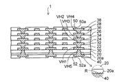
続いて、図8に示すように、最上の第5配線層38の接続部上に開口部50aが設けられたソルダレジスト50を第5樹脂層28の上に形成する。また同様に、最下の第6配線層40の接続部上に開口部52aが設けられたソルダレジスト52を密着用樹脂層20aの上に形成する。
Subsequently, as shown in FIG. 8, a solder resist 50 in which an
さらに、必要に応じて、第5配線層38及び第6配線層40の各接続部にNi/Auめっき層を形成するなどしてコンタクト層(不図示)を設ける。
Furthermore, a contact layer (not shown) is provided by forming a Ni / Au plating layer at each connection portion of the
以上により本実施形態の配線基板1が得られる。
The
前述した形態では、第1樹脂層20の上側に5層のビルドアップ配線層を形成し、第1樹脂層20の下側に1層の配線層を形成したが、第1樹脂層20の上下側において配線層の積層数は任意に設定することができる。
In the above-described embodiment, five build-up wiring layers are formed on the upper side of the
また、層間絶縁層及び密着用絶縁層として絶縁樹脂を使用したが、別の絶縁材料を使用することも可能である。 In addition, although the insulating resin is used as the interlayer insulating layer and the adhesive insulating layer, another insulating material can be used.
図8に示すように、本実施形態の配線基板1では、配線層の間に形成される層間絶縁層の最下層として、第1樹脂層20及び密着用樹脂層20aが配置されている。第1樹脂層20の上に第1配線層30が形成されている。また、第1樹脂層20の上には、第1配線層30に到達する第1ビアホールVH1が設けられた第2樹脂層22が形成されている。
As shown in FIG. 8, in the
さらに、第1ビアホールVH1を介して第1配線層30に接続される第2配線層32が第2樹脂層22の上に形成されている。
Further, a
また同様に、第3樹脂層24に設けられた第2ビアホールVH2を介して第2配線層32に接続される第3配線層34が第3樹脂層24の上に形成されている。
Similarly, a
さらに同様に、第4樹脂層26に設けられた第3ビアホールVH3を介して第3配線層34に接続される第4配線層36が第4樹脂層26の上に形成されている。
Further, similarly, a
さらに同様に、第5樹脂層28に設けられた第4ビアホールVH4を介して第4配線層36に接続される第5配線層38が第5樹脂層28の上に形成されている。第5樹脂層28の上には、第5配線層38の接続部上に開口部50aが設けられたソルダレジスト50が形成されている。
Similarly, a
さらに、密着用樹脂層20a及び第1樹脂層20には、第1配線層30の下面の接続部に到達する第5ビアホールVH5が形成されている。密着用樹脂層20aの下面には、第5ビアホールVH5を介して第1配線層30に接続される第6配線層40が形成されている。第6配線層40の接続部上に開口部52aが設けられたソルダレジスト52が形成されている。
Furthermore, a fifth via hole VH5 reaching the connection portion on the lower surface of the
第6配線層40が形成された密着用樹脂層20aの下面は、部分拡大断面図に示すように、粗化面Rとなっている。密着用樹脂層20aの粗化面Rの表面粗さは、500nm以下、好適には100nm〜400nmの範囲に設定されている。
The lower surface of the
密着用樹脂層20aの下面は適度に粗化されているので、第6配線層40が第1樹脂層20の下面側に密着用樹脂層20aを介して密着性よく形成される。
Since the lower surface of the
また、密着用樹脂層20aの下面の表面粗さは、第1〜第5樹脂層20,22,24,26,28の各上面の表面粗さと同一範囲に設定されている。これにより、第1〜第5配線層30,32,34,36,38の各々においても、密着性よく各樹脂層の上に形成される。
The surface roughness of the lower surface of the
前述したように、コアレスタイプの配線基板の製造方法において、支持体10を除去して露出する最下の第1樹脂層20の露出面を粗化することは困難である。このため、第1樹脂層20の露出面に密着用樹脂層20aを形成する。
As described above, in the method of manufacturing the coreless type wiring substrate, it is difficult to roughen the exposed surface of the lowermost
密着用樹脂層20aは過剰な加熱処理が施されていないため、デスミア処理によって適度に粗化面を形成することができる。
Since the
これにより、第1樹脂層20の露出面側に密着用樹脂層20aを介して第6配線層40を密着性よく形成することができる。
As a result, the
本実施形態の配線基板1では、第2樹脂層22に形成される第1ビアホールVH1は第2樹脂層22の上面側からレーザなどで形成される。このため、第1ビアホールVH1は第2樹脂層22の表面から厚み方向に向けて直径が小さくなる順テーパー形状で形成される。第2〜第4ビアホール(VH2〜VH4)においても同様である。
In the
これに対して、密着用樹脂層20a及び第1樹脂層20に形成される第5ビアホールVH5は密着用樹脂層20aの下面側からレーザなどで形成される。このため、第5ビアホールVH5の形状は、第1ビアホールVH1と逆のテーパー形状で形成される。
In contrast, the fifth via hole VH5 formed in the
図9には、図8の配線基板1を利用した半導体装置の一例が示されている。図9に示すように、半導体装置2では、図8の配線基板1を上下反転させ、第6配線層40の接続部にバンプ電極62を介して半導体チップ60がフリップチップ接続される。
FIG. 9 shows an example of a semiconductor device using the
また、半導体チップ60と配線基板1との隙間にアンダーフィル樹脂64が充填される。さらに、半導体チップ60が搭載された面と反対面側の第5配線層38の接続部に、はんだボールなどを搭載するなどして外部接続端子66を設ける。
In addition, an
そして、半導体装置2の外部接続端子66がマザーボードなどの実装基板に接続される。
Then, the
配線基板1内の配線層によって、半導体チップ60に対応する上面側の第6配線層40の狭ピッチが実装基板の広ピッチに対応するようにピッチ変換される。
Pitch conversion is performed by the wiring layer in the
あるいは、逆に、図8の配線基板1の上面側の第5配線層38の接続部に半導体チップをフリップチップ接続し、反対面側の第6配線層40に外部接続端子を設けてもよい。
Alternatively, conversely, a semiconductor chip may be flip-chip connected to the connection portion of the
1…配線基板、2…半導体装置、10…支持体、20…第1樹脂層、20a…密着用樹脂層、22…第2樹脂層、24…第3樹脂層、26…第4樹脂層、28…第5樹脂層、30…第1配線層、31…めっきレジスト、31x,50a,52a…開口部、32…第2配線層、34…第3配線層、36…第4配線層、38…第5配線層、40…第6配線層、50,52…ソルダレジスト、60…半導体チップ、62…バンプ電極、64…アンダーフィル樹脂、66…外部接続端子、R…粗化面、VH1…第1ビアホール、VH2…第2ビアホール、VH3…第3ビアホール、VH4…第4ビアホール、VH5…第5ビアホール。
DESCRIPTION OF
Claims (9)
前記第1絶縁層の下に形成され、外面が粗化面となった密着用絶縁層と、
前記第1絶縁層の上に形成された第1配線層と、
前記第1絶縁層の上に形成され、前記第1配線層に到達する第1ビアホールが設けられた第2絶縁層と、
前記第2絶縁層の上に形成され、前記第1ビアホールを介して前記第1配線層に接続される第2配線層と、
前記密着用絶縁層及び前記第1絶縁層に形成され、前記第1配線層に到達する第2ビアホールと、
前記密着用絶縁層の外面に形成され、前記第2ビアホールを介して前記第1配線層に接続される第3配線層とを有し、
前記密着用絶縁層の粗化面の表面粗さは、前記第1絶縁層の下面の表面粗さよりも大きく、かつ、
前記密着用絶縁層の粗化面の表面粗さは、前記第1絶縁層及び前記第2絶縁層の各上面の表面粗さと同一範囲に設定されることを特徴とする配線基板。 A first insulating layer;
An insulating layer for adhesion formed under the first insulating layer and having a roughened outer surface;
A first wiring layer formed on the first insulating layer;
A second insulating layer formed on the first insulating layer and provided with a first via hole reaching the first wiring layer;
A second wiring layer formed on the second insulating layer and connected to the first wiring layer through the first via hole;
A second via hole formed in the adhesion insulating layer and the first insulating layer and reaching the first wiring layer;
A third wiring layer formed on the outer surface of the adhesion insulating layer and connected to the first wiring layer through the second via hole;
The surface roughness of the roughened surface of the adhesive insulating layer is much larger than the surface roughness of the lower surface of the first insulating layer, and,
The wiring board according to claim 1, wherein the surface roughness of the roughened surface of the adhesion insulating layer is set in the same range as the surface roughness of each upper surface of the first insulating layer and the second insulating layer .
前記第1絶縁層の上に第1配線層を形成する工程と、
前記第1配線層を被覆する第2絶縁層を前記第1絶縁層の上に形成する工程と、
前記第2絶縁層に、前記第1配線層に到達する第1ビアホールを形成する工程と、
前記第1ビアホールを介して前記第1配線層に接続される第2配線層を前記第2絶縁層の上に形成する工程と、
前記支持体を除去して、前記第1絶縁層の下面を露出させる工程と、
前記第1絶縁層の露出面に密着用絶縁層を形成する工程と、
前記密着用絶縁層及び前記第1絶縁層に、前記第1配線層に到達する第2ビアホールを形成する工程と、
前記密着用絶縁層の露出面を粗化する工程と、
前記第2ビアホールを介して前記第1配線層に接続される第3配線層を前記密着用絶縁層の露出面に形成する工程とを有し、
前記密着用絶縁層の露出面の表面粗さは、前記第1絶縁層及び前記第2絶縁層の各上面の表面粗さと同一範囲に設定されることを特徴とする配線基板の製造方法。 Forming a first insulating layer on the support;
Forming a first wiring layer on the first insulating layer;
Forming a second insulating layer covering the first wiring layer on the first insulating layer;
Forming a first via hole reaching the first wiring layer in the second insulating layer;
Forming a second wiring layer connected to the first wiring layer through the first via hole on the second insulating layer;
Removing the support to expose a lower surface of the first insulating layer;
Forming an adhesion insulating layer on the exposed surface of the first insulating layer;
Forming a second via hole reaching the first wiring layer in the adhesion insulating layer and the first insulating layer;
Roughening the exposed surface of the adhesive insulating layer;
Possess and forming a third wiring layer connected to the first wiring layer through the second via hole to the exposed surface of the adhesive insulating layer,
The method of manufacturing a wiring board , wherein the surface roughness of the exposed surface of the adhesion insulating layer is set in the same range as the surface roughness of each upper surface of the first insulating layer and the second insulating layer .
Priority Applications (2)
| Application Number | Priority Date | Filing Date | Title |
|---|---|---|---|
| JP2012206743A JP6057641B2 (en) | 2012-09-20 | 2012-09-20 | Wiring board and manufacturing method thereof |
| US14/021,110 US9137896B2 (en) | 2012-09-20 | 2013-09-09 | Wiring substrate |
Applications Claiming Priority (1)
| Application Number | Priority Date | Filing Date | Title |
|---|---|---|---|
| JP2012206743A JP6057641B2 (en) | 2012-09-20 | 2012-09-20 | Wiring board and manufacturing method thereof |
Publications (3)
| Publication Number | Publication Date |
|---|---|
| JP2014063801A JP2014063801A (en) | 2014-04-10 |
| JP2014063801A5 JP2014063801A5 (en) | 2015-10-01 |
| JP6057641B2 true JP6057641B2 (en) | 2017-01-11 |
Family
ID=50273291
Family Applications (1)
| Application Number | Title | Priority Date | Filing Date |
|---|---|---|---|
| JP2012206743A Active JP6057641B2 (en) | 2012-09-20 | 2012-09-20 | Wiring board and manufacturing method thereof |
Country Status (2)
| Country | Link |
|---|---|
| US (1) | US9137896B2 (en) |
| JP (1) | JP6057641B2 (en) |
Families Citing this family (5)
| Publication number | Priority date | Publication date | Assignee | Title |
|---|---|---|---|---|
| US9087777B2 (en) * | 2013-03-14 | 2015-07-21 | United Test And Assembly Center Ltd. | Semiconductor packages and methods of packaging semiconductor devices |
| JP6075789B2 (en) * | 2014-01-31 | 2017-02-08 | 京セラ株式会社 | Wiring board manufacturing method |
| JP6550260B2 (en) * | 2015-04-28 | 2019-07-24 | 新光電気工業株式会社 | Wiring board and method of manufacturing wiring board |
| JP7063101B2 (en) * | 2018-05-11 | 2022-05-09 | 住友電気工業株式会社 | Manufacturing method of printed wiring board and printed wiring board |
| KR20230097817A (en) * | 2021-12-24 | 2023-07-03 | 삼성전기주식회사 | Printed circuit board, printed circuit board with carrier and method for manufacturing printed circuit board package |
Family Cites Families (13)
| Publication number | Priority date | Publication date | Assignee | Title |
|---|---|---|---|---|
| DE3913966B4 (en) * | 1988-04-28 | 2005-06-02 | Ibiden Co., Ltd., Ogaki | Adhesive dispersion for electroless plating, and use for producing a printed circuit |
| EP0620703B1 (en) * | 1993-04-12 | 1997-12-29 | Ibiden Co, Ltd. | Resin compositions and printed circuit boards using the same |
| JP4012307B2 (en) | 1998-04-02 | 2007-11-21 | イビデン株式会社 | Manufacturing method of multilayer printed wiring board |
| JP3527694B2 (en) * | 2000-08-11 | 2004-05-17 | 新光電気工業株式会社 | Manufacturing method of wiring board |
| JP2007073834A (en) * | 2005-09-08 | 2007-03-22 | Shinko Electric Ind Co Ltd | Wiring formation method on insulating resin layer |
| KR100881303B1 (en) * | 2005-11-02 | 2009-02-03 | 이비덴 가부시키가이샤 | Multilayer printed wiring board for semiconductor device and process for producing the same |
| US7722950B2 (en) * | 2005-11-14 | 2010-05-25 | World Properties, Inc. | Adhesive compositions for flexible circuit materials, circuits, multi-layer circuits, and methods of manufacture thereof |
| JP4895795B2 (en) | 2006-12-20 | 2012-03-14 | 新光電気工業株式会社 | Manufacturing method of multilayer wiring board |
| JP5092547B2 (en) * | 2007-05-30 | 2012-12-05 | 凸版印刷株式会社 | Method for manufacturing printed wiring board |
| JP5092662B2 (en) | 2007-10-03 | 2012-12-05 | 凸版印刷株式会社 | Method for manufacturing printed wiring board |
| DE112009000839T5 (en) * | 2008-04-10 | 2011-05-12 | World Properties, Inc., Lincolnwood | Improved bond circuit materials, methods of making the same, and articles made therefrom |
| JP5322531B2 (en) * | 2008-05-27 | 2013-10-23 | 新光電気工業株式会社 | Wiring board manufacturing method |
| JP5251464B2 (en) * | 2008-12-03 | 2013-07-31 | 日立化成株式会社 | Insulating resin material for wiring board, multilayer wiring board, and method for manufacturing multilayer wiring board |
-
2012
- 2012-09-20 JP JP2012206743A patent/JP6057641B2/en active Active
-
2013
- 2013-09-09 US US14/021,110 patent/US9137896B2/en active Active
Also Published As
| Publication number | Publication date |
|---|---|
| JP2014063801A (en) | 2014-04-10 |
| US9137896B2 (en) | 2015-09-15 |
| US20140076614A1 (en) | 2014-03-20 |
Similar Documents
| Publication | Publication Date | Title |
|---|---|---|
| JP4564342B2 (en) | Multilayer wiring board and manufacturing method thereof | |
| JP5693977B2 (en) | Wiring board and manufacturing method thereof | |
| TWI670803B (en) | Interposer, semiconductor device, interposer manufacturing method, and semiconductor device manufacturing method | |
| US9763332B2 (en) | Support body, method of manufacturing support body, method of manufacturing wiring board, method of manufacturing electronic component, and wiring structure | |
| JP5258716B2 (en) | Printed circuit board and manufacturing method thereof | |
| JP6208411B2 (en) | Wiring board and manufacturing method thereof | |
| JP2014154800A (en) | Wiring board and manufacturing method thereof | |
| JP6057641B2 (en) | Wiring board and manufacturing method thereof | |
| JP2012216773A (en) | Wiring board and manufacturing method thereof | |
| JP6009300B2 (en) | Wiring board and manufacturing method thereof | |
| JP2011138868A (en) | Multilayer wiring substrate | |
| JP6092555B2 (en) | Wiring board manufacturing method | |
| JP6510884B2 (en) | Wiring board, method of manufacturing the same and electronic component device | |
| JP2006339186A (en) | Wiring board and its manufacturing method | |
| JP2017069524A (en) | Wiring board and manufacturing method of the same | |
| JP4508140B2 (en) | Built-in module | |
| JP5419583B2 (en) | Wiring board manufacturing method | |
| KR100934107B1 (en) | Printed circuit board manufacturing method providing fine pitch metal bumps | |
| TWI635790B (en) | Manufacturing method of wiring substrate | |
| JP5493020B2 (en) | Wiring board manufacturing method and semiconductor package manufacturing method | |
| JP5269757B2 (en) | Multilayer wiring board | |
| TWI496243B (en) | Method for fabricating embedded component semiconductor package | |
| JP2000349438A (en) | Manufacture of semiconductor package | |
| JP2016096245A (en) | Multilayer wiring board manufacturing method | |
| JP2006210769A (en) | Semiconductor element mounting substrate, and its manufacturing method |
Legal Events
| Date | Code | Title | Description |
|---|---|---|---|
| A521 | Request for written amendment filed |
Free format text: JAPANESE INTERMEDIATE CODE: A523 Effective date: 20150812 |
|
| A621 | Written request for application examination |
Free format text: JAPANESE INTERMEDIATE CODE: A621 Effective date: 20150812 |
|
| A977 | Report on retrieval |
Free format text: JAPANESE INTERMEDIATE CODE: A971007 Effective date: 20160518 |
|
| A131 | Notification of reasons for refusal |
Free format text: JAPANESE INTERMEDIATE CODE: A131 Effective date: 20160531 |
|
| A521 | Request for written amendment filed |
Free format text: JAPANESE INTERMEDIATE CODE: A523 Effective date: 20160714 |
|
| TRDD | Decision of grant or rejection written | ||
| A01 | Written decision to grant a patent or to grant a registration (utility model) |
Free format text: JAPANESE INTERMEDIATE CODE: A01 Effective date: 20161122 |
|
| A61 | First payment of annual fees (during grant procedure) |
Free format text: JAPANESE INTERMEDIATE CODE: A61 Effective date: 20161206 |
|
| R150 | Certificate of patent or registration of utility model |
Ref document number: 6057641 Country of ref document: JP Free format text: JAPANESE INTERMEDIATE CODE: R150 |