JP5986397B2 - Inspection jig - Google Patents
Inspection jig Download PDFInfo
- Publication number
- JP5986397B2 JP5986397B2 JP2012041028A JP2012041028A JP5986397B2 JP 5986397 B2 JP5986397 B2 JP 5986397B2 JP 2012041028 A JP2012041028 A JP 2012041028A JP 2012041028 A JP2012041028 A JP 2012041028A JP 5986397 B2 JP5986397 B2 JP 5986397B2
- Authority
- JP
- Japan
- Prior art keywords
- inspection
- wiring
- contact
- electrode
- substrate
- Prior art date
- Legal status (The legal status is an assumption and is not a legal conclusion. Google has not performed a legal analysis and makes no representation as to the accuracy of the status listed.)
- Active
Links
Images
Classifications
-
- G—PHYSICS
- G01—MEASURING; TESTING
- G01R—MEASURING ELECTRIC VARIABLES; MEASURING MAGNETIC VARIABLES
- G01R31/00—Arrangements for testing electric properties; Arrangements for locating electric faults; Arrangements for electrical testing characterised by what is being tested not provided for elsewhere
- G01R31/28—Testing of electronic circuits, e.g. by signal tracer
- G01R31/2851—Testing of integrated circuits [IC]
- G01R31/2886—Features relating to contacting the IC under test, e.g. probe heads; chucks
-
- G—PHYSICS
- G01—MEASURING; TESTING
- G01R—MEASURING ELECTRIC VARIABLES; MEASURING MAGNETIC VARIABLES
- G01R1/00—Details of instruments or arrangements of the types included in groups G01R5/00 - G01R13/00 and G01R31/00
- G01R1/02—General constructional details
- G01R1/06—Measuring leads; Measuring probes
- G01R1/067—Measuring probes
- G01R1/073—Multiple probes
- G01R1/07307—Multiple probes with individual probe elements, e.g. needles, cantilever beams or bump contacts, fixed in relation to each other, e.g. bed of nails fixture or probe card
- G01R1/07314—Multiple probes with individual probe elements, e.g. needles, cantilever beams or bump contacts, fixed in relation to each other, e.g. bed of nails fixture or probe card the body of the probe being perpendicular to test object, e.g. bed of nails or probe with bump contacts on a rigid support
- G01R1/07328—Multiple probes with individual probe elements, e.g. needles, cantilever beams or bump contacts, fixed in relation to each other, e.g. bed of nails fixture or probe card the body of the probe being perpendicular to test object, e.g. bed of nails or probe with bump contacts on a rigid support for testing printed circuit boards
-
- G—PHYSICS
- G01—MEASURING; TESTING
- G01R—MEASURING ELECTRIC VARIABLES; MEASURING MAGNETIC VARIABLES
- G01R31/00—Arrangements for testing electric properties; Arrangements for locating electric faults; Arrangements for electrical testing characterised by what is being tested not provided for elsewhere
- G01R31/28—Testing of electronic circuits, e.g. by signal tracer
- G01R31/2851—Testing of integrated circuits [IC]
- G01R31/2853—Electrical testing of internal connections or -isolation, e.g. latch-up or chip-to-lead connections
-
- H—ELECTRICITY
- H05—ELECTRIC TECHNIQUES NOT OTHERWISE PROVIDED FOR
- H05K—PRINTED CIRCUITS; CASINGS OR CONSTRUCTIONAL DETAILS OF ELECTRIC APPARATUS; MANUFACTURE OF ASSEMBLAGES OF ELECTRICAL COMPONENTS
- H05K1/00—Printed circuits
- H05K1/02—Details
- H05K1/0266—Marks, test patterns or identification means
- H05K1/0268—Marks, test patterns or identification means for electrical inspection or testing
Landscapes
- Engineering & Computer Science (AREA)
- Microelectronics & Electronic Packaging (AREA)
- Physics & Mathematics (AREA)
- General Physics & Mathematics (AREA)
- Computer Hardware Design (AREA)
- General Engineering & Computer Science (AREA)
- Measuring Leads Or Probes (AREA)
- Tests Of Electronic Circuits (AREA)
- Testing Electric Properties And Detecting Electric Faults (AREA)
- Testing Of Short-Circuits, Discontinuities, Leakage, Or Incorrect Line Connections (AREA)
- Production Of Multi-Layered Print Wiring Board (AREA)
Description
本発明は、配線パターンが形成されるとともに電子部品が内蔵される基板と、この基板を検査する基板検査装置とを電気的に接続する検査用治具に関し、より詳しくは、基板に内蔵される電子部品の過電圧による破壊を防止する検査用治具に関する。 The present invention relates to an inspection jig for electrically connecting a substrate on which a wiring pattern is formed and an electronic component is embedded, and a substrate inspection apparatus for inspecting the substrate, and more specifically, is incorporated in the substrate. The present invention relates to an inspection jig for preventing destruction of electronic components due to overvoltage.
現在、コンデンサ及び抵抗等の電子部品を内蔵した部品内蔵基板(エンベデッド基板とも言われる)の普及が始まりつつあり、部品内蔵基板内に内蔵された電子部品に対する検査方法の確立が早急に求められている。部品内蔵基板自体が新しいものであるため、その検査方法についても従来技術と呼べるような既存の技術が存在しないのが実状である。そこで、部品内蔵基板についての検査方法について開示のある先行文献として、例えば、特許文献1を例示することができる。 Currently, the spread of component-embedded boards (also called embedded boards) with built-in electronic components such as capacitors and resistors is beginning to spread, and there is an urgent need to establish an inspection method for electronic components built into the component-embedded boards. Yes. Since the component-embedded substrate itself is new, there is no existing technology that can be called a conventional technology for the inspection method. Thus, for example, Patent Document 1 can be exemplified as a prior art document that discloses an inspection method for a component built-in substrate.
この特許文献1に開示される先行技術文献では、部品内蔵基板を検査する場合であっても、低コストで且つ短時間で部品内蔵基板の検査を実施することを目的として、4つの周波数の検査信号を用いる基板検査装置を設けることによって、検査を実現している。 In the prior art document disclosed in this Patent Document 1, even when inspecting a component-embedded substrate, the inspection of four frequencies is performed for the purpose of performing the inspection of the component-embedded substrate at a low cost and in a short time. Inspection is realized by providing a substrate inspection device using a signal.
このような基板検査方法では、通常、基板へ検査を実施するための入力信号を供給することができるとともに、この入力信号に応じた出力信号を受信して、この出力信号を基に、基板の良品/不良品を判定することができる基板検査装置が用いられる。また、この基板検査装置と検査対象の基板を電気的に接続するための検査用治具が用いられることになる。また、このような基板検査装置は、基板に応じてカスタマイズされるものではなく、上記の如き電気信号の入出力や信号処理ができる汎用的な機能を有するのみであり、検査用治具が基板の種類に応じてカスタマイズされて用いられることになる。なお、実際の検査では、基板検査装置に検査手順や検査条件が記憶されており、この記憶された手順や条件に従って、検査が実行されることになる。 In such a substrate inspection method, an input signal for performing an inspection can be normally supplied to the substrate, an output signal corresponding to the input signal is received, and the substrate is checked based on the output signal. A substrate inspection apparatus capable of determining good / defective products is used. In addition, an inspection jig for electrically connecting the substrate inspection apparatus and the substrate to be inspected is used. Further, such a substrate inspection apparatus is not customized according to the substrate, but has only a general function capable of inputting / outputting electric signals and processing signals as described above, and the inspection jig is the substrate. It will be customized and used according to the type. In the actual inspection, the inspection procedure and the inspection conditions are stored in the substrate inspection apparatus, and the inspection is executed according to the stored procedures and conditions.
しかしながら、上記の如き従前の検査方法では、部品内蔵基板のように電子部品が内蔵される基板を検査する場合には、電子部品を破壊しないように予め電子部品が接続される配線に応じた検査電圧が設定されている。このため、電子部品が配置される配線と、電子部品が配置されない配線とでは、検査電圧が相違していることになる。
このような場合に、基板検査装置に記憶される検査条件が間違って記憶されていたとすると、基板の検査が実行される毎に電子部品が破壊されるという問題を有している。
However, in the conventional inspection method as described above, when inspecting a substrate in which an electronic component is embedded, such as a component-embedded substrate, an inspection corresponding to a wiring to which the electronic component is connected in advance so as not to destroy the electronic component. The voltage is set. For this reason, the inspection voltage is different between the wiring in which the electronic component is arranged and the wiring in which the electronic component is not arranged.
In such a case, if the inspection condition stored in the board inspection apparatus is stored in error, there is a problem that the electronic component is destroyed every time the inspection of the board is executed.
本発明は、このような実情に鑑みてなされたもので、電子部品が内蔵される基板を検査する場合に、基板検査装置に設定される検査条件等に影響されることなく、基板に内蔵される電子部品の過電圧による破壊を防止する検査用治具を提供する。 The present invention has been made in view of such circumstances, and when inspecting a substrate in which an electronic component is embedded, it is embedded in the substrate without being affected by the inspection conditions set in the substrate inspection apparatus. An inspection jig for preventing destruction of an electronic component due to overvoltage is provided.
請求項1記載の発明は、電子部品を内蔵する部品内蔵基板に形成される配線の電気的な検査を行う基板検査装置と、該部品内蔵基板を電気的に接続するための検査用治具であって、前記基板の配線上に設定される複数の検査点に一方端が当接されるとともに電気的に接続される複数の棒状の接触子と、前記接触子の他方端と当接するとともに電気的に接続される電極部を複数有する電極体と、前記複数の接触子の一方端を夫々の所定の検査点に案内し、他方端を夫々の所定の電極部へ案内する保持体と、前記複数の電極部と電気的に夫々接続される複数の配線部と、前記配線部の他端と電気的に接続されるとともに前記基板検査装置と電気的に接続される接続部を複数有する接続体を有し、前記複数の接触子は、前記電子部品を含む配線の一端が検査点と当接する第一の接触子と、該配線の他端が検査点と当接する第二の接触子と、を含み、前記第一の接触子に前記電極部を介して電気的に接続される前記配線部と、前記第二の接触子に前記電極部を介して電気的に接続される前記配線部とが、電圧クランプ部により電気的に接続されることを特徴とする検査用治具を提供する。
請求項2記載の発明は、前記検査用治具は、前記電圧クランプ部と前記保持体が配置される土台部を有することを特徴とする請求項1記載の検査用治具ることを特徴とする請求項1記載の検査用治具を提供する。
請求項3記載の発明は、前記電圧クランプ部は、定電圧ダイオードであることを特徴とする請求項1又は2に記載の検査用治具を提供する。
これらの発明を提供することによって、上記課題を悉く解決する。
The invention according to claim 1 is a substrate inspection apparatus for performing an electrical inspection of wiring formed on a component built-in substrate in which an electronic component is embedded, and an inspection jig for electrically connecting the component built-in substrate. A plurality of rod-shaped contacts that are in contact with and electrically connected to a plurality of inspection points set on the wiring of the substrate; and a contact that is in contact with the other end of the contacts and An electrode body having a plurality of electrode parts connected to each other, a holding body for guiding one end of each of the plurality of contacts to each predetermined inspection point, and the other end to each predetermined electrode part, A connection body having a plurality of wiring portions electrically connected to the plurality of electrode portions, and a plurality of connection portions electrically connected to the other end of the wiring portion and electrically connected to the substrate inspection apparatus have the plurality of contacts are, the wiring including the electronic component one Includes a first contact that makes contact with the inspection point, and a second contact that makes the other end of the wiring contact with the inspection point, and is electrically connected to the first contact through the electrode portion. examination and the wiring portion to be connected, and said wiring portion electrically connected through the electrode portion to the second contact, characterized that you are electrically connected by the voltage clamp unit Provide jigs.
According to a second aspect of the invention, the inspection jig, the test Chiguru of claim 1, wherein Rukoto which having a base portion to which the holding member and the voltage clamp portion is arranged An inspection jig according to claim 1 is provided.
A third aspect of the present invention provides the inspection jig according to the first or second aspect, wherein the voltage clamp portion is a constant voltage diode.
By providing these inventions, the above problems can be solved.
請求項1記載の発明によれば、電子部品を含んだ配線の一端と他端とに夫々接触する接触子間を所定電圧に制御する電圧クランプ部が設けられるので、電子部品に印加される検査電圧を一定にすることができる。このため、電子部品に対して必要以上の電圧が印加されることがないため、電子部品が破壊されることがない。また、このような電子部品を過電圧による破壊を予防するための電圧クランプ部が検査用治具に設けられるため、基板検査装置から供給される検査信号が電子部品にとって過電圧となる検査信号であっても、電子部品が破壊されることがなく、電圧クランプ部が所定の接触子と接続する配線部間で接続されているため、検査用治具を容易に製造することができる。
請求項2記載の発明によれば、土台部によって検査用治具の強度を保つことができる。
請求項3記載の発明によれば、電圧クランプ部が定電圧ダイオードであるため、簡便に検査用治具を製造することができる。
According to the first aspect of the present invention, since the voltage clamp part for controlling the contact between the one end and the other end of the wiring including the electronic component to a predetermined voltage is provided, the inspection applied to the electronic component The voltage can be kept constant. For this reason, since the voltage beyond necessity is not applied with respect to an electronic component, an electronic component is not destroyed. In addition, since the inspection jig is provided with a voltage clamp portion for preventing such electronic components from being destroyed by overvoltage, the inspection signal supplied from the substrate inspection apparatus is an inspection signal that is overvoltage for the electronic component. also, rather greens that the electronic components are destroyed, since the voltage clamp portion is connected between the wiring portion to be connected to predetermined contacts, it is possible to easily manufacture the inspection jig.
According to the second aspect of the present invention, the strength of the inspection jig can be maintained by the base portion.
According to the invention described in claim 3, since the voltage clamp portion is a constant voltage diode, the inspection jig can be easily manufactured.
本発明を実施するための最良の形態を説明する。
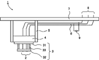
図1は、本発明に係る検査用治具1の一実施形態の概略の構成を示す側面図である。図1では、図面の簡略化の為に三本の接触子2を示しているが、これらは三本に限られず、検査対象に設定される検査点に応じて本数が決定される。
検査用治具1は、複数の接触子2と、これら複数の接触子2を保持する保持体3と、複数の電極部41を有する電極体4と、電極体4を支持する支柱部5と、電極部41から延設されて基板検査装置(図示せず)と電極部41を電気的に接続する配線部6と、複数の接触子2や保持体3や接続体4や支柱部5などの土台となる土台部7と、基板検査装置と導線部6を接続する接続体8を有してなる。
The best mode for carrying out the present invention will be described.
FIG. 1 is a side view showing a schematic configuration of an embodiment of an inspection jig 1 according to the present invention. In FIG. 1, three
The inspection jig 1 includes a plurality of
接触子2は、一端が検査対象物の基板上に設定される所定の検査点と当接して導通接続され、他端が後述する電極部41に当接して導通接続される。この接触子2は、所定の長さを有する細長い棒状形状を有している。
接触子2は、可撓性を有する導電性を有する素材にて形成されている。接触子2は、両端部を除く全周に亘って絶縁被覆が形成され、絶縁被膜による段差を利用して、保持体3に装着されることになる。また、接触子2は可撓性を有しており、保持体3に装着される際には、僅かに一定方向に湾曲して装着される。このように接触子2が湾曲して装着されることによって、復元力により、電極部41と検査点に押圧する押圧力が生じることになる。
One end of the
The
この接触子2の具体的な素材としては、例えば、タングステン、ベリリウム銅やニッケル若しくはそれらの合金などを用いることができる。また、絶縁被覆の素材として、ウレタンやフッ素化樹脂(ポリプロピレン(polypropylene)やポリテトラフルオロエチレン(PTFE))などを用いることができる。
接触子2の検査点に当接する先端の形状は、鋭形状に形成されるが、特に限定されるものではなく、例えば、平坦形状、王冠形状、円錐形状や円筒形状に形成することができる。
As a specific material of the
The shape of the tip that contacts the inspection point of the
保持体3は、複数の接触子2の一方端を夫々の所定の検査点に案内し、他方端を夫々の所定の電極部41へ案内する。保持体3は、図1で示される如く、所定空間を有して配置される電極側板部31と検査側板部32の二つの部材により形成することができる。なお、この電極側板部31と検査側板部32の間の空間は、接触子2が湾曲する空間となる。
The holding body 3 guides one end of each of the plurality of
電極側板部31は、絶縁素材から形成されており、接触子2の他方端を電極部41へ案内するための案内孔(図示せず)が形成されている。電極側板部31は、一枚又は複数枚の板状部材から形成することができる。電極側板部31は、後述する電極体4と当接して配置される。このように配置されることによって、接触子2の他方端を電極部41へ案内し易くしている。
The electrode
検査側板部32は、絶縁素材から形成されており、接触子2の一方端を検査点へ案内するための案内孔(図示せず)が形成されている。検査側板部32は、一枚又は複数枚の板状部材から形成することができる。検査側板部32の案内孔からは、接触子2が突出している状態となる。このような状態になることにより、基板の検査点と接触子2の先端が当接することができる。
The inspection
電極側板部31と検査側板部32は、上記の如き空間を形成するために、所定数の支柱33により支持される。この支柱33の長さによって、接触子2が湾曲する空間が形成されることになる。
The electrode
電極体4は、複数の接触子2の他方端と夫々導通接触する複数の電極部と、これら電極部を保持する絶縁素材から形成される電極保持部を有している。電極部は、電極体4の表面の所定の位置に配置されるように形成され、電極体4の裏面から後述する配線部6と接続されている。
電極部は、電極体4の表面にて、接触子2の外径と同じか僅かに大きい径を有する円形になるよう形成される。電極部の表面は、金めっきされることが好ましい。電極部の一端は、上記の如き接触子2と当接する部位となり、他端は配線部6と接続されることになる。
尚、導線部6は土台部7の裏側面から突出するように配置される接続体8の接続部(図示せず)に接続されており、接続体8が裏面側に配置され、基板検査装置と電気的に接続することができるように配置されている。
The electrode body 4 includes a plurality of electrode portions that are in conductive contact with the other ends of the plurality of
The electrode portion is formed on the surface of the electrode body 4 so as to have a circular shape having a diameter that is the same as or slightly larger than the outer diameter of the
In addition, the
電極保持部は、電極部を保持するための絶縁素材にて板形状に形成されており、この電極保持部には電極部を保持するための貫通孔(図示せず)が形成されている。 The electrode holding part is formed into a plate shape with an insulating material for holding the electrode part, and a through hole (not shown) for holding the electrode part is formed in the electrode holding part.
配線部6は、一端側が複数の電極部と電気的に接続されるとともに、後端が後述する接続部と電気的に接続される。この配線部6は、絶縁被覆された銅(Cu)の線材等の所謂導線を採用することができる。
なお、電極部と配線部6は、一体形成することができる。例えば、所定の長さを有する導線を準備する。電極保持部に形成される貫通孔に、この導線を貫通配置させる。次いで、電極保持部の表面と導線が面一となるように、導線を切断する。電極保持部の表面には、導線の切断面が形成され、この切断面を電極部として利用することができる。このように形成することで、電極部と配線部6を一体的に形成することができる。なお、この導線の切断面に金めっきを行うことになる。
The
The electrode part and the
支柱部5は、電極体4(及び保持体3と接触子2)を支持する(図1参照)。この図1の実施形態では、電極体4の四隅に夫々支柱部5が形成され、電極体4を支える構造を有している。
尚、支柱部5の長さは、検査用治具1の高さを調整することになるが、その高さは検査装置の大きさに応じて適宜変更される。
The support |
In addition, although the length of the support |
土台部7は、複数の接触子2や保持体3や接続体4や支柱部5などの土台として形成される。この土台部7は基板検査装置に応じてその形状や寸法が決定されるが、例えば、板形状に形成される。この土台部7が、基板検査装置に装着するためのガイドの役割を果たすととともに、検査用治具1の強度を保つことになる。
The
接続体8は、導線部6の他端に接続されるとともに、基板検査装置と電気的に接続することを可能にする。この接続体8は、土台部7の裏面側(電極体4、保持体3や接触子2が設けられる側と反対側)に設けられている。この接続体8は、夫々の配線部6と接続される接続部を複数備えてなり、これら夫々の接続部が、基板検査装置と接続されることになる。
この接続部として、裏面側に突出する雄型のピン構造や雌型のコネクタ構造を採用することができる。この接続部の構造は、基板検査装置側の接続端子の構造に応じて決定されることになる。
The
As this connection portion, a male pin structure or a female connector structure protruding on the back surface side can be adopted. The structure of the connection portion is determined according to the structure of the connection terminal on the board inspection apparatus side.
電圧クランプ部9は、電子部品を含む配線の一端が検査点と設定される接触子2と、配線の他端が検査点と設定される接触子2とに印加される検査時の電圧が、所定の電圧となるように調整する。この電圧クランプ部9は、電子部品を含む配線の両端に印加される検査電圧が、電子部品の耐電圧を超えないように設定される。
The
この電圧クランプ部9は、電子部品を含む配線の一端が検査点として設定される接触子2と電気的に接続される配線部6と、電子部品を含む配線の他端の検査点として設定される接触子2と電気的に接続される配線部6とが電気的に接続される。このように電圧クランプ部9が所定の配線部6同士を接続することによって、電圧クランプ部9を容易に検査用治具1に備え付けることができる。
The
電圧クランプ部9は、上記の如き機能を有していれば特に限定されるものではないが、例えば、定電圧ダイオードを用いることができる。この定電圧ダイオードを用いることによって、簡便に製造することができる。
Although the
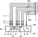
次に、配線部6間を電気的接続する電圧クランプ部9の設定される方法について説明する。図2は、電圧クランプ部9が用いられる状態を示す概略図である。なお、図2での基板は、基板に形成される配線の状態を理解するために、基板の断面を示している。図2で示される基板CBは、本発明の解説のために示されたものであり、このような基板CBは一実施形態に過ぎない。この検査対象となる基板CBには、検査対象となる配線が6本形成されている。この6本の検査対象の配線wには、基板CBの表面CBfから裏面CBrへ接続するように形成される配線w1と、配線w5と配線w6があり、基板CBの表面CBfから表面CBfへ接続するように形成される配線w2、配線w3と配線w4がある。また、配線w3と配線w4は、電子部品ed1と電子部品ed2を含んでいる。
Next, a method of setting the
検査用治具1は、基板CBの表面CBfに当接する治具と裏面CBrに当接する治具と二つ作成することができるが、図2では基板CBの表面CBf用の治具を模式的に示している。また、説明の都合上、夫々のラインにa乃至iの符号を付けて説明する。例えば、配線w1を検査するための検査点を検査点a、配線w2を検査するための検査点を検査点bと検査点e、配線w3を検査するための検査点を検査点cと検査点dとする。また、検査点aに当接する接触子を接触子2aとし、接触子2aと当接する電極部を電極部41aとする。また、電極部41aは配線部6aと接続されており、配線部6aは接続部8aと接続されている。 Two inspection jigs 1 can be prepared: a jig that abuts on the front surface CBf of the substrate CB and a jig that abuts on the back surface CBr. FIG. 2 schematically shows a jig for the front surface CBf of the substrate CB. It shows. For convenience of explanation, each line will be described with a through i symbols. For example, the inspection point for inspecting the wiring w1 is the inspection point a, the inspection point for inspecting the wiring w2 is the inspection point b and the inspection point e, and the inspection point for inspecting the wiring w3 is the inspection point c and the inspection point. Let d. Further, a contact that contacts the inspection point a is referred to as a contact 2a, and an electrode that contacts the contact 2a is referred to as an electrode 41a. The electrode part 41a is connected to the wiring part 6a, and the wiring part 6a is connected to the connection part 8a.
この基板CBを検査する場合には、配線wを検査するために設定される検査点に接触子2が夫々配置される。次に、配線w3と配線w4には、電子部品ed1と電子部品ed2が夫々配置されており、基板検査装置からの検査電圧が過電圧の場合には、電子部品ed1と電子部品ed2が破壊されることになる。このため、配線w3の検査点cに接続される接触子2cと、配線w3の検査点dに接続される接触子2dとには、電子部品ed1の定格電圧を考慮した検査電圧が印加されるよう設定される。具体的には、接触子2cと接続される配線部6cと接触子2dと接続される配線部6dとの間に電圧クランプ部91が接続される。
When inspecting the substrate CB, the
この電圧クランプ部91は、定電圧ダイオードを用いることでき、この検査点間(検査点cと検査点d)に所定電圧以上が印加されないように、定電圧ダイオードの一端と配線部6cが接続され、定電圧ダイオードの他端と配線部6dが接続されることになる。
The
また、電子部品ed2も、電子部品ed1と同様に、検査点gと検査点hとの間に過電圧が印加されないように、電圧クランプ部92が接続される。この電圧クランプ部92は、配線部6gと配線部6hと接続される。具体的には、定電圧ダイオードの一端と配線部6gが接続され、定電圧ダイオードの他端と配線部6hが接続されることになる。
Similarly to the electronic component ed1, the electronic component ed2 is connected to the
検査用治具は、基板CBに合わせて製造されるものであるため、検査用治具に電圧クランプ部を設けることによって、その基板に内蔵される電子部品に応じた過電圧防止(保護回路)手段を設けることができることになり、基板を検査中の過電圧破壊から保護することができる。
以上が本発明の検査用治具の説明である。
Since the inspection jig is manufactured according to the substrate CB, an overvoltage prevention (protection circuit) means corresponding to the electronic component built in the substrate is provided by providing a voltage clamp portion on the inspection jig. The substrate can be protected from overvoltage breakdown during inspection.
The above is the description of the inspection jig of the present invention.
1・・・検査用治具 2・・・接触子 3・・・保持体 4・・・電極体 6・・・配線部 8・・・接続体 9・・・電圧クランプ部
DESCRIPTION OF SYMBOLS 1 ...
Claims (3)
前記基板の配線上に設定される複数の検査点に一方端が当接されるとともに電気的に接続される複数の棒状の接触子と、
前記接触子の他方端と当接するとともに電気的に接続される電極部を複数有する電極体と、
前記複数の接触子の一方端を夫々の所定の検査点に案内し、他方端を夫々の所定の電極部へ案内する保持体と、
前記複数の電極部と電気的に夫々接続される複数の配線部と、
前記配線部の他端と電気的に接続されるとともに前記基板検査装置と電気的に接続される接続部を複数有する接続体を有し、
前記複数の接触子は、
前記電子部品を含む配線の一端が検査点と当接する第一の接触子と、
該配線の他端が検査点と当接する第二の接触子と、
を含み、
前記第一の接触子に前記電極部を介して電気的に接続される前記配線部と、前記第二の接触子に前記電極部を介して電気的に接続される前記配線部とが、電圧クランプ部により電気的に接続されることを特徴とする検査用治具。 A board inspection apparatus for performing electrical inspection of wiring formed on a component-embedded substrate containing electronic components, and an inspection jig for electrically connecting the component-embedded substrate,
A plurality of bar-shaped contacts that are electrically connected to one end of a plurality of inspection points set on the wiring of the substrate;
An electrode body having a plurality of electrode portions that are in contact with and electrically connected to the other end of the contact;
A holding body for guiding one end of each of the plurality of contacts to each predetermined inspection point and guiding the other end to each predetermined electrode portion;
A plurality of wiring portions electrically connected to the plurality of electrode portions, respectively;
A connection body having a plurality of connection portions electrically connected to the other end of the wiring portion and electrically connected to the substrate inspection apparatus;
The plurality of contacts are
A first contact with which one end of the wiring including the electronic component comes into contact with the inspection point;
A second contact where the other end of the wiring contacts the inspection point;
Including
The wiring part electrically connected to the first contact through the electrode part and the wiring part electrically connected to the second contact through the electrode part are voltage inspection jig characterized that you are electrically connected by the clamp portion.
The inspection jig according to claim 1, wherein the voltage clamp unit is a constant voltage diode.
Priority Applications (4)
| Application Number | Priority Date | Filing Date | Title |
|---|---|---|---|
| JP2012041028A JP5986397B2 (en) | 2012-02-28 | 2012-02-28 | Inspection jig |
| KR1020130009624A KR101983732B1 (en) | 2012-02-28 | 2013-01-29 | Inspection jig |
| TW102106789A TWI579574B (en) | 2012-02-28 | 2013-02-26 | Inspection jig |
| CN201310061110.4A CN103293345B (en) | 2012-02-28 | 2013-02-27 | Inspection fixture |
Applications Claiming Priority (1)
| Application Number | Priority Date | Filing Date | Title |
|---|---|---|---|
| JP2012041028A JP5986397B2 (en) | 2012-02-28 | 2012-02-28 | Inspection jig |
Publications (2)
| Publication Number | Publication Date |
|---|---|
| JP2013178108A JP2013178108A (en) | 2013-09-09 |
| JP5986397B2 true JP5986397B2 (en) | 2016-09-06 |
Family
ID=49094567
Family Applications (1)
| Application Number | Title | Priority Date | Filing Date |
|---|---|---|---|
| JP2012041028A Active JP5986397B2 (en) | 2012-02-28 | 2012-02-28 | Inspection jig |
Country Status (3)
| Country | Link |
|---|---|
| JP (1) | JP5986397B2 (en) |
| KR (1) | KR101983732B1 (en) |
| TW (1) | TWI579574B (en) |
Families Citing this family (2)
| Publication number | Priority date | Publication date | Assignee | Title |
|---|---|---|---|---|
| CN105954549A (en) * | 2016-05-11 | 2016-09-21 | 国家电网公司 | Multifunctional multimeter meter pen |
| JP7008529B2 (en) * | 2018-02-15 | 2022-01-25 | 東京特殊電線株式会社 | Lead wires for inspection equipment, lead wire mounting parts, and inspection jigs |
Family Cites Families (10)
| Publication number | Priority date | Publication date | Assignee | Title |
|---|---|---|---|---|
| JPS61144481U (en) * | 1985-02-28 | 1986-09-06 | ||
| JPS6291869A (en) * | 1985-10-18 | 1987-04-27 | Atetsuku Kk | Reverse insertion detecting method for ic parts |
| EP0496147A1 (en) * | 1991-01-25 | 1992-07-29 | John Fluke Mfg. Co., Inc. | Method of precise measurement of small resistance values |
| JPH0658373U (en) * | 1993-01-25 | 1994-08-12 | スタック電子株式会社 | Probe with FET amplifier protection circuit |
| JP2001133483A (en) * | 1999-11-04 | 2001-05-18 | Takashi Nansai | Jig for w-stroke printed board inspecting machine |
| JP4041831B2 (en) * | 2006-05-15 | 2008-02-06 | 日本電産リード株式会社 | Substrate inspection jig and electrode structure of connection electrode portion in this jig |
| JP2007309814A (en) | 2006-05-19 | 2007-11-29 | Hioki Ee Corp | Board inspection equipment |
| JP5028658B2 (en) * | 2006-12-01 | 2012-09-19 | ネッツエスアイ東洋株式会社 | Probing adapter and probe apparatus using the same |
| JP2010197267A (en) * | 2009-02-26 | 2010-09-09 | Tsutomu Takahashi | Electronic circuit board inspection device and inspection tool |
| KR101112621B1 (en) * | 2010-03-05 | 2012-02-16 | 삼성전기주식회사 | Abnormality judgment method for printed circuit board having passive component therein |
-
2012
- 2012-02-28 JP JP2012041028A patent/JP5986397B2/en active Active
-
2013
- 2013-01-29 KR KR1020130009624A patent/KR101983732B1/en active Active
- 2013-02-26 TW TW102106789A patent/TWI579574B/en active
Also Published As
| Publication number | Publication date |
|---|---|
| CN103293345A (en) | 2013-09-11 |
| TWI579574B (en) | 2017-04-21 |
| KR101983732B1 (en) | 2019-05-29 |
| JP2013178108A (en) | 2013-09-09 |
| TW201335608A (en) | 2013-09-01 |
| KR20130098901A (en) | 2013-09-05 |
Similar Documents
| Publication | Publication Date | Title |
|---|---|---|
| US9291645B2 (en) | Probe unit | |
| JP5607934B2 (en) | Probe unit | |
| JP2014235112A (en) | Substrate inspection method, substrate inspection device, and substrate inspection jig | |
| JPH1164425A (en) | Method and device for continuity inspection in electronic part | |
| JP6283929B2 (en) | Inspection jig and method for manufacturing inspection jig | |
| CN210142148U (en) | Test fixture for observing current through a set of resistors | |
| JP5986397B2 (en) | Inspection jig | |
| JP2007178163A (en) | Inspection unit and outer sheath tube assembly for inspection probe used for it | |
| WO2014188701A1 (en) | Board inspection method | |
| JP4064091B2 (en) | Manufacturing method of electrical connector | |
| JP6381439B2 (en) | Cable connection structure | |
| JP5228610B2 (en) | PCB inspection jig | |
| JP2009047636A (en) | Conduction inspection tool of printed circuit board | |
| CN103293345B (en) | Inspection fixture | |
| JP2010276359A (en) | Inspection jig for board inspection device | |
| JP2013002976A (en) | Probe unit, circuit board inspection device and probe unit manufacturing method | |
| JP2011137664A (en) | Inspection jig | |
| JP5185310B2 (en) | Electrical connection body and manufacturing method thereof | |
| JP2012182143A (en) | Mounting structure for high-frequency coaxial connector, and connection method for high-frequency coaxial connector | |
| WO2025258464A1 (en) | Measurement jig and measurement device used in electric characteristic measurement | |
| TW202503279A (en) | Electrical contactor and method of manufacturing electrical contactor | |
| JPH06260799A (en) | Circuit board inspecting method, and circuit board | |
| KR200475381Y1 (en) | The pin for printedcircuit board inspection fixture and printedcircuit board inspection fixture thereof | |
| JP3185893U (en) | Electrode parts for measuring electronic circuits | |
| JP2010025665A (en) | Substrate inspection jig and contact |
Legal Events
| Date | Code | Title | Description |
|---|---|---|---|
| A621 | Written request for application examination |
Free format text: JAPANESE INTERMEDIATE CODE: A621 Effective date: 20150128 |
|
| A977 | Report on retrieval |
Free format text: JAPANESE INTERMEDIATE CODE: A971007 Effective date: 20151203 |
|
| A131 | Notification of reasons for refusal |
Free format text: JAPANESE INTERMEDIATE CODE: A131 Effective date: 20151215 |
|
| A521 | Request for written amendment filed |
Free format text: JAPANESE INTERMEDIATE CODE: A523 Effective date: 20160212 |
|
| TRDD | Decision of grant or rejection written | ||
| A01 | Written decision to grant a patent or to grant a registration (utility model) |
Free format text: JAPANESE INTERMEDIATE CODE: A01 Effective date: 20160705 |
|
| A61 | First payment of annual fees (during grant procedure) |
Free format text: JAPANESE INTERMEDIATE CODE: A61 Effective date: 20160805 |
|
| R150 | Certificate of patent or registration of utility model |
Ref document number: 5986397 Country of ref document: JP Free format text: JAPANESE INTERMEDIATE CODE: R150 |
|
| R250 | Receipt of annual fees |
Free format text: JAPANESE INTERMEDIATE CODE: R250 |
|
| R250 | Receipt of annual fees |
Free format text: JAPANESE INTERMEDIATE CODE: R250 |
|
| R250 | Receipt of annual fees |
Free format text: JAPANESE INTERMEDIATE CODE: R250 |
|
| R250 | Receipt of annual fees |
Free format text: JAPANESE INTERMEDIATE CODE: R250 |
|
| R250 | Receipt of annual fees |
Free format text: JAPANESE INTERMEDIATE CODE: R250 |
|
| R250 | Receipt of annual fees |
Free format text: JAPANESE INTERMEDIATE CODE: R250 |
|
| R250 | Receipt of annual fees |
Free format text: JAPANESE INTERMEDIATE CODE: R250 |