JP5983999B2 - Manufacturing method of semiconductor device - Google Patents
Manufacturing method of semiconductor device Download PDFInfo
- Publication number
- JP5983999B2 JP5983999B2 JP2012147538A JP2012147538A JP5983999B2 JP 5983999 B2 JP5983999 B2 JP 5983999B2 JP 2012147538 A JP2012147538 A JP 2012147538A JP 2012147538 A JP2012147538 A JP 2012147538A JP 5983999 B2 JP5983999 B2 JP 5983999B2
- Authority
- JP
- Japan
- Prior art keywords
- layer
- insulating film
- opening
- forming
- metal pattern
- Prior art date
- Legal status (The legal status is an assumption and is not a legal conclusion. Google has not performed a legal analysis and makes no representation as to the accuracy of the status listed.)
- Active
Links
- 239000004065 semiconductor Substances 0.000 title claims description 69
- 238000004519 manufacturing process Methods 0.000 title claims description 16
- PXHVJJICTQNCMI-UHFFFAOYSA-N Nickel Chemical compound [Ni] PXHVJJICTQNCMI-UHFFFAOYSA-N 0.000 claims description 144
- KDLHZDBZIXYQEI-UHFFFAOYSA-N Palladium Chemical compound [Pd] KDLHZDBZIXYQEI-UHFFFAOYSA-N 0.000 claims description 76
- 239000010931 gold Substances 0.000 claims description 57
- 238000000034 method Methods 0.000 claims description 52
- 229910052751 metal Inorganic materials 0.000 claims description 49
- 239000002184 metal Substances 0.000 claims description 49
- 150000004767 nitrides Chemical class 0.000 claims description 39
- 238000007772 electroless plating Methods 0.000 claims description 23
- 230000004888 barrier function Effects 0.000 claims description 20
- 238000001771 vacuum deposition Methods 0.000 claims description 17
- 229910052759 nickel Inorganic materials 0.000 claims description 6
- BASFCYQUMIYNBI-UHFFFAOYSA-N platinum Chemical compound [Pt] BASFCYQUMIYNBI-UHFFFAOYSA-N 0.000 claims description 5
- 239000010949 copper Substances 0.000 claims description 3
- 229910052737 gold Inorganic materials 0.000 claims description 3
- 229910052763 palladium Inorganic materials 0.000 claims description 3
- RYGMFSIKBFXOCR-UHFFFAOYSA-N Copper Chemical compound [Cu] RYGMFSIKBFXOCR-UHFFFAOYSA-N 0.000 claims description 2
- 229910052802 copper Inorganic materials 0.000 claims description 2
- PCHJSUWPFVWCPO-UHFFFAOYSA-N gold Chemical compound [Au] PCHJSUWPFVWCPO-UHFFFAOYSA-N 0.000 claims description 2
- 239000000463 material Substances 0.000 claims description 2
- 229910052697 platinum Inorganic materials 0.000 claims description 2
- 239000010410 layer Substances 0.000 description 337
- 239000000758 substrate Substances 0.000 description 17
- 230000004048 modification Effects 0.000 description 9
- 238000012986 modification Methods 0.000 description 9
- 230000008569 process Effects 0.000 description 9
- 229910052581 Si3N4 Inorganic materials 0.000 description 8
- 238000009713 electroplating Methods 0.000 description 8
- HQVNEWCFYHHQES-UHFFFAOYSA-N silicon nitride Chemical compound N12[Si]34N5[Si]62N3[Si]51N64 HQVNEWCFYHHQES-UHFFFAOYSA-N 0.000 description 8
- 229910002601 GaN Inorganic materials 0.000 description 7
- JMASRVWKEDWRBT-UHFFFAOYSA-N Gallium nitride Chemical group [Ga]#N JMASRVWKEDWRBT-UHFFFAOYSA-N 0.000 description 7
- 238000009792 diffusion process Methods 0.000 description 7
- 238000007747 plating Methods 0.000 description 7
- 238000000151 deposition Methods 0.000 description 5
- 230000000052 comparative effect Effects 0.000 description 4
- 230000008021 deposition Effects 0.000 description 4
- PMHQVHHXPFUNSP-UHFFFAOYSA-M copper(1+);methylsulfanylmethane;bromide Chemical group Br[Cu].CSC PMHQVHHXPFUNSP-UHFFFAOYSA-M 0.000 description 3
- 238000004544 sputter deposition Methods 0.000 description 3
- 239000010936 titanium Substances 0.000 description 3
- 238000007738 vacuum evaporation Methods 0.000 description 3
- 238000001994 activation Methods 0.000 description 2
- 230000008901 benefit Effects 0.000 description 2
- 238000005229 chemical vapour deposition Methods 0.000 description 2
- 238000006073 displacement reaction Methods 0.000 description 2
- 230000005669 field effect Effects 0.000 description 2
- 238000005268 plasma chemical vapour deposition Methods 0.000 description 2
- 230000001681 protective effect Effects 0.000 description 2
- VYPSYNLAJGMNEJ-UHFFFAOYSA-N Silicium dioxide Chemical compound O=[Si]=O VYPSYNLAJGMNEJ-UHFFFAOYSA-N 0.000 description 1
- RTAQQCXQSZGOHL-UHFFFAOYSA-N Titanium Chemical compound [Ti] RTAQQCXQSZGOHL-UHFFFAOYSA-N 0.000 description 1
- 229910052782 aluminium Inorganic materials 0.000 description 1
- XAGFODPZIPBFFR-UHFFFAOYSA-N aluminium Chemical compound [Al] XAGFODPZIPBFFR-UHFFFAOYSA-N 0.000 description 1
- RNQKDQAVIXDKAG-UHFFFAOYSA-N aluminum gallium Chemical compound [Al].[Ga] RNQKDQAVIXDKAG-UHFFFAOYSA-N 0.000 description 1
- 230000003321 amplification Effects 0.000 description 1
- QVGXLLKOCUKJST-UHFFFAOYSA-N atomic oxygen Chemical compound [O] QVGXLLKOCUKJST-UHFFFAOYSA-N 0.000 description 1
- 238000006243 chemical reaction Methods 0.000 description 1
- 239000004020 conductor Substances 0.000 description 1
- 230000007423 decrease Effects 0.000 description 1
- 230000000694 effects Effects 0.000 description 1
- 230000005684 electric field Effects 0.000 description 1
- 238000005868 electrolysis reaction Methods 0.000 description 1
- 238000005530 etching Methods 0.000 description 1
- 238000001704 evaporation Methods 0.000 description 1
- 230000008020 evaporation Effects 0.000 description 1
- 238000003199 nucleic acid amplification method Methods 0.000 description 1
- 229910052760 oxygen Inorganic materials 0.000 description 1
- 239000001301 oxygen Substances 0.000 description 1
- 239000002245 particle Substances 0.000 description 1
- 229910052594 sapphire Inorganic materials 0.000 description 1
- 239000010980 sapphire Substances 0.000 description 1
- 229910052814 silicon oxide Inorganic materials 0.000 description 1
- 239000002356 single layer Substances 0.000 description 1
- 229910052719 titanium Inorganic materials 0.000 description 1
Images


Classifications
-
- H—ELECTRICITY
- H01—ELECTRIC ELEMENTS
- H01L—SEMICONDUCTOR DEVICES NOT COVERED BY CLASS H10
- H01L29/00—Semiconductor devices adapted for rectifying, amplifying, oscillating or switching, or capacitors or resistors with at least one potential-jump barrier or surface barrier, e.g. PN junction depletion layer or carrier concentration layer; Details of semiconductor bodies or of electrodes thereof ; Multistep manufacturing processes therefor
- H01L29/66—Types of semiconductor device ; Multistep manufacturing processes therefor
- H01L29/68—Types of semiconductor device ; Multistep manufacturing processes therefor controllable by only the electric current supplied, or only the electric potential applied, to an electrode which does not carry the current to be rectified, amplified or switched
- H01L29/76—Unipolar devices, e.g. field effect transistors
- H01L29/772—Field effect transistors
- H01L29/778—Field effect transistors with two-dimensional charge carrier gas channel, e.g. HEMT ; with two-dimensional charge-carrier layer formed at a heterojunction interface
- H01L29/7786—Field effect transistors with two-dimensional charge carrier gas channel, e.g. HEMT ; with two-dimensional charge-carrier layer formed at a heterojunction interface with direct single heterostructure, i.e. with wide bandgap layer formed on top of active layer, e.g. direct single heterostructure MIS-like HEMT
- H01L29/7787—Field effect transistors with two-dimensional charge carrier gas channel, e.g. HEMT ; with two-dimensional charge-carrier layer formed at a heterojunction interface with direct single heterostructure, i.e. with wide bandgap layer formed on top of active layer, e.g. direct single heterostructure MIS-like HEMT with wide bandgap charge-carrier supplying layer, e.g. direct single heterostructure MODFET
-
- H—ELECTRICITY
- H01—ELECTRIC ELEMENTS
- H01L—SEMICONDUCTOR DEVICES NOT COVERED BY CLASS H10
- H01L29/00—Semiconductor devices adapted for rectifying, amplifying, oscillating or switching, or capacitors or resistors with at least one potential-jump barrier or surface barrier, e.g. PN junction depletion layer or carrier concentration layer; Details of semiconductor bodies or of electrodes thereof ; Multistep manufacturing processes therefor
- H01L29/02—Semiconductor bodies ; Multistep manufacturing processes therefor
- H01L29/12—Semiconductor bodies ; Multistep manufacturing processes therefor characterised by the materials of which they are formed
- H01L29/20—Semiconductor bodies ; Multistep manufacturing processes therefor characterised by the materials of which they are formed including, apart from doping materials or other impurities, only AIIIBV compounds
- H01L29/2003—Nitride compounds
-
- H—ELECTRICITY
- H01—ELECTRIC ELEMENTS
- H01L—SEMICONDUCTOR DEVICES NOT COVERED BY CLASS H10
- H01L29/00—Semiconductor devices adapted for rectifying, amplifying, oscillating or switching, or capacitors or resistors with at least one potential-jump barrier or surface barrier, e.g. PN junction depletion layer or carrier concentration layer; Details of semiconductor bodies or of electrodes thereof ; Multistep manufacturing processes therefor
- H01L29/02—Semiconductor bodies ; Multistep manufacturing processes therefor
- H01L29/12—Semiconductor bodies ; Multistep manufacturing processes therefor characterised by the materials of which they are formed
- H01L29/20—Semiconductor bodies ; Multistep manufacturing processes therefor characterised by the materials of which they are formed including, apart from doping materials or other impurities, only AIIIBV compounds
- H01L29/201—Semiconductor bodies ; Multistep manufacturing processes therefor characterised by the materials of which they are formed including, apart from doping materials or other impurities, only AIIIBV compounds including two or more compounds, e.g. alloys
- H01L29/205—Semiconductor bodies ; Multistep manufacturing processes therefor characterised by the materials of which they are formed including, apart from doping materials or other impurities, only AIIIBV compounds including two or more compounds, e.g. alloys in different semiconductor regions, e.g. heterojunctions
-
- H—ELECTRICITY
- H01—ELECTRIC ELEMENTS
- H01L—SEMICONDUCTOR DEVICES NOT COVERED BY CLASS H10
- H01L29/00—Semiconductor devices adapted for rectifying, amplifying, oscillating or switching, or capacitors or resistors with at least one potential-jump barrier or surface barrier, e.g. PN junction depletion layer or carrier concentration layer; Details of semiconductor bodies or of electrodes thereof ; Multistep manufacturing processes therefor
- H01L29/40—Electrodes ; Multistep manufacturing processes therefor
- H01L29/401—Multistep manufacturing processes
- H01L29/4011—Multistep manufacturing processes for data storage electrodes
- H01L29/40114—Multistep manufacturing processes for data storage electrodes the electrodes comprising a conductor-insulator-conductor-insulator-semiconductor structure
-
- H—ELECTRICITY
- H01—ELECTRIC ELEMENTS
- H01L—SEMICONDUCTOR DEVICES NOT COVERED BY CLASS H10
- H01L29/00—Semiconductor devices adapted for rectifying, amplifying, oscillating or switching, or capacitors or resistors with at least one potential-jump barrier or surface barrier, e.g. PN junction depletion layer or carrier concentration layer; Details of semiconductor bodies or of electrodes thereof ; Multistep manufacturing processes therefor
- H01L29/40—Electrodes ; Multistep manufacturing processes therefor
- H01L29/402—Field plates
-
- H—ELECTRICITY
- H01—ELECTRIC ELEMENTS
- H01L—SEMICONDUCTOR DEVICES NOT COVERED BY CLASS H10
- H01L29/00—Semiconductor devices adapted for rectifying, amplifying, oscillating or switching, or capacitors or resistors with at least one potential-jump barrier or surface barrier, e.g. PN junction depletion layer or carrier concentration layer; Details of semiconductor bodies or of electrodes thereof ; Multistep manufacturing processes therefor
- H01L29/40—Electrodes ; Multistep manufacturing processes therefor
- H01L29/41—Electrodes ; Multistep manufacturing processes therefor characterised by their shape, relative sizes or dispositions
- H01L29/417—Electrodes ; Multistep manufacturing processes therefor characterised by their shape, relative sizes or dispositions carrying the current to be rectified, amplified or switched
-
- H—ELECTRICITY
- H01—ELECTRIC ELEMENTS
- H01L—SEMICONDUCTOR DEVICES NOT COVERED BY CLASS H10
- H01L29/00—Semiconductor devices adapted for rectifying, amplifying, oscillating or switching, or capacitors or resistors with at least one potential-jump barrier or surface barrier, e.g. PN junction depletion layer or carrier concentration layer; Details of semiconductor bodies or of electrodes thereof ; Multistep manufacturing processes therefor
- H01L29/40—Electrodes ; Multistep manufacturing processes therefor
- H01L29/43—Electrodes ; Multistep manufacturing processes therefor characterised by the materials of which they are formed
- H01L29/47—Schottky barrier electrodes
- H01L29/475—Schottky barrier electrodes on AIII-BV compounds
-
- H—ELECTRICITY
- H01—ELECTRIC ELEMENTS
- H01L—SEMICONDUCTOR DEVICES NOT COVERED BY CLASS H10
- H01L29/00—Semiconductor devices adapted for rectifying, amplifying, oscillating or switching, or capacitors or resistors with at least one potential-jump barrier or surface barrier, e.g. PN junction depletion layer or carrier concentration layer; Details of semiconductor bodies or of electrodes thereof ; Multistep manufacturing processes therefor
- H01L29/40—Electrodes ; Multistep manufacturing processes therefor
- H01L29/43—Electrodes ; Multistep manufacturing processes therefor characterised by the materials of which they are formed
- H01L29/49—Metal-insulator-semiconductor electrodes, e.g. gates of MOSFET
- H01L29/51—Insulating materials associated therewith
- H01L29/511—Insulating materials associated therewith with a compositional variation, e.g. multilayer structures
-
- H—ELECTRICITY
- H01—ELECTRIC ELEMENTS
- H01L—SEMICONDUCTOR DEVICES NOT COVERED BY CLASS H10
- H01L29/00—Semiconductor devices adapted for rectifying, amplifying, oscillating or switching, or capacitors or resistors with at least one potential-jump barrier or surface barrier, e.g. PN junction depletion layer or carrier concentration layer; Details of semiconductor bodies or of electrodes thereof ; Multistep manufacturing processes therefor
- H01L29/66—Types of semiconductor device ; Multistep manufacturing processes therefor
- H01L29/66007—Multistep manufacturing processes
- H01L29/66075—Multistep manufacturing processes of devices having semiconductor bodies comprising group 14 or group 13/15 materials
- H01L29/66227—Multistep manufacturing processes of devices having semiconductor bodies comprising group 14 or group 13/15 materials the devices being controllable only by the electric current supplied or the electric potential applied, to an electrode which does not carry the current to be rectified, amplified or switched, e.g. three-terminal devices
- H01L29/66409—Unipolar field-effect transistors
- H01L29/66446—Unipolar field-effect transistors with an active layer made of a group 13/15 material, e.g. group 13/15 velocity modulation transistor [VMT], group 13/15 negative resistance FET [NERFET]
- H01L29/66462—Unipolar field-effect transistors with an active layer made of a group 13/15 material, e.g. group 13/15 velocity modulation transistor [VMT], group 13/15 negative resistance FET [NERFET] with a heterojunction interface channel or gate, e.g. HFET, HIGFET, SISFET, HJFET, HEMT
-
- H—ELECTRICITY
- H01—ELECTRIC ELEMENTS
- H01L—SEMICONDUCTOR DEVICES NOT COVERED BY CLASS H10
- H01L21/00—Processes or apparatus adapted for the manufacture or treatment of semiconductor or solid state devices or of parts thereof
- H01L21/02—Manufacture or treatment of semiconductor devices or of parts thereof
- H01L21/04—Manufacture or treatment of semiconductor devices or of parts thereof the devices having at least one potential-jump barrier or surface barrier, e.g. PN junction, depletion layer or carrier concentration layer
- H01L21/18—Manufacture or treatment of semiconductor devices or of parts thereof the devices having at least one potential-jump barrier or surface barrier, e.g. PN junction, depletion layer or carrier concentration layer the devices having semiconductor bodies comprising elements of Group IV of the Periodic System or AIIIBV compounds with or without impurities, e.g. doping materials
- H01L21/28—Manufacture of electrodes on semiconductor bodies using processes or apparatus not provided for in groups H01L21/20 - H01L21/268
- H01L21/283—Deposition of conductive or insulating materials for electrodes conducting electric current
- H01L21/285—Deposition of conductive or insulating materials for electrodes conducting electric current from a gas or vapour, e.g. condensation
- H01L21/28506—Deposition of conductive or insulating materials for electrodes conducting electric current from a gas or vapour, e.g. condensation of conductive layers
- H01L21/28575—Deposition of conductive or insulating materials for electrodes conducting electric current from a gas or vapour, e.g. condensation of conductive layers on semiconductor bodies comprising AIIIBV compounds
- H01L21/28587—Deposition of conductive or insulating materials for electrodes conducting electric current from a gas or vapour, e.g. condensation of conductive layers on semiconductor bodies comprising AIIIBV compounds characterised by the sectional shape, e.g. T, inverted T
-
- H—ELECTRICITY
- H01—ELECTRIC ELEMENTS
- H01L—SEMICONDUCTOR DEVICES NOT COVERED BY CLASS H10
- H01L29/00—Semiconductor devices adapted for rectifying, amplifying, oscillating or switching, or capacitors or resistors with at least one potential-jump barrier or surface barrier, e.g. PN junction depletion layer or carrier concentration layer; Details of semiconductor bodies or of electrodes thereof ; Multistep manufacturing processes therefor
- H01L29/40—Electrodes ; Multistep manufacturing processes therefor
- H01L29/41—Electrodes ; Multistep manufacturing processes therefor characterised by their shape, relative sizes or dispositions
- H01L29/423—Electrodes ; Multistep manufacturing processes therefor characterised by their shape, relative sizes or dispositions not carrying the current to be rectified, amplified or switched
- H01L29/42312—Gate electrodes for field effect devices
- H01L29/42316—Gate electrodes for field effect devices for field-effect transistors
-
- H—ELECTRICITY
- H01—ELECTRIC ELEMENTS
- H01L—SEMICONDUCTOR DEVICES NOT COVERED BY CLASS H10
- H01L29/00—Semiconductor devices adapted for rectifying, amplifying, oscillating or switching, or capacitors or resistors with at least one potential-jump barrier or surface barrier, e.g. PN junction depletion layer or carrier concentration layer; Details of semiconductor bodies or of electrodes thereof ; Multistep manufacturing processes therefor
- H01L29/66—Types of semiconductor device ; Multistep manufacturing processes therefor
- H01L29/68—Types of semiconductor device ; Multistep manufacturing processes therefor controllable by only the electric current supplied, or only the electric potential applied, to an electrode which does not carry the current to be rectified, amplified or switched
- H01L29/76—Unipolar devices, e.g. field effect transistors
- H01L29/772—Field effect transistors
- H01L29/80—Field effect transistors with field effect produced by a PN or other rectifying junction gate, i.e. potential-jump barrier
- H01L29/812—Field effect transistors with field effect produced by a PN or other rectifying junction gate, i.e. potential-jump barrier with a Schottky gate
Description
本発明は、半導体装置の製造方法に関する。 The present invention relates to a method for manufacturing a semiconductor device.
窒化物半導体を用いた半導体装置は、高周波且つ高出力で動作するパワー素子等に用いられている。特に、マイクロ波、準ミリ波、及びミリ波等の高周波帯域での増幅に適した半導体装置として、例えば高電子移動度トランジスタ(HEMT:High Electron Mobility Transistor)等のFET(Field Effect Transistor)が知られている。 A semiconductor device using a nitride semiconductor is used for a power element that operates at high frequency and high output. In particular, FETs (Field Effect Transistors) such as high electron mobility transistors (HEMTs) are known as semiconductor devices suitable for amplification in high frequency bands such as microwaves, quasi-millimeter waves, and millimeter waves. It has been.
窒化物半導体を用いた半導体装置では、窒化物半導体層上に保護膜が設けられている。保護膜に窒化シリコン膜を用いることで、ドレイン電流のコラプス現象を低減できることが知られている。また、窒化物半導体層と窒化シリコン膜との密着性を向上させるために、窒化シリコン膜の組成を調整することが知られている(例えば、特許文献1参照)。 In a semiconductor device using a nitride semiconductor, a protective film is provided on the nitride semiconductor layer. It is known that the collapse phenomenon of drain current can be reduced by using a silicon nitride film as a protective film. It is also known to adjust the composition of the silicon nitride film in order to improve the adhesion between the nitride semiconductor layer and the silicon nitride film (see, for example, Patent Document 1).
窒化物半導体を用いたFETとして、窒化物半導体層上に設けられたNi(ニッケル)を含有する金属パターンを有するゲート電極が絶縁膜で覆われた構造がある。このような構造のFETを通電させると、Niを含有する金属パターンのNiが絶縁膜内に拡散することが生じ、その結果、ゲート電極が他の金属層と短絡して、FETが故障してしまうことがある。 An FET using a nitride semiconductor has a structure in which a gate electrode having a metal pattern containing Ni (nickel) provided on a nitride semiconductor layer is covered with an insulating film. When an FET having such a structure is energized, Ni having a metal pattern containing Ni diffuses into the insulating film, and as a result, the gate electrode is short-circuited with another metal layer, causing the FET to fail. May end up.
本発明は、上記課題に鑑みなされたものであり、Niを含有する金属パターンのNiが拡散することを抑制できる半導体装置の製造方法を提供することを目的とする。 This invention is made | formed in view of the said subject, and it aims at providing the manufacturing method of the semiconductor device which can suppress that Ni of the metal pattern containing Ni diffuses.
本発明は、窒化物半導体層上に、上面および側面を有し、ニッケルを含有する金属パターンを形成する工程と、前記金属パターンの前記上面および側面を含む露出面に対して無電解めっきによってバリア層を形成し、前記金属パターンの表面を前記バリア層で被覆する工程と、を有することを特徴とする半導体装置の製造方法である。本発明によれば、Niを含有する金属パターンのNiが拡散することを抑制できる。 The present invention includes a step of forming a nickel-containing metal pattern on a nitride semiconductor layer and having a top surface and a side surface, and an exposed surface including the top surface and the side surface of the metal pattern by electroless plating. Forming a layer, and covering the surface of the metal pattern with the barrier layer. ADVANTAGE OF THE INVENTION According to this invention, it can suppress that Ni of the metal pattern containing Ni diffuses.
上記構成において、前記窒化物半導体層上に、開口を有する第1絶縁膜が設けられ、前記金属パターンは、前記第1絶縁膜および前記開口に接して形成され、前記バリア層と前記窒化物半導体層との間は、前記第1絶縁膜によって隔離されてなる構成とすることができる。 In the above configuration, a first insulating film having an opening is provided on the nitride semiconductor layer, the metal pattern is formed in contact with the first insulating film and the opening, and the barrier layer and the nitride semiconductor are formed. The layers may be separated from each other by the first insulating film.
上記構成において、前記バリア層上に、無電解めっきによって導電層を形成する工程をさらに有する構成とすることができる。 The said structure WHEREIN: It can be set as the structure which further has the process of forming a conductive layer on the said barrier layer by electroless plating.
上記構成において、前記バリア層の形成は、前記金属パターンよりも大きい幅を有する開口が前記金属パターンに対応して形成されたマスクを設ける工程と、前記無電解めっきによって、前記マスクの開口内に前記バリア層を構成する材料を充填して成長させる工程と、によりなされる構成とすることができる。 In the above configuration, the barrier layer is formed by providing a mask in which an opening having a width larger than the metal pattern is formed corresponding to the metal pattern, and in the opening of the mask by the electroless plating. And a step of filling and growing the material constituting the barrier layer.
上記構成において、前記導電層が、前記マスクの開口内を充填して形成される構成とすることができる。 The said structure WHEREIN: The said conductive layer can be set as the structure formed by filling the inside of the opening of the said mask.
上記構成において、前記バリア層上に第2絶縁膜を形成する工程をさらに有する構成とすることができる。 In the above structure, the semiconductor device may further include a step of forming a second insulating film on the barrier layer.
上記構成において、前記第2絶縁膜上にフィールドプレートあるいはソースウォールを構成する金属層を形成する工程をさらに有する構成とすることができる。 In the above configuration, the method may further include a step of forming a metal layer forming a field plate or a source wall on the second insulating film.
本発明によれば、Niを含有する金属パターンのNiが拡散することを抑制できる。 ADVANTAGE OF THE INVENTION According to this invention, it can suppress that Ni of the metal pattern containing Ni diffuses.
まず、窒化物半導体を用いたHEMTの場合を例に、比較例1について説明する。図1は、比較例1に係る半導体装置の断面図である。図1のように、SiC基板である基板10上に、窒化物半導体層12として、GaN(窒化ガリウム)層であるチャネル層14とAlGaN(窒化アルミニウムガリウム)層である電子供給層16とがこの順に設けられている。なお、基板10とチャネル層14との間に、AlN(窒化アルミニウム)層であるバリア層が設けられていてもよい。電子供給層16上に、GaN(窒化ガリウム)層であるキャップ層が設けられていてもよい。
First, Comparative Example 1 will be described by taking the case of a HEMT using a nitride semiconductor as an example. FIG. 1 is a cross-sectional view of a semiconductor device according to Comparative Example 1. As shown in FIG. 1, a
窒化物半導体層12上に、ソース電極20及びドレイン電極22が設けられている。ソース電極20及びドレイン電極22は、窒化物半導体層12側からTi(チタン)層とAl(アルミニウム)層とがこの順に積層された金属層であり、窒化物半導体層12にオーミック接合している。
A
ソース電極20及びドレイン電極22を覆うように、窒化物半導体層12上に、窒化シリコン膜である第1絶縁膜18が設けられている。第1絶縁膜18の厚さは、例えば30nmである。ソース電極20とドレイン電極22との間の第1絶縁膜18に開口24が設けられている。開口24に埋め込まれるようにゲート電極26が設けられている。ゲート電極26は、その端部が第1絶縁膜18上に位置していて、T字形状をしたT型ゲート電極である。ゲート電極26は、窒化物半導体層12にショットキ接合している。ゲート電極26は、開口24に埋め込まれるように第1絶縁膜18上に設けられたNi(ニッケル)層28と、Ni層28上に設けられたAu(金)層32と、を有する金属層である。
A first
ゲート電極26を覆うように、第1絶縁膜18上に、窒化シリコン膜である第2絶縁膜34が設けられている。第2絶縁膜34は、ゲート電極26の段差の形状を反映した段差を有する。ソース電極20上及びドレイン電極22上には、第2絶縁膜34と第1絶縁膜18とを貫通して、ソース配線36及びドレイン配線38が設けられている。ソース配線36は、ソース電極20の上面に接して設けられている。ドレイン配線38は、ドレイン電極22の上面に接して設けられている。ソース配線36及びドレイン配線38は、Auめっき層等の金属層である。
A second
第2絶縁膜34上に、FETの活性領域外でソース配線36に接続されることでソース電極20に電気的に接続されたフィールドプレート40が設けられている。フィールドプレート40は、ゲート電極26とドレイン電極22との間であってゲート電極26の段差の形状を反映して形成された第2絶縁膜34の段差を覆う位置に設けられ、ゲート電極26に沿ってゲート電極26上まで延在している。フィールドプレート40は、Auめっき層等の金属層である。
A
比較例1のFETに対して高温通電試験を行った。高温通電試験は、ドレイン・ソース電流が所定の大きさになるように、ゲート電極26に印加する電圧を制御して行った。高温通電試験後のFETにおいて、ゲート電極26のNi層28に含まれるNiが、第2絶縁膜34に拡散する現象が生じた。Niの拡散は、第2絶縁膜34に接するNi層28の側面から拡散する場合に加え、Ni層28のNiがAu層32に拡散してAu層32の表面に到達した後、Au層32の表面から拡散する場合がある(図1の矢印を参照)。このようなNiの拡散は、ゲート電極26に吸着した水分等の酸素と反応して生成されたイオン化したNi酸化物が、高温通電試験の熱と電界によって第2絶縁膜34に拡散するものと考えられる。Ni層28のNiが第2絶縁膜34に拡散することで、例えば、Ni拡散領域がフィールドプレート40に到達してゲート電極26とフィールドプレート40とが短絡し、FETが壊れてしまうことがある。
A high-temperature energization test was performed on the FET of Comparative Example 1. The high-temperature energization test was performed by controlling the voltage applied to the
そこで、発明者は、Ni層28のNiが第2絶縁膜34に拡散することを抑制するために、Ni層28をPd(パラジウム)層で覆う構造のゲート電極を検討した。ゲート電極26は、真空蒸着法及びリフトオフ法を用いて形成されることから、Pd層も真空蒸着法を用いて形成することを試みた。
Therefore, the inventor examined a gate electrode having a structure in which the
図2は、ゲート電極を真空蒸着法で形成する工程を示す断面図である。図2のように、基板10上に形成された窒化物半導体層12上に、開口24を有する第1絶縁膜18が形成されている。この第1絶縁膜18上に、開口24よりも大きな開口60を有するレジスト層62を形成する。レジスト層62をマスクとして、真空蒸着法によってNiを堆積させて、開口24に埋め込まれるように第1絶縁膜18上にNi層28を形成する。続いて、真空蒸着法によってPdを堆積させて、Ni層28上にPd層30を形成する。続いて、真空蒸着法によってAuを堆積させて、Pd層30上にAu層32を形成する。これにより、Ni層28、Pd層30、及びAu層32を有するゲート電極26が形成される。
FIG. 2 is a cross-sectional view showing a process of forming a gate electrode by a vacuum deposition method. As shown in FIG. 2, a first insulating
図2のように、ゲート電極26の断面は、上部ほど幅が狭い台形形状をしている。これは、蒸着が進むに従い、レジスト層62上に形成される蒸着膜によって、レジスト層62の開口60の幅が狭まるためによるものである。このため、Ni層28を形成した後に、Pdを真空蒸着法で堆積しても、Pd層30はNi層28の上面に形成されるだけで、Ni層28の側面を被覆することは難しい。したがって、このような形状のゲート電極26を覆うように第2絶縁膜34を形成した場合、Ni層28の側面から第2絶縁膜34にNiが拡散することが生じてしまう。
As shown in FIG. 2, the
そこで、ゲート電極が有するNi層の上面と側面とをPd層で被覆して、Ni層に含まれるNiの拡散を抑制することができる実施例について以下に説明する。 Therefore, an embodiment in which the upper surface and side surfaces of the Ni layer of the gate electrode are covered with a Pd layer to suppress the diffusion of Ni contained in the Ni layer will be described below.
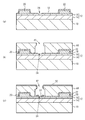
図3は、実施例1に係る半導体装置の断面図の例である。図3のように、ゲート電極50は、開口24に埋め込まれるように第1絶縁膜18上に設けられたNi層52からなる金属パターンと、Ni層52の上面と側面とを覆うPd層54からなるバリア層と、Pd層54上に設けられたAu層56からなる導電層と、を有する。Ni層52は、窒化物半導体層12に対してショットキ接合を構成する。Pd層54のゲート長方向の長さとAu層56のゲート長方向の長さとは同じである。つまり、ゲート電極50の断面は、上部に向かっても幅は一定となっている。Ni層52の厚さは、例えば30nmである。Pd層54の厚さは、例えば60nmである。Au層56の厚さは、例えば500nmである。また、後述の実施例1に係る半導体装置の製造方法で詳しく説明するが、Ni層52は真空蒸着法によって形成され、Pd層54とAu層56とは無電解めっき法によって形成される。その他の構成は比較例1の図1と同じであるため、説明を省略する。
FIG. 3 is an example of a cross-sectional view of the semiconductor device according to the first embodiment. As shown in FIG. 3, the
次に、実施例1に係る半導体装置の製造方法について説明する。図4(a)から図5(c)は、実施例1に係る半導体装置の製造方法を示す断面図である。図4(a)のように、SiC基板である基板10上に、窒化物半導体層12として、GaN層であるチャネル層14とAlGaN層である電子供給層16とをこの順に成長させる。チャネル層14及び電子供給層16の成長は、MOCVD法(有機金属気相成長法)を用いることができる。窒化物半導体層12上に、真空蒸着法及びリフトオフ法を用いて、窒化物半導体層12側からTi層とAl層とがこの順に積層された金属層を形成する。その後、例えば500℃から800℃の温度で金属層に対してアニール処理を行い、窒化物半導体層12にオーミック接合するオーミック電極であるソース電極20及びドレイン電極22を形成する。ソース電極20とドレイン電極22とを覆うように、窒化物半導体層12上に、プラズマCVD法(プラズマ化学気相成長法)を用いて、窒化シリコン膜である第1絶縁膜18を形成する。ソース電極20とドレイン電極22との間であって、ゲート電極を形成すべき領域の第1絶縁膜18を除去して開口24を形成する。開口24の底面は、窒化物半導体層12が露出している。これにより、窒化物半導体層12上に、開口24を有する第1絶縁膜18が形成される。
Next, a method for manufacturing the semiconductor device according to the first embodiment will be described. 4A to 5C are cross-sectional views illustrating the method for manufacturing the semiconductor device according to the first embodiment. As shown in FIG. 4A, a
図4(b)のように、第1絶縁膜18上に、開口24に対応する位置に開口24よりも大きな第1開口42を有するマスク層である第1レジスト層44を形成する。第1レジスト層44は、第1開口42において上側部分が下側部分よりも突き出た形状をしている。このような形状の第1レジスト層44は、フォトプロセスを2回繰り返すことによって形成できる。なお、第1レジスト層44は、第1開口42において逆テーパ形状をしている場合でもよい。
As shown in FIG. 4B, a first resist
図4(c)のように、第1レジスト層44をマスクとして、真空蒸着法を用いてNiからなる金属パターンを堆積する。これにより、窒化物半導体層12上に、上面および側面を有し、Niを含有する金属パターンが形成される。つまり、開口24内の窒化物半導体層12上及び第1絶縁膜18上に、Ni層52が形成される。典型的にNi層52は、真空蒸着法で形成されるため、上部に向かうほど幅が狭まる断面形状となる。
As shown in FIG. 4C, a metal pattern made of Ni is deposited by vacuum evaporation using the first resist
図5(a)のように、第1レジスト層44を除去した後、第1絶縁膜18上に、Ni層52のゲート長方向の幅よりも大きい幅を有する第2開口46がNi層52に対応して形成されたマスク層である第2レジスト層48を形成する。次に、第2レジスト層48をマスクとして、無電解めっき法により、第2開口46内にPdを充填して成長させる。このPdは、Niの拡散に対するバリア層である。無電解めっき法では、Pdは下地活性層となるNi層52に対して等方的に成長する。このため、Pd層54が、Ni層52の露出面、即ち、Ni層52(金属パターン)の上面および側面を被覆するように形成される。これにより、Ni層52(金属パターン)の表面がバリア層であるPd層54で被覆される。なお、窒化物半導体層12上に第1絶縁膜18が形成されているため、Pd層54と窒化物半導体層12との間は第1絶縁膜18によって隔離されて、Pd層54は窒化物半導体層12に接することなく形成される。続いて、無電解めっき法により、第2開口46内をAuで充填して、導電層としてAuを成長させる。これにより、Pd層54上にAu層56が形成される。これらによって、Ni層52、Pd層54、及びAu層56を有するゲート電極50が形成される。Pd層54及びAu層56の幅W1は、第2レジスト層48の第2開口46の幅で規定され、例えば1.0μmである。第1絶縁膜18の上面に接する部分におけるNi層52の幅W2は、例えば0.8μmである。Ni層52の上部の幅W3は、例えば0.6μmである。
As shown in FIG. 5A, after the first resist
図5(b)のように、第2レジスト層48を除去した後、ゲート電極50を覆うように、プラズマCVD法を用いて、窒化シリコン膜である第2絶縁膜34を形成する。第2絶縁膜34には、ゲート電極50の段差の形状を反映した段差が形成される。
As shown in FIG. 5B, after the second resist layer 48 is removed, a second insulating
図5(c)のように、ソース電極20上及びドレイン電極22上の第2絶縁膜34と第1絶縁膜18とを除去して開口を形成する。この開口内及び第2絶縁膜34上に、めっき法を用いて、金属層を形成する。金属層は、ソース電極20の上面に接するソース配線36、ドレイン電極22の上面に接するドレイン配線38、及び第2絶縁膜34の段差を覆う位置に設けられたフィールドプレート40を含む。これにより、実施例1に係る半導体装置が完成する。
As shown in FIG. 5C, the second insulating
実施例1によれば、図3のように、ゲート電極50は、開口24に埋め込まれるように第1絶縁膜18上に設けられ、上面および側面を有するNi層52と、Ni層52の上面及び側面を覆うPd層54と、Pd層54上に設けられたAu層56と、を有する。Pd層54によって、Ni層52は、第2絶縁膜34及びAu層56に接することなく設けられている。これにより、Pd層54が、Ni層52に含まれるNiの拡散を抑制するバリア層として機能し、Ni層52のNiが第2絶縁膜34に拡散することを抑制できる。よって、半導体装置の故障を抑制できる。
According to the first embodiment, as shown in FIG. 3, the
Ni層52の上面及び側面を被覆するPd層54は、図5(a)で説明したように、無電解めっき法により形成される。無電解めっき法は、上述したように、めっき層が下地活性層に対して等方的に成長するため、Pd層54は、Ni層52の上面及び側面を含む露出面を被覆し、Ni層52の表面を覆って形成される。また、Pd層54が等方的に成長することから、Ni層52の上面に形成された、開口24の段差に起因した段差部分も十分な厚さで被覆することができる。例えば、図2のように、Pd層30を真空蒸着法で形成した場合、蒸着源から基板10に対して垂直に蒸着粒子が入射するよう、蒸着源と基板10との位置関係が設定されるため、Ni層28の上面の段差部分を十分な厚さのPd層30で被覆することが難しい。このため、Ni層28のNiがAu層32に拡散し、その結果、Niが第2絶縁膜34に拡散してしまう。しかしながら、実施例1では、Pd層54を無電解めっき法で形成することで、Ni層52の上面の段差部分を十分な厚さのPd層54で被覆することができるため、Ni層52のNiがAu層56を経由して第2絶縁膜34に拡散することを抑制できる。
As described with reference to FIG. 5A, the
ここで、Pd層及びAu層を無電解めっき法ではなく、電解めっき法で形成した場合の問題点について説明する。図6(a)及び図6(b)は、Pd層及びAu層を電解めっき法で形成する工程を示す断面図である。図6(a)のように、窒化物半導体層12上に形成された第1絶縁膜18の開口24に埋め込まれるように、真空蒸着法又はスパッタ法を用いて、第1絶縁膜18上にNi層72を形成する。ここで、Ni層72をPd層及びAu層を電解めっき法で形成する際のシード層として用いるために、基板10上全面にNi層72を残存させておく。
Here, a problem when the Pd layer and the Au layer are formed not by electroless plating but by electrolytic plating will be described. FIGS. 6A and 6B are cross-sectional views showing a process of forming a Pd layer and an Au layer by an electrolytic plating method. As shown in FIG. 6A, the first insulating
Ni層72上に、開口24よりも大きな開口を有するレジスト層78を形成する。レジスト層78をマスクとして、電解めっき法を用いて、Ni層72上に、Pd層74とAu層76とを順に成長させる。
A resist
図6(b)のように、レジスト層78を除去した後、Au層76とPd層74とをマスクとして、Ni層72をエッチングする。これにより、Ni層72、Pd層74、及びAu層76を有するゲート電極70が形成される。
As shown in FIG. 6B, after removing the resist
このように、Pd層74とAu層76とを電解めっき法で形成する場合、Ni層72をシード層として用いるため、図6(b)のように、Pd層74とAu層76とを形成した後、Ni層72をエッチングして除去することがなされる。このため、Ni層72の側面をPd層74で覆うことができず、Ni層72のNiが第2絶縁膜34に拡散することが生じてしまう。このように、Pd層74及びAu層76を電解めっき法を用いて形成する場合では、Ni層72のNiが拡散してしまうことを抑制できない。したがって、実施例1では、Pd層54とAu層56とを無電解めっき法を用いて形成している。
In this way, when the
また、ゲート電極の抵抗を低減させるためにAu層を設けているが、図2のように、ゲート電極26を真空蒸着法で形成する場合、ゲート電極26の上側ほど幅が狭い断面形状となる。このため、Au層32を厚くしても、ゲート電極26の抵抗を低減させる効果が小さい。一方、実施例1では、Pd層54とAu層56とを無電解めっき法で形成しているため、矩形形状をしたゲート電極50が得られる。このため、Au層56を厚くすることで、ゲート電極50の抵抗を効果的に低減させることができる。
In addition, although an Au layer is provided to reduce the resistance of the gate electrode, as shown in FIG. 2, when the
さらに、図2のように、Pd層30とAu層32とを真空蒸着法で形成する場合は、ウエハである基板10の外周部でパターンの位置ずれが生じる場合がある。これは、蒸着源に比べて、ウエハが遥かに大きいためである。一方、実施例1では、Pd層54とAu層56とは無電解めっき法で形成しているため、Ni層52に対してPd層54とAu層56とのパターンの位置がずれることを抑制できる。
Furthermore, as shown in FIG. 2, when the
Ni層52の厚さは、30nmの場合に限られず、10nm以上且つ100nm以下の場合でもよい。Pd層54の厚さは、60nmの場合に限られず、10nm以上且つ80nm以下の場合でよい。Au層56の厚さは、500nmの場合に限られず、200nm以上且つ1000nm以下の場合でもよい。また、第1絶縁膜18の厚さは、30nmの場合に限られず、10nm以上且つ100nm以下の場合でもよい。ただし、Ni層52の厚さに対する第1絶縁膜18の厚さの比(即ち、第1絶縁膜18の厚さ/Ni層52の厚さ)は、0.5以上且つ1.5以下である場合が好ましい。この第1絶縁膜18の厚さ/Ni層52の厚さの比が1.5より大きい場合、開口24において、第1絶縁膜18上に堆積したNi層52と、開口24に埋め込まれたNi層52とが、物理的に乖離した段切れ状態となるため、1.5以下の場合が好ましい。また、第1絶縁膜18の厚さ/Ni層52の厚さの比が0.5以上のとき、真空蒸着法において、Ni層52の上面に形成される、開口24の段差に起因した段差部分が問題となるが、実施例1ではPd層54を無電解めっき法で形成することで、Ni層52の上面の段差部分を十分な厚さのPd層54で被覆することができ、Ni層52のNiがAu層56を経由して第2絶縁膜34に拡散することを抑制できるため、0.5以上の場合にも問題がない。
The thickness of the
また、Ni層52の側面におけるPd層54の厚さ(図5(a)におけるW1−W2)は、Niの拡散を抑制するために、0.2μm以上の場合が好ましく、0.3μm以上の場合がより好ましく、0.4μm以上の場合がさらに好ましい。
Further, the thickness of the
図3のように、フィールドプレート40は、ゲート電極50の段差の形状を反映して形成された第2絶縁膜34の段差を覆う位置に設けられ、ゲート電極50に沿ってゲート電極50上まで延在している場合を例に示した。しかしながら、図7(a)の実施例1の変形例1に係るFETのように、フィールドプレート80が、ゲート電極50とドレイン電極22との間に位置し、ゲート電極50上まで延在していない場合でもよい。なお、フィールドプレート80も、フィールドプレート40と同様に、Auめっき層等の金属層からなり、FETの活性領域外でソース配線36に接続されている。
As shown in FIG. 3, the
第2絶縁膜34上に形成されるフィールドプレート40、80は、ソース電極20に電気的に接続されている場合に限られず、ソース電極20に電気的に接続されていない場合でもよい。フィールドプレート40、80は、浮き導体の場合でもよい。この場合でも、ゲート電極50のNi層52に含まれるNiがフィールドプレート40、80に向かって第2絶縁膜34を拡散し易いため、Ni層52の上面と側面とを覆ってPd層54を設けることが有効である。しかしながら、フィールドプレート40、80がソース電極20に電気的に接続されている場合は、ゲート電極50のNi層52に含まれるNiがフィールドプレート40、80に向かって第2絶縁膜34をより拡散し易い。したがって、フィールドプレート40、80がソース電極20に電気的に接続されている場合に、Ni層52の上面と側面とを覆ってPd層54を設けることがより有効である。
The
また、フィールドプレート40の代わりに、図7(b)の実施例1の変形例2に係るFETのように、ソースウォール82が設けられている場合でもよい。ソースウォール82は、Auめっき層等の金属層からなり、ソース配線36に接続され、第2絶縁膜34上でゲート電極50を覆うように、ソース配線36から第2絶縁膜34の段差を覆う位置に延在して設けられている。ソースウォール82は、ソース電極20に電気的に接続されているため、ゲート電極50のNi層52に含まれるNiがソースウォール82に向かって第2絶縁膜34を拡散し易い。したがって、ソースウォール82が設けられている場合に、Ni層52の上面と側面とを覆ってPd層54を設けることがより有効である。
Further, instead of the
図5(a)のように、Ni層52に対してソース電極20側及びドレイン電極22側に対称な形状の第2開口46を有する第2レジスト層48をマスクとして、無電解めっき法にてPd層54及びAu層56を形成しているが、これに限られない。図8は、ゲート電極50を形成する工程の第1の変形例を示す断面図である。図8のように、Ni層52に対してソース電極20側及びドレイン電極22側に非対称な形状の第2開口90を有する第2レジスト層92をマスクとして、無電解めっき法にてPd層54とAu層56とを形成してもよい。この場合、ドレイン側に延びたゲート電極により、ショットキ接合近傍へのキャリアトラップを低減することができ、ドレイン電流のコラプス現象を低減することが可能となる。
As shown in FIG. 5A, the second resist layer 48 having the
また、図5(a)のように、第1レジスト層44を除去した後、Ni層52の幅よりも大きい第2開口46を有する第2レジスト層48を形成し、これをマスクとして、無電解めっき法にてPd層54とAu層56とを形成しているが、これに限られない。図9は、ゲート電極50を形成する工程の第2の変形例を示す断面図である。図9のように、Pd層54とAu層56とのパターンの大きさに制約がなく、余裕がある場合には、第2レジスト層48を形成することなく、無電解めっき法にてPd層54とAu層56とを形成してもよい。これにより、第2レジスト層48を形成する工程を省くことができるため、製造工程を短縮できる。
Further, as shown in FIG. 5A, after the first resist
Ni層52は、真空蒸着法を用いて形成する場合に限られず、スパッタ法を用いて形成してもよい。また、真空蒸着法又はスパッタ法にてNiを数nm堆積した後、無電解めっき法にてNi、Pd、Auを連続して成長させて、Ni層52、Pd層54、及びAu層56を有するゲート電極50を形成してもよい。
The
窒化物半導体層12上に、開口24を有する第1絶縁膜18が設けられている場合に、FETの活性化処理を適切に実施すれば、開口24の窒化物半導体層12上からのみ無電解めっき金属を成長させることができる。したがって、活性化処理を適切に行い、Ni層52、Pd層54、及びAu層56の全てを無電解めっき法にて形成する場合でもよい。
In the case where the first insulating
図3のように、開口24に埋め込まれるように第1絶縁膜18上にNi層52が設けられているが、Ni層52の場合に限られず、Niを含有する金属パターンであればよい。Niを含有する金属パターンの例として、Ni層の他に、Niと他の金属とを含む層の場合や、Ni層と他の金属層との積層の場合が挙げられる。
As shown in FIG. 3, the
Ni層52の上面及び側面を覆う金属層が、Ni層52の上面及び側面を覆うPd層54と、Pd層54上に設けられたAu層56と、を含む場合を例に示したが、これに限られる訳ではない。Ni層52に含まれるNiが拡散することを抑制するバリア層として機能すれば、Ni層52の上面及び側面をPd層54以外のバリア層、例えばPt(白金)層で覆っている場合でもよい。また、ゲート電極50の抵抗が低減すれば、Pd層54上にAu層56以外の低抵抗の導電層、例えばCu(銅)が設けられている場合でもよい。
The case where the metal layer covering the upper surface and the side surface of the
基板10は、SiC基板の他にも、例えばSi基板、サファイア基板、又はGaN基板等、その他の基板を用いることができる。基板10上に形成される窒化物半導体層としては、GaN層、InN層、AlN層、InGaN層、AlGaN層、InAlN層、及びInAlGaN層のうちの少なくとも1つを含む単層又は積層を用いることができる。第1絶縁膜18及び第2絶縁膜34は、窒化シリコン膜以外の絶縁膜、例えば酸化シリコン膜を用いてもよい。
In addition to the SiC substrate, the
実施例1では、HEMTの場合を例に示したが、MESFET(Metal Semiconductor Field Effect Transistor)等、その他のFETの場合でもよいし、FET以外の半導体装置の場合でもよい。また、第2絶縁膜34上にフィールドプレート又はソースウォールを構成する金属層が設けられている場合を例に示したが、金属層が設けられていない場合でもよい。この場合でも、Ni層52のNiが第2絶縁膜34に拡散することがあるため、Ni層52の上面及び側面をPd層54で覆うことが望ましい。
In the first embodiment, the case of HEMT has been described as an example, but other FETs such as a MESFET (Metal Semiconductor Field Effect Transistor) may be used, or a semiconductor device other than the FET may be used. Moreover, although the case where the metal layer which comprises a field plate or a source wall is provided on the 2nd insulating
以上、本発明の実施例について詳述したが、本発明はかかる特定の実施例に限定されるものではなく、特許請求の範囲に記載された本発明の要旨の範囲内において、種々の変形・変更が可能である。 Although the embodiments of the present invention have been described in detail above, the present invention is not limited to such specific embodiments, and various modifications and changes can be made within the scope of the gist of the present invention described in the claims. It can be changed.
10 基板
12 窒化物半導体層
14 チャネル層
16 電子供給層
18 第1絶縁膜
20 ソース電極
22 ドレイン電極
24 開口
26、50 ゲート電極
28、52 Ni層
30、54 Pd層
32、56 Au層
34 第2絶縁膜
36 ソース配線
38 ドレイン配線
40、80 フィールドプレート
42 第1開口
44 第1レジスト層
46 第2開口
48 第2レジスト層
82 ソースウォール
10
Claims (7)
前記金属パターンの前記上面および前記外側面を含む露出面に対して無電解めっきによってバリア層を形成し、前記金属パターンの前記上面および前記外側面を前記バリア層で被覆する工程と、
前記バリア層上に、無電解めっきによって導電層を形成する工程と、
前記窒化物半導体層上に、前記導電層を覆う絶縁膜を形成する工程と、を有することを特徴とする半導体装置の製造方法。 A nitride semiconductor layer having a top surface and outer side surface, forming a metal pattern containing nickel,
A step of forming a barrier layer, covering the upper surface and the outer surface of the metal pattern in the barrier layer by electroless plating to the exposed surface including said top surface and said outer surface of said metal pattern,
Forming a conductive layer on the barrier layer by electroless plating;
And a step of forming an insulating film covering the conductive layer on the nitride semiconductor layer .
前記金属パターンは、前記他の絶縁膜および前記開口に接して形成され、
前記金属パターンの前記外側面に形成された前記バリア層と前記窒化物半導体層との間は、前記他の絶縁膜によって隔離されてなることを特徴とする請求項1記載の半導体装置の製造方法。 Forming another insulating film having an opening on the nitride semiconductor layer;
The metal pattern is formed in contact with the other insulating film and the opening,
The method for manufacturing a semiconductor device according to claim 1 , wherein the barrier layer formed on the outer surface of the metal pattern and the nitride semiconductor layer are separated by the other insulating film. .
前記絶縁膜の前記段差の位置に金属層を形成する工程を有することを特徴とする請求項1から4のいずれか一項記載の半導体装置の製造方法。 The insulating film has a step reflecting the shape of the step of the barrier layer and the conductive layer,
5. The method of manufacturing a semiconductor device according to claim 1 , further comprising a step of forming a metal layer at the level difference of the insulating film .
Priority Applications (3)
| Application Number | Priority Date | Filing Date | Title |
|---|---|---|---|
| JP2012147538A JP5983999B2 (en) | 2012-06-29 | 2012-06-29 | Manufacturing method of semiconductor device |
| US13/930,904 US9412829B2 (en) | 2012-06-29 | 2013-06-28 | Method for fabricating semiconductor device and semiconductor device |
| US15/204,199 US9653592B2 (en) | 2012-06-29 | 2016-07-07 | Method for fabricating semiconductor device and semiconductor device |
Applications Claiming Priority (1)
| Application Number | Priority Date | Filing Date | Title |
|---|---|---|---|
| JP2012147538A JP5983999B2 (en) | 2012-06-29 | 2012-06-29 | Manufacturing method of semiconductor device |
Publications (3)
| Publication Number | Publication Date |
|---|---|
| JP2014011350A JP2014011350A (en) | 2014-01-20 |
| JP2014011350A5 JP2014011350A5 (en) | 2015-05-21 |
| JP5983999B2 true JP5983999B2 (en) | 2016-09-06 |
Family
ID=49777263
Family Applications (1)
| Application Number | Title | Priority Date | Filing Date |
|---|---|---|---|
| JP2012147538A Active JP5983999B2 (en) | 2012-06-29 | 2012-06-29 | Manufacturing method of semiconductor device |
Country Status (2)
| Country | Link |
|---|---|
| US (2) | US9412829B2 (en) |
| JP (1) | JP5983999B2 (en) |
Families Citing this family (17)
| Publication number | Priority date | Publication date | Assignee | Title |
|---|---|---|---|---|
| US9178016B2 (en) * | 2013-03-01 | 2015-11-03 | Infineon Technologies Austria Ag | Charge protection for III-nitride devices |
| JP6179445B2 (en) * | 2014-04-11 | 2017-08-16 | 豊田合成株式会社 | Vertical Schottky Barrier Diode, Manufacturing Method for Vertical Schottky Barrier Diode |
| JP2015204335A (en) * | 2014-04-11 | 2015-11-16 | 豊田合成株式会社 | Semiconductor device and method for manufacturing semiconductor device |
| EP2942815B1 (en) * | 2014-05-08 | 2020-11-18 | Nexperia B.V. | Semiconductor device and manufacturing method |
| CN104332498B (en) * | 2014-09-01 | 2018-01-05 | 苏州捷芯威半导体有限公司 | A kind of tiltedly preparation method of field plate power device and oblique field plate power device |
| JP6292104B2 (en) * | 2014-11-17 | 2018-03-14 | 三菱電機株式会社 | Manufacturing method of nitride semiconductor device |
| JP2017107942A (en) * | 2015-12-08 | 2017-06-15 | 株式会社東芝 | Semiconductor device |
| WO2018188649A1 (en) * | 2017-04-14 | 2018-10-18 | 苏州能讯高能半导体有限公司 | Semiconductor device and manufacturing method therefor |
| WO2018225195A1 (en) * | 2017-06-07 | 2018-12-13 | 三菱電機株式会社 | Semiconductor device production method |
| JP6997002B2 (en) * | 2018-02-19 | 2022-01-17 | 住友電気工業株式会社 | Semiconductor devices and their manufacturing methods |
| JP7047615B2 (en) * | 2018-06-13 | 2022-04-05 | 住友電工デバイス・イノベーション株式会社 | Manufacturing method of semiconductor device |
| CN109449211B (en) * | 2018-11-01 | 2022-06-07 | 合肥鑫晟光电科技有限公司 | Thin film transistor and manufacturing method thereof, array substrate and manufacturing method thereof |
| US11955522B2 (en) * | 2020-02-13 | 2024-04-09 | Vanguard International Semiconductor Corporation | Semiconductor structure and method of forming the same |
| DE112021006913T5 (en) * | 2021-01-27 | 2023-11-16 | Mitsubishi Electric Corporation | Semiconductor device and method for producing same |
| JP2022145319A (en) * | 2021-03-19 | 2022-10-04 | 株式会社東芝 | Semiconductor device |
| CN113725283A (en) * | 2021-11-04 | 2021-11-30 | 深圳市时代速信科技有限公司 | Semiconductor device and method for manufacturing the same |
| CN113793867B (en) * | 2021-11-16 | 2022-03-01 | 深圳市时代速信科技有限公司 | Electrode structure and manufacturing method thereof |
Family Cites Families (11)
| Publication number | Priority date | Publication date | Assignee | Title |
|---|---|---|---|---|
| US5014018A (en) * | 1987-10-06 | 1991-05-07 | Stanford University | Nonlinear transmission line for generation of picosecond electrical transients |
| JP2643812B2 (en) * | 1993-12-24 | 1997-08-20 | 日本電気株式会社 | Method for forming gate electrode of field effect transistor |
| JPH0897234A (en) * | 1994-09-22 | 1996-04-12 | Mitsubishi Electric Corp | Electrode of semiconductor device and its manufacture |
| JPH11121471A (en) * | 1997-10-21 | 1999-04-30 | Nec Corp | Semiconductor apparatus and manufacture thereof |
| JP2003179057A (en) * | 2001-12-12 | 2003-06-27 | Sony Corp | Semiconductor device and method of manufacturing the same |
| JP2003273129A (en) * | 2002-03-14 | 2003-09-26 | Fujitsu Quantum Devices Ltd | Semiconductor device and manufacturing method thereof |
| JP2006261252A (en) | 2005-03-15 | 2006-09-28 | Eudyna Devices Inc | Semiconductor device and manufacturing method thereof |
| US8212290B2 (en) * | 2007-03-23 | 2012-07-03 | Cree, Inc. | High temperature performance capable gallium nitride transistor |
| US7935620B2 (en) * | 2007-12-05 | 2011-05-03 | Freescale Semiconductor, Inc. | Method for forming semiconductor devices with low leakage Schottky contacts |
| JP2011238805A (en) * | 2010-05-11 | 2011-11-24 | Nec Corp | Field effect transistor, method of manufacturing field effect transistor and electronic device |
| US20120156843A1 (en) * | 2010-12-17 | 2012-06-21 | Green Bruce M | Dielectric layer for gallium nitride transistor |
-
2012
- 2012-06-29 JP JP2012147538A patent/JP5983999B2/en active Active
-
2013
- 2013-06-28 US US13/930,904 patent/US9412829B2/en active Active
-
2016
- 2016-07-07 US US15/204,199 patent/US9653592B2/en active Active
Also Published As
| Publication number | Publication date |
|---|---|
| US20160315181A1 (en) | 2016-10-27 |
| US20140001640A1 (en) | 2014-01-02 |
| JP2014011350A (en) | 2014-01-20 |
| US9412829B2 (en) | 2016-08-09 |
| US9653592B2 (en) | 2017-05-16 |
Similar Documents
| Publication | Publication Date | Title |
|---|---|---|
| JP5983999B2 (en) | Manufacturing method of semiconductor device | |
| JP6335444B2 (en) | III-nitride transistor using regrowth structure | |
| US11222969B2 (en) | Normally-off transistor with reduced on-state resistance and manufacturing method | |
| TWI431770B (en) | Semiconductor device and method for manufacturing the same | |
| TWI512993B (en) | Transistor and method of forming the same and semiconductor device | |
| US11316038B2 (en) | HEMT transistor with adjusted gate-source distance, and manufacturing method thereof | |
| JP2012231109A (en) | Nitride semiconductor element and manufacturing method for the same | |
| JP2011155221A (en) | Semiconductor device and method of manufacturing the same | |
| US11335797B2 (en) | Semiconductor devices and methods for fabricating the same | |
| US9564503B2 (en) | Semiconductor device and method of manufacturing semiconductor device | |
| JP2012069978A (en) | Compound semiconductor device | |
| TW201933490A (en) | Semiconductor devices and methods for fabricating the same | |
| JP5504660B2 (en) | Compound semiconductor device and manufacturing method thereof | |
| JP6166508B2 (en) | Semiconductor device and manufacturing method of semiconductor device | |
| JP2019047055A (en) | Transistor | |
| KR20150030283A (en) | Power semiconductor device | |
| US10903350B2 (en) | Semiconductor devices and methods for forming the same | |
| US20100117186A1 (en) | Semiconductor device and method of producing the same | |
| US20240047554A1 (en) | Semiconductor device and manufacturing method thereof | |
| WO2023141749A1 (en) | GaN-BASED SEMICONDUCTOR DEVICE WITH REDUCED LEAKAGE CURRENT AND METHOD FOR MANUFACTURING THE SAME | |
| US20230015042A1 (en) | Semiconductor device and manufacturing method thereof | |
| JP2013211484A (en) | Semiconductor device manufacturing method |
Legal Events
| Date | Code | Title | Description |
|---|---|---|---|
| A521 | Request for written amendment filed |
Free format text: JAPANESE INTERMEDIATE CODE: A523 Effective date: 20150330 |
|
| A621 | Written request for application examination |
Free format text: JAPANESE INTERMEDIATE CODE: A621 Effective date: 20150330 |
|
| A977 | Report on retrieval |
Free format text: JAPANESE INTERMEDIATE CODE: A971007 Effective date: 20160114 |
|
| A131 | Notification of reasons for refusal |
Free format text: JAPANESE INTERMEDIATE CODE: A131 Effective date: 20160126 |
|
| A521 | Request for written amendment filed |
Free format text: JAPANESE INTERMEDIATE CODE: A523 Effective date: 20160315 |
|
| TRDD | Decision of grant or rejection written | ||
| A01 | Written decision to grant a patent or to grant a registration (utility model) |
Free format text: JAPANESE INTERMEDIATE CODE: A01 Effective date: 20160705 |
|
| A61 | First payment of annual fees (during grant procedure) |
Free format text: JAPANESE INTERMEDIATE CODE: A61 Effective date: 20160720 |
|
| R150 | Certificate of patent or registration of utility model |
Ref document number: 5983999 Country of ref document: JP Free format text: JAPANESE INTERMEDIATE CODE: R150 |
|
| R250 | Receipt of annual fees |
Free format text: JAPANESE INTERMEDIATE CODE: R250 |
|
| R250 | Receipt of annual fees |
Free format text: JAPANESE INTERMEDIATE CODE: R250 |
|
| R250 | Receipt of annual fees |
Free format text: JAPANESE INTERMEDIATE CODE: R250 |
|
| R250 | Receipt of annual fees |
Free format text: JAPANESE INTERMEDIATE CODE: R250 |
|
| R250 | Receipt of annual fees |
Free format text: JAPANESE INTERMEDIATE CODE: R250 |