JP5912808B2 - 半導体装置 - Google Patents
半導体装置 Download PDFInfo
- Publication number
- JP5912808B2 JP5912808B2 JP2012099687A JP2012099687A JP5912808B2 JP 5912808 B2 JP5912808 B2 JP 5912808B2 JP 2012099687 A JP2012099687 A JP 2012099687A JP 2012099687 A JP2012099687 A JP 2012099687A JP 5912808 B2 JP5912808 B2 JP 5912808B2
- Authority
- JP
- Japan
- Prior art keywords
- inductor
- semiconductor device
- current path
- current
- horseshoe
- Prior art date
- Legal status (The legal status is an assumption and is not a legal conclusion. Google has not performed a legal analysis and makes no representation as to the accuracy of the status listed.)
- Active
Links
- 239000004065 semiconductor Substances 0.000 title claims description 39
- 230000005540 biological transmission Effects 0.000 claims description 20
- 239000002184 metal Substances 0.000 description 21
- 238000010586 diagram Methods 0.000 description 17
- 238000004891 communication Methods 0.000 description 16
- 239000004020 conductor Substances 0.000 description 10
- 239000003990 capacitor Substances 0.000 description 9
- 238000000034 method Methods 0.000 description 9
- 238000004804 winding Methods 0.000 description 8
- 230000002441 reversible effect Effects 0.000 description 4
- 230000008878 coupling Effects 0.000 description 3
- 238000010168 coupling process Methods 0.000 description 3
- 238000005859 coupling reaction Methods 0.000 description 3
- 230000004907 flux Effects 0.000 description 3
- 230000000149 penetrating effect Effects 0.000 description 3
- 239000000758 substrate Substances 0.000 description 3
- 230000001413 cellular effect Effects 0.000 description 2
- 239000012535 impurity Substances 0.000 description 2
- 239000012212 insulator Substances 0.000 description 2
- 230000007774 longterm Effects 0.000 description 2
- 238000010295 mobile communication Methods 0.000 description 2
- 238000012986 modification Methods 0.000 description 2
- 230000004048 modification Effects 0.000 description 2
- 230000010363 phase shift Effects 0.000 description 2
- 230000004044 response Effects 0.000 description 2
- 238000010897 surface acoustic wave method Methods 0.000 description 2
- 230000002238 attenuated effect Effects 0.000 description 1
- 230000003247 decreasing effect Effects 0.000 description 1
- 230000006866 deterioration Effects 0.000 description 1
- 239000004973 liquid crystal related substance Substances 0.000 description 1
- 238000004519 manufacturing process Methods 0.000 description 1
- 230000010355 oscillation Effects 0.000 description 1
- 230000003071 parasitic effect Effects 0.000 description 1
- 230000035945 sensitivity Effects 0.000 description 1
Images


Classifications
-
- H—ELECTRICITY
- H04—ELECTRIC COMMUNICATION TECHNIQUE
- H04B—TRANSMISSION
- H04B1/00—Details of transmission systems, not covered by a single one of groups H04B3/00 - H04B13/00; Details of transmission systems not characterised by the medium used for transmission
- H04B1/38—Transceivers, i.e. devices in which transmitter and receiver form a structural unit and in which at least one part is used for functions of transmitting and receiving
- H04B1/40—Circuits
-
- H—ELECTRICITY
- H01—ELECTRIC ELEMENTS
- H01F—MAGNETS; INDUCTANCES; TRANSFORMERS; SELECTION OF MATERIALS FOR THEIR MAGNETIC PROPERTIES
- H01F17/00—Fixed inductances of the signal type
- H01F17/0006—Printed inductances
-
- H—ELECTRICITY
- H01—ELECTRIC ELEMENTS
- H01F—MAGNETS; INDUCTANCES; TRANSFORMERS; SELECTION OF MATERIALS FOR THEIR MAGNETIC PROPERTIES
- H01F17/00—Fixed inductances of the signal type
- H01F17/0006—Printed inductances
- H01F17/0013—Printed inductances with stacked layers
-
- H—ELECTRICITY
- H01—ELECTRIC ELEMENTS
- H01F—MAGNETS; INDUCTANCES; TRANSFORMERS; SELECTION OF MATERIALS FOR THEIR MAGNETIC PROPERTIES
- H01F38/00—Adaptations of transformers or inductances for specific applications or functions
- H01F38/14—Inductive couplings
-
- H—ELECTRICITY
- H01—ELECTRIC ELEMENTS
- H01L—SEMICONDUCTOR DEVICES NOT COVERED BY CLASS H10
- H01L23/00—Details of semiconductor or other solid state devices
- H01L23/52—Arrangements for conducting electric current within the device in operation from one component to another, i.e. interconnections, e.g. wires, lead frames
- H01L23/522—Arrangements for conducting electric current within the device in operation from one component to another, i.e. interconnections, e.g. wires, lead frames including external interconnections consisting of a multilayer structure of conductive and insulating layers inseparably formed on the semiconductor body
- H01L23/5227—Inductive arrangements or effects of, or between, wiring layers
-
- H—ELECTRICITY
- H01—ELECTRIC ELEMENTS
- H01L—SEMICONDUCTOR DEVICES NOT COVERED BY CLASS H10
- H01L28/00—Passive two-terminal components without a potential-jump or surface barrier for integrated circuits; Details thereof; Multistep manufacturing processes therefor
- H01L28/10—Inductors
-
- H—ELECTRICITY
- H04—ELECTRIC COMMUNICATION TECHNIQUE
- H04L—TRANSMISSION OF DIGITAL INFORMATION, e.g. TELEGRAPHIC COMMUNICATION
- H04L25/00—Baseband systems
- H04L25/02—Details ; arrangements for supplying electrical power along data transmission lines
- H04L25/03—Shaping networks in transmitter or receiver, e.g. adaptive shaping networks
- H04L25/03006—Arrangements for removing intersymbol interference
- H04L25/03343—Arrangements at the transmitter end
-
- H—ELECTRICITY
- H04—ELECTRIC COMMUNICATION TECHNIQUE
- H04L—TRANSMISSION OF DIGITAL INFORMATION, e.g. TELEGRAPHIC COMMUNICATION
- H04L27/00—Modulated-carrier systems
- H04L27/32—Carrier systems characterised by combinations of two or more of the types covered by groups H04L27/02, H04L27/10, H04L27/18 or H04L27/26
- H04L27/34—Amplitude- and phase-modulated carrier systems, e.g. quadrature-amplitude modulated carrier systems
- H04L27/36—Modulator circuits; Transmitter circuits
- H04L27/366—Arrangements for compensating undesirable properties of the transmission path between the modulator and the demodulator
-
- H—ELECTRICITY
- H01—ELECTRIC ELEMENTS
- H01F—MAGNETS; INDUCTANCES; TRANSFORMERS; SELECTION OF MATERIALS FOR THEIR MAGNETIC PROPERTIES
- H01F17/00—Fixed inductances of the signal type
- H01F17/0006—Printed inductances
- H01F2017/0073—Printed inductances with a special conductive pattern, e.g. flat spiral
-
- H—ELECTRICITY
- H01—ELECTRIC ELEMENTS
- H01F—MAGNETS; INDUCTANCES; TRANSFORMERS; SELECTION OF MATERIALS FOR THEIR MAGNETIC PROPERTIES
- H01F17/00—Fixed inductances of the signal type
- H01F17/0006—Printed inductances
- H01F2017/0086—Printed inductances on semiconductor substrate
-
- H—ELECTRICITY
- H01—ELECTRIC ELEMENTS
- H01F—MAGNETS; INDUCTANCES; TRANSFORMERS; SELECTION OF MATERIALS FOR THEIR MAGNETIC PROPERTIES
- H01F38/00—Adaptations of transformers or inductances for specific applications or functions
- H01F38/14—Inductive couplings
- H01F2038/143—Inductive couplings for signals
-
- H—ELECTRICITY
- H01—ELECTRIC ELEMENTS
- H01L—SEMICONDUCTOR DEVICES NOT COVERED BY CLASS H10
- H01L2924/00—Indexing scheme for arrangements or methods for connecting or disconnecting semiconductor or solid-state bodies as covered by H01L24/00
- H01L2924/0001—Technical content checked by a classifier
- H01L2924/0002—Not covered by any one of groups H01L24/00, H01L24/00 and H01L2224/00
-
- H—ELECTRICITY
- H04—ELECTRIC COMMUNICATION TECHNIQUE
- H04L—TRANSMISSION OF DIGITAL INFORMATION, e.g. TELEGRAPHIC COMMUNICATION
- H04L25/00—Baseband systems
- H04L25/02—Details ; arrangements for supplying electrical power along data transmission lines
- H04L25/03—Shaping networks in transmitter or receiver, e.g. adaptive shaping networks
- H04L25/03006—Arrangements for removing intersymbol interference
- H04L2025/0335—Arrangements for removing intersymbol interference characterised by the type of transmission
- H04L2025/03356—Baseband transmission
-
- Y—GENERAL TAGGING OF NEW TECHNOLOGICAL DEVELOPMENTS; GENERAL TAGGING OF CROSS-SECTIONAL TECHNOLOGIES SPANNING OVER SEVERAL SECTIONS OF THE IPC; TECHNICAL SUBJECTS COVERED BY FORMER USPC CROSS-REFERENCE ART COLLECTIONS [XRACs] AND DIGESTS
- Y10—TECHNICAL SUBJECTS COVERED BY FORMER USPC
- Y10S—TECHNICAL SUBJECTS COVERED BY FORMER USPC CROSS-REFERENCE ART COLLECTIONS [XRACs] AND DIGESTS
- Y10S257/00—Active solid-state devices, e.g. transistors, solid-state diodes
- Y10S257/924—Active solid-state devices, e.g. transistors, solid-state diodes with passive device, e.g. capacitor, or battery, as integral part of housing or housing element, e.g. cap
Description
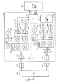
図1は、本発明の実施の形態に係る半導体装置の構成を示すブロック図である。図1に示す半導体装置は、携帯電話機やデータ通信機に実装されるRFIC(Radio−Frequency Integrated Circuit)100と、ベースバンド回路300と、HPA(High Power Amplifier:高出力増幅器)214と、フロントエンドモジュール(FEM:Front End Module)200と、アンテナ210と、受信用Balun(平衡−不平衡変換器)212とを含む。
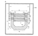
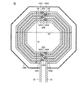
図4は、馬蹄状インダクタ10を示すレイアウト図である。また、図5は、図4におけるA1−A1’線の断面図である。図4および図5を参照して、馬蹄状インダクタ10は、他の回路との接続するための一端部8、他端部9と、金属配線ML1で構成され、直線形状の電流経路P1〜P3を有するインダクタと、キャパシタ11と、複数のコンタクトVIAとを含む。馬蹄状インダクタ10は、いわゆる、LC発振回路と同等な動作を行なう。この馬蹄状インダクタ10には〜約10mA程度の電流が通流する。
本実施の形態の半導体装置と同じ構成であり、その配置が異なる場合を参考例として説明する。たとえば、馬蹄状インダクタ10の電流経路P3と渦巻線状インダクタ20とが最近接になるように配置する。
実施の形態は、図2、図3に示すように、第1の導体層(金属配線ML1)を含んで形成された渦巻線状インダクタ20と、第1の導体層(金属配線ML1)を含んで形成された馬蹄状インダクタ10とを備え、馬蹄状インダクタ10は、開口部が渦巻線状インダクタ20とは反対側に位置するように配置される。
Claims (5)
- 無線を用いて送受信の処理を行なう半導体装置であって、
直交変調器を含む送信部と、
局部発振器を含む受信部とを備え、
前記直交変調器は、第1の導体層を含んで形成された渦巻線状の第1のインダクタを含み、
前記局部発振器は、前記第1の導体層を含んで形成された馬蹄状の第2のインダクタを含み、
前記第2のインダクタは、開口部が前記第1のインダクタとは反対側に位置するように配置される、半導体装置。 - 前記第2のインダクタは、
直線形状の第1〜第3の電流経路を含み、
前記第1の電流経路の一方端と前記第3の電流経路の一方端とによって前記開口部が形成され、
前記第1の電流経路の他方端と前記第2の電流経路の一方端とが接続され、前記第3の電流経路の他方端と前記第2の電流経路の他方端とが接続され、
前記第2のインダクタは、前記第1のインダクタと前記第1〜第3の電流経路の各々との距離のうち、前記第2の電流経路との距離が最小になるような方向に配置される、請求項1に記載の半導体装置。 - 前記第2のインダクタが前記第2の電流経路と垂直方向に平行移動したときに前記第2のインダクタの軌跡が形成される領域に、前記第1のインダクタの少なくとも一部が重なるように前記第1のインダクタが配置される、請求項2に記載の半導体装置。
- 前記第2のインダクタは、線対称であり、
前記線対称の対称軸上に前記第1のインダクタの中心が配置される、請求項3に記載の半導体装置。 - 前記送信部は、
前記第1および第2のインダクタの間に配置されるデジタル回路を含む、請求項1〜4のいずれか1項に記載の半導体装置。
Priority Applications (9)
| Application Number | Priority Date | Filing Date | Title |
|---|---|---|---|
| JP2012099687A JP5912808B2 (ja) | 2012-04-25 | 2012-04-25 | 半導体装置 |
| US13/865,869 US8941213B2 (en) | 2012-04-25 | 2013-04-18 | Semiconductor device |
| CN201310163409.0A CN103378055B (zh) | 2012-04-25 | 2013-04-24 | 半导体器件 |
| CN2013202397685U CN203277374U (zh) | 2012-04-25 | 2013-04-24 | 半导体器件 |
| CN201710324641.6A CN107256854B (zh) | 2012-04-25 | 2013-04-24 | 半导体器件 |
| US14/573,848 US9054936B2 (en) | 2012-04-25 | 2014-12-17 | Semiconductor device having horseshoe and spiral shape inductors |
| US14/724,525 US9319091B2 (en) | 2012-04-25 | 2015-05-28 | Semiconductor device including first inductor of a spiral shape and a second inductor having an opening which is opposite the first inductor |
| US15/068,156 US9461695B2 (en) | 2012-04-25 | 2016-03-11 | Semiconductor device including spiral-shape inductor and horseshoe-shape inductor |
| US15/253,560 US9577698B2 (en) | 2012-04-25 | 2016-08-31 | Semiconductor device including spiral shape inductor and horseshoe shape inductor |
Applications Claiming Priority (1)
| Application Number | Priority Date | Filing Date | Title |
|---|---|---|---|
| JP2012099687A JP5912808B2 (ja) | 2012-04-25 | 2012-04-25 | 半導体装置 |
Publications (3)
| Publication Number | Publication Date |
|---|---|
| JP2013229716A JP2013229716A (ja) | 2013-11-07 |
| JP2013229716A5 JP2013229716A5 (ja) | 2015-04-09 |
| JP5912808B2 true JP5912808B2 (ja) | 2016-04-27 |
Family
ID=49462959
Family Applications (1)
| Application Number | Title | Priority Date | Filing Date |
|---|---|---|---|
| JP2012099687A Active JP5912808B2 (ja) | 2012-04-25 | 2012-04-25 | 半導体装置 |
Country Status (3)
| Country | Link |
|---|---|
| US (5) | US8941213B2 (ja) |
| JP (1) | JP5912808B2 (ja) |
| CN (3) | CN203277374U (ja) |
Families Citing this family (11)
| Publication number | Priority date | Publication date | Assignee | Title |
|---|---|---|---|---|
| JP5912808B2 (ja) * | 2012-04-25 | 2016-04-27 | ルネサスエレクトロニクス株式会社 | 半導体装置 |
| KR102071336B1 (ko) * | 2013-09-30 | 2020-01-30 | 에스케이하이닉스 주식회사 | 반도체 메모리 장치 |
| US9312927B2 (en) * | 2013-11-11 | 2016-04-12 | Qualcomm Incorporated | Tunable guard ring for improved circuit isolation |
| CN105376352B (zh) * | 2014-08-29 | 2019-11-26 | 展讯通信(上海)有限公司 | 移动终端 |
| JP6341852B2 (ja) * | 2014-12-26 | 2018-06-13 | ルネサスエレクトロニクス株式会社 | 半導体装置及びそれを備えた半導体システム |
| JP2017098334A (ja) * | 2015-11-19 | 2017-06-01 | ルネサスエレクトロニクス株式会社 | 半導体装置 |
| US10666302B2 (en) * | 2016-06-21 | 2020-05-26 | Telefonaktiebolaget Lm Ericsson (Publ) | Antenna feed in a wireless communication network node |
| CN106876379B (zh) * | 2016-07-07 | 2019-10-08 | 威盛电子股份有限公司 | 半导体装置 |
| TWI674596B (zh) * | 2018-12-21 | 2019-10-11 | 瑞昱半導體股份有限公司 | 電感裝置及其控制方法 |
| TWI722946B (zh) * | 2019-09-11 | 2021-03-21 | 瑞昱半導體股份有限公司 | 半導體裝置 |
| US11942795B1 (en) | 2022-11-28 | 2024-03-26 | Netronix, Inc. | Multi-antenna system for harvesting energy and transmitting data |
Family Cites Families (8)
| Publication number | Priority date | Publication date | Assignee | Title |
|---|---|---|---|---|
| US6377464B1 (en) * | 1999-01-29 | 2002-04-23 | Conexant Systems, Inc. | Multiple chip module with integrated RF capabilities |
| EP1400012B1 (en) * | 2000-10-10 | 2011-08-31 | California Institute Of Technology | Distributed circular geometry power amplifier architecture |
| JP4192604B2 (ja) | 2003-01-20 | 2008-12-10 | 株式会社村田製作所 | コイル部品 |
| US6825749B1 (en) * | 2004-01-26 | 2004-11-30 | National Applied Research Laboratories National Chip Implementation Center | Symmetric crossover structure of two lines for RF integrated circuits |
| JP2005327931A (ja) | 2004-05-14 | 2005-11-24 | Sony Corp | 集積化インダクタおよびそれを用いた受信回路 |
| JP4541800B2 (ja) * | 2004-08-20 | 2010-09-08 | ルネサスエレクトロニクス株式会社 | インダクタを備えた半導体装置 |
| CN1979704B (zh) * | 2005-12-09 | 2010-06-23 | 胜美达电机(香港)有限公司 | 变压器及其制造方法 |
| JP5912808B2 (ja) * | 2012-04-25 | 2016-04-27 | ルネサスエレクトロニクス株式会社 | 半導体装置 |
-
2012
- 2012-04-25 JP JP2012099687A patent/JP5912808B2/ja active Active
-
2013
- 2013-04-18 US US13/865,869 patent/US8941213B2/en active Active
- 2013-04-24 CN CN2013202397685U patent/CN203277374U/zh not_active Expired - Fee Related
- 2013-04-24 CN CN201710324641.6A patent/CN107256854B/zh active Active
- 2013-04-24 CN CN201310163409.0A patent/CN103378055B/zh active Active
-
2014
- 2014-12-17 US US14/573,848 patent/US9054936B2/en active Active
-
2015
- 2015-05-28 US US14/724,525 patent/US9319091B2/en active Active
-
2016
- 2016-03-11 US US15/068,156 patent/US9461695B2/en active Active
- 2016-08-31 US US15/253,560 patent/US9577698B2/en active Active
Also Published As
| Publication number | Publication date |
|---|---|
| US20150263779A1 (en) | 2015-09-17 |
| US20150103949A1 (en) | 2015-04-16 |
| US9319091B2 (en) | 2016-04-19 |
| CN103378055B (zh) | 2017-09-22 |
| JP2013229716A (ja) | 2013-11-07 |
| US20130285198A1 (en) | 2013-10-31 |
| US9054936B2 (en) | 2015-06-09 |
| CN107256854B (zh) | 2020-05-19 |
| US8941213B2 (en) | 2015-01-27 |
| CN203277374U (zh) | 2013-11-06 |
| CN107256854A (zh) | 2017-10-17 |
| US9461695B2 (en) | 2016-10-04 |
| CN103378055A (zh) | 2013-10-30 |
| US20160197641A1 (en) | 2016-07-07 |
| US9577698B2 (en) | 2017-02-21 |
| US20160373159A1 (en) | 2016-12-22 |
Similar Documents
| Publication | Publication Date | Title |
|---|---|---|
| JP5912808B2 (ja) | 半導体装置 | |
| JP4521602B2 (ja) | マルチモード高周波回路 | |
| US9019168B2 (en) | Frequency stabilization circuit, frequency stabilization device, antenna apparatus and communication terminal equipment, and impedance conversion element | |
| US7199679B2 (en) | Baluns for multiple band operation | |
| JP4709316B2 (ja) | マルチモード高周波回路 | |
| JP2019205007A (ja) | 高周波回路 | |
| JP2013229716A5 (ja) | ||
| US20120194294A1 (en) | Duplexer | |
| JP2014116844A (ja) | 半導体モジュール | |
| JPWO2012105373A1 (ja) | デュプレクサモジュール | |
| KR20210122093A (ko) | 고주파 모듈 및 통신장치 | |
| US20140340261A1 (en) | Dual band antenna | |
| US11757476B2 (en) | Radio frequency module and communication device | |
| WO2022102288A1 (ja) | 高周波モジュール及び通信装置 | |
| US11831292B2 (en) | LC composite component and communication terminal device | |
| WO2022034818A1 (ja) | 高周波モジュール | |
| JPWO2012105375A1 (ja) | フィルタモジュール | |
| US11431361B2 (en) | Radio-frequency module and communication apparatus | |
| WO2022102284A1 (ja) | 高周波モジュール及び通信装置 | |
| US20230103162A1 (en) | High frequency module and communication device | |
| JP2005123728A (ja) | アンテナ共用器およびそれを用いた無線端末 | |
| WO2022160248A1 (zh) | 多频段功率放大电路和射频收发机 | |
| WO2022034819A1 (ja) | 高周波モジュール | |
| JP2006135835A (ja) | 高周波信号処理用電子部品および無線通信システム | |
| US20140340262A1 (en) | Antenna and electronic device including the same |
Legal Events
| Date | Code | Title | Description |
|---|---|---|---|
| A521 | Request for written amendment filed |
Free format text: JAPANESE INTERMEDIATE CODE: A523 Effective date: 20150218 |
|
| A621 | Written request for application examination |
Free format text: JAPANESE INTERMEDIATE CODE: A621 Effective date: 20150218 |
|
| A977 | Report on retrieval |
Free format text: JAPANESE INTERMEDIATE CODE: A971007 Effective date: 20151228 |
|
| A131 | Notification of reasons for refusal |
Free format text: JAPANESE INTERMEDIATE CODE: A131 Effective date: 20160112 |
|
| A521 | Request for written amendment filed |
Free format text: JAPANESE INTERMEDIATE CODE: A523 Effective date: 20160302 |
|
| TRDD | Decision of grant or rejection written | ||
| A01 | Written decision to grant a patent or to grant a registration (utility model) |
Free format text: JAPANESE INTERMEDIATE CODE: A01 Effective date: 20160322 |
|
| A61 | First payment of annual fees (during grant procedure) |
Free format text: JAPANESE INTERMEDIATE CODE: A61 Effective date: 20160401 |
|
| R150 | Certificate of patent or registration of utility model |
Ref document number: 5912808 Country of ref document: JP Free format text: JAPANESE INTERMEDIATE CODE: R150 |